6502.org Forum  Projects  Code  Documents  Tools  Forum
It is currently Sun Apr 28, 2024 8:34 am

All times are UTC


Post new topic Reply to topic  [ 111 posts ]  Go to page Previous  1, 2, 3, 4, 5, 6, 7, 8  Next
Author Message
PostPosted: Fri Aug 11, 2023 4:06 pm 
Offline

Joined: Fri Jul 09, 2021 10:12 pm
Posts: 741
hoglet wrote:
Does it only fail at high clock speeds?

If it fails at 12MHz (say) then you might be able to capture a synchronous trace with the FX2 dev board.

Dave


I haven't tried fx2pipe yet, I think that's what's required for that isn't it? I've also been meaning to ask - I might have a slightly different board to you, does mine really support 48MHz capture? See below:

Code:
gfoot@box:~/logicanalyzer/6502Decoder$ sigrok-cli -d fx2lafw --show
Driver functions:
    Logic analyzer
Scan options:
    conn
fx2lafw:conn=1.41 - Cypress FX2 [S/N: Cypress FX2] with 16 channels: D0 D1 D2 D3 D4 D5 D6 D7 D8 D9 D10 D11 D12 D13 D14 D15
Channel groups:
    Logic: channels D0 D1 D2 D3 D4 D5 D6 D7 D8 D9 D10 D11 D12 D13 D14 D15
Supported configuration options across all channel groups:
    continuous: on, off
    limit_samples: 0 (current)
    conn: 1.41 (current)
    samplerate - supported samplerates:
      20 kHz (current)
      25 kHz
      50 kHz
      100 kHz
      200 kHz
      250 kHz
      500 kHz
      1 MHz
      2 MHz
      3 MHz
      4 MHz
      6 MHz
      8 MHz
      12 MHz
      16 MHz
      24 MHz
      48 MHz
    Supported triggers: 0 1 r f e
    captureratio: 0 (current)


Anyway I added continuous capture and trigger-to-stop behaviour to my bus capture device and got a trace out of it. It's a bit more tricky when the decoder doesn't see the reset, it seems to take it quite a while to get in sync here as I only have data bus and PHI2 signals. I will see what I can do with fx2pipe later on.

It doesn't always report errors - in testing this I had a few runs where the tests passed successfully. But it usually reports an error, and here's an example that I caught a trace of:

Code:
Started testing

regs Y  X  A  PS PCLPCH
01FA 20 C0 02 7C 1F 25
000C FF DF FF 20 FF 02 FF
0200 F0 1C 0F 41 28 20 00 00 00 00
press C to continue or S to skip current test


The trace and lst file are attached - I haven't looked at them in detail yet though, I thought I'd share them straight away as you said you liked analysing this sort of thing! There are a few prediction failures for sure.


Attachments:
decout13.txt.gz [262.92 KiB]
Downloaded 46 times
65C02_extended_opcodes_test.lst.gz [66.24 KiB]
Downloaded 39 times
Top
 Profile  
Reply with quote  
PostPosted: Fri Aug 11, 2023 4:50 pm 
Offline

Joined: Fri Jul 09, 2021 10:12 pm
Posts: 741
Actually judging by the prediction failures there were some issues with the data capture, it looks like it double-counted some samples. I made a script to edit them out, so here's a version of that trace without the bad data samples in it - there are no prediction failures in this one, as I also made it start at a JMP instruction.


Attachments:
filtout13.txt.gz [248.32 KiB]
Downloaded 47 times
Top
 Profile  
Reply with quote  
PostPosted: Fri Aug 11, 2023 5:26 pm 
Offline

Joined: Sun Jun 29, 2014 5:42 am
Posts: 337
gfoot wrote:
I haven't tried fx2pipe yet, I think that's what's required for that isn't it?

Yes, or Dominic B's fx2sharp C# port if you are on windows.
gfoot wrote:
I've also been meaning to ask - I might have a slightly different board to you, does mine really support 48MHz capture?

That's interesting....

I think this is a software difference rather than a hardware one.

The capture process is driven by the firmware that sigrok uploads to the fx2 microcontroller. It seems that in version 1.7 (2019) they added an experimental option for 48MHz capture, with lots of caveats.

I found a blog post about this:
https://www.sigrok.org/blog/sigrok-firm ... 7-released

And here's the relevant commit:
https://github.com/sigrokproject/sigrok ... /b283ba837

I'd be interested how you get on with this.

gfoot wrote:
The trace and lst file are attached - I haven't looked at them in detail yet though, I thought I'd share them straight away as you said you liked analysing this sort of thing! There are a few prediction failures for sure.

I'll have a look now...

Dave


Top
 Profile  
Reply with quote  
PostPosted: Fri Aug 11, 2023 5:44 pm 
Offline

Joined: Sun Jun 29, 2014 5:42 am
Posts: 337
gfoot wrote:
Actually judging by the prediction failures there were some issues with the data capture, it looks like it double-counted some samples. I made a script to edit them out, so here's a version of that trace without the bad data samples in it - there are no prediction failures in this one, as I also made it start at a JMP instruction.

I'm surprised there are no prediction fails if the TSB/TRB Dormann test is hitting a fail.

This sequence just prior to the failure is interesting:
Code:
   32554     7f2a 0 68 ? ? ?
   32555     7f2b 1 29 ? ? ?
   32556     7f2c 2 b0 ? ? ?
   32557     7f2d 3 ff ? ? ?
2516 : 68       : PLA            : 4 : A=FF X=?? Y=20 SP=?? N=1 V=1 D=1 I=1 Z=0 C=1
   32558     7f2e 0 29 ? ? ?
   32559     7f2f 1 02 ? ? ?
2517 : 29 02    : AND #02        : 2 : A=02 X=?? Y=20 SP=?? N=0 V=1 D=1 I=1 Z=0 C=1
   32560     7f30 0 c5 ? ? ?
   32561     7f31 1 0e ? ? ?
   32562     7f32 2 ff ? ? ?
2519 : C5 0E    : CMP 0E         : 3 : A=02 X=?? Y=20 SP=?? N=0 V=1 D=1 I=1 Z=0 C=0

This is testing the Z flag (on the stack) against the expected value. After the AND instruction, A can only be 0 or 2, yet the CMP against the expected value is reading FF from address 0E. That's clearly wrong, and if memory modelling was enabled I would expect an error to be flagged, because the previous CMP 0E read a value of 02:
Code:
   32496     7ef0 0 c5 ? ? ?
   32497     7ef1 1 0e ? ? ?
   32498     7ef2 2 02 ? ? ?
24E9 : C5 0E    : CMP 0E         : 3 : A=02 X=?? Y=20 SP=?? N=0 V=0 D=0 I=0 Z=1 C=1

What options are you running decode6502 with?

Memory modelling is disabled by default, and needs --mem=00f to enable it.

I suspect the failure here is stray memory writes.

Dave


Top
 Profile  
Reply with quote  
PostPosted: Fri Aug 11, 2023 6:45 pm 
Offline

Joined: Fri Jul 09, 2021 10:12 pm
Posts: 741
Ah yes, well spotted - I thought I had memory modelling enabled, but I had left it out. There are two memory modeling failures in the trace - the one you spotted, and one which is due to the address in question being a 6522 register.

Given that the error report listed 0E as containing FF as well, it does look like a faulty write occurred at some point, rather than this being a faulty read.

I wonder whether tsb/trb could somehow cause this - as I ran a long stress test in the past without any similar errors. I believe when it's failed in the Dormann tests it's also always been in this specific test.

Edit: Here's the trace with memory logging and checking enabled:

Code:
   32496     7ef0 0 c5 ? ? ?
   32497     7ef1 1 0e ? ? ?
   32498     7ef2 2 02 ? ? ?
Rd:   24E9 = C5
Rd:   24EA = 0E
Rd:   000E = 02
24E9 : C5 0E    : CMP 0E         : 3 : A=02 X=?? Y=20 SP=?? N=0 V=0 D=0 I=0 Z=1 C=1
   32499     7ef3 0 f0 ? ? ?
   32500     7ef4 1 03 ? ? ?
   32501     7ef5 2 20 ? ? ?
Rd:   24EB = F0
Rd:   24EC = 03
24EB : F0 03    : BEQ 24F0       : 3 : A=02 X=?? Y=20 SP=?? N=0 V=0 D=0 I=0 Z=1 C=1
   32502     7ef6 0 a5 ? ? ?
   32503     7ef7 1 0f ? ? ?
   32504     7ef8 2 20 ? ? ?
Rd:   24F0 = A5
Rd:   24F1 = 0F
Rd:   000F = 20
24F0 : A5 0F    : LDA 0F         : 3 : A=20 X=?? Y=20 SP=?? N=0 V=0 D=0 I=0 Z=0 C=1
   32505     7ef9 0 c5 ? ? ?
   32506     7efa 1 0c ? ? ?
   32507     7efb 2 20 ? ? ?
Rd:   24F2 = C5
Rd:   24F3 = 0C
Rd:   000C = 20
24F2 : C5 0C    : CMP 0C         : 3 : A=20 X=?? Y=20 SP=?? N=0 V=0 D=0 I=0 Z=1 C=1
   32508     7efc 0 f0 ? ? ?
   32509     7efd 1 03 ? ? ?
   32510     7efe 2 20 ? ? ?
Rd:   24F4 = F0
Rd:   24F5 = 03
24F4 : F0 03    : BEQ 24F9       : 3 : A=20 X=?? Y=20 SP=?? N=0 V=0 D=0 I=0 Z=1 C=1
   32511     7eff 0 84 ? ? ?
   32512     7f00 1 0c ? ? ?
   32513     7f01 2 20 ? ? ?
Rd:   24F9 = 84
Rd:   24FA = 0C
Wr:   000C = 20
24F9 : 84 0C    : STY 0C         : 3 : A=20 X=?? Y=20 SP=?? N=0 V=0 D=0 I=0 Z=1 C=1
   32514     7f02 0 a9 ? ? ?
   32515     7f03 1 ff ? ? ?
Rd:   24FB = A9
Rd:   24FC = FF
24FB : A9 FF    : LDA #FF        : 2 : A=FF X=?? Y=20 SP=?? N=1 V=0 D=0 I=0 Z=0 C=1
   32516     7f04 0 48 ? ? ?
   32517     7f05 1 a5 ? ? ?
   32518     7f06 2 ff ? ? ?
Rd:   24FD = 48
24FD : 48       : PHA            : 3 : A=FF X=?? Y=20 SP=?? N=1 V=0 D=0 I=0 Z=0 C=1
   32519     7f07 0 a5 ? ? ?
   32520     7f08 1 0d ? ? ?
   32521     7f09 2 df ? ? ?
Rd:   24FE = A5
Rd:   24FF = 0D
Rd:   000D = DF
24FE : A5 0D    : LDA 0D         : 3 : A=DF X=?? Y=20 SP=?? N=1 V=0 D=0 I=0 Z=0 C=1
   32522     7f0a 0 28 ? ? ?
   32523     7f0b 1 04 ? ? ?
   32524     7f0c 2 b0 ? ? ?
   32525     7f0d 3 ff ? ? ?
Rd:   2500 = 28
2500 : 28       : PLP            : 4 : A=DF X=?? Y=20 SP=?? N=1 V=1 D=1 I=1 Z=1 C=1
   32526     7f0e 0 04 ? ? ?
   32527     7f0f 1 0c ? ? ?
   32528     7f10 2 20 ? ? ?
   32529     7f11 3 20 ? ? ?
   32530     7f12 4 ff ? ? ?
Rd:   2501 = 04
Rd:   2502 = 0C
Rd:   000C = 20
Wr:   000C = FF
2501 : 04 0C    : TSB 0C         : 5 : A=DF X=?? Y=20 SP=?? N=1 V=1 D=1 I=1 Z=1 C=1
   32531     7f13 0 08 ? ? ?
   32532     7f14 1 c5 ? ? ?
   32533     7f15 2 ff ? ? ?
Rd:   2503 = 08
2503 : 08       : PHP            : 3 : A=DF X=?? Y=20 SP=?? N=1 V=1 D=1 I=1 Z=1 C=1
   32534     7f16 0 c5 ? ? ?
   32535     7f17 1 0d ? ? ?
   32536     7f18 2 df ? ? ?
Rd:   2504 = C5
Rd:   2505 = 0D
Rd:   000D = DF
2504 : C5 0D    : CMP 0D         : 3 : A=DF X=?? Y=20 SP=?? N=0 V=1 D=1 I=1 Z=1 C=1
   32537     7f19 0 f0 ? ? ?
   32538     7f1a 1 03 ? ? ?
   32539     7f1b 2 20 ? ? ?
Rd:   2506 = F0
Rd:   2507 = 03
2506 : F0 03    : BEQ 250B       : 3 : A=DF X=?? Y=20 SP=?? N=0 V=1 D=1 I=1 Z=1 C=1
   32540     7f1c 0 68 ? ? ?
   32541     7f1d 1 48 ? ? ?
   32542     7f1e 2 b0 ? ? ?
   32543     7f1f 3 ff ? ? ?
Rd:   250B = 68
250B : 68       : PLA            : 4 : A=FF X=?? Y=20 SP=?? N=1 V=1 D=1 I=1 Z=0 C=1
   32544     7f20 0 48 ? ? ?
   32545     7f21 1 09 ? ? ?
   32546     7f22 2 ff ? ? ?
Rd:   250C = 48
250C : 48       : PHA            : 3 : A=FF X=?? Y=20 SP=?? N=1 V=1 D=1 I=1 Z=0 C=1
   32547     7f23 0 09 ? ? ?
   32548     7f24 1 02 ? ? ?
Rd:   250D = 09
Rd:   250E = 02
250D : 09 02    : ORA #02        : 2 : A=FF X=?? Y=20 SP=?? N=1 V=1 D=1 I=1 Z=0 C=1
   32549     7f25 0 c9 ? ? ?
   32550     7f26 1 ff ? ? ?
Rd:   250F = C9
Rd:   2510 = FF
250F : C9 FF    : CMP #FF        : 2 : A=FF X=?? Y=20 SP=?? N=0 V=1 D=1 I=1 Z=1 C=1
   32551     7f27 0 f0 ? ? ?
   32552     7f28 1 03 ? ? ?
   32553     7f29 2 20 ? ? ?
Rd:   2511 = F0
Rd:   2512 = 03
2511 : F0 03    : BEQ 2516       : 3 : A=FF X=?? Y=20 SP=?? N=0 V=1 D=1 I=1 Z=1 C=1
   32554     7f2a 0 68 ? ? ?
   32555     7f2b 1 29 ? ? ?
   32556     7f2c 2 b0 ? ? ?
   32557     7f2d 3 ff ? ? ?
Rd:   2516 = 68
2516 : 68       : PLA            : 4 : A=FF X=?? Y=20 SP=?? N=1 V=1 D=1 I=1 Z=0 C=1
   32558     7f2e 0 29 ? ? ?
   32559     7f2f 1 02 ? ? ?
Rd:   2517 = 29
Rd:   2518 = 02
2517 : 29 02    : AND #02        : 2 : A=02 X=?? Y=20 SP=?? N=0 V=1 D=1 I=1 Z=0 C=1
   32560     7f30 0 c5 ? ? ?
   32561     7f31 1 0e ? ? ?
   32562     7f32 2 ff ? ? ?
Rd:   2519 = C5
Rd:   251A = 0E
Rd:   000E = FF
memory modelling failed at   000E: expected 02 actual FF
2519 : C5 0E    : CMP 0E         : 3 : A=02 X=?? Y=20 SP=?? N=0 V=1 D=1 I=1 Z=0 C=0 prediction failed

It does look like it's the TSB instruction that could be causing the fault - writing FF to 0C but perhaps that's causing my circuit to write it to 0E as well. I'm not sure why this would only affect TSB but will check and rerun my memory stress test and see if that's also failing now.

Edit 2 - some memory accesses don't seem to appear in the trace. This was with --mem=FFF. Stack operations in particular seem to not get listed, nor idle bus cycles.


Top
 Profile  
Reply with quote  
PostPosted: Fri Aug 11, 2023 9:26 pm 
Offline

Joined: Sun Jun 29, 2014 5:42 am
Posts: 337
gfoot wrote:
Ah yes, well spotted - I thought I had memory modelling enabled, but I had left it out. It does look like it's the TSB instruction that could be causing the fault - writing FF to 0C but perhaps that's causing my circuit to write it to 0E as well. I'm not sure why this would only affect TSB but will check and rerun my memory stress test and see if that's also failing now.

The most likely source of stray writes is the addess bus changing during the write cycle (i.e. when RAM nWE is low). This might be happening at either end of the write cycle.

If you slow the clock down and the problem goes away, then I think that's an indication that the problem is at the start of the write cycle.

This is running at 25.175MHz with a 35% positive duty cycle?
gfoot wrote:
Edit 2 - some memory accesses don't seem to appear in the trace. This was with --mem=FFF. Stack operations in particular seem to not get listed, nor idle bus cycles.

That's because the stack pointer is unknown, because the trace doesn't include a TXS.

If you force an initial stack pointer value (e.g. --sp=ff) then stack accesses should show up as well.

Dave


Top
 Profile  
Reply with quote  
PostPosted: Fri Aug 11, 2023 11:45 pm 
Offline

Joined: Fri Jul 09, 2021 10:12 pm
Posts: 741
hoglet wrote:
The most likely source of stray writes is the addess bus changing during the write cycle (i.e. when RAM nWE is low). This might be happening at either end of the write cycle.

If you slow the clock down and the problem goes away, then I think that's an indication that the problem is at the start of the write cycle.

This is running at 25.175MHz with a 35% positive duty cycle?

No this is 25.175MHz from a crystal oscillator, the signal is a pretty good square wave with some overshoot, and close to 50% duty cycle. Slowing the clock is unfortunately not as trivial as I'd like it to be! 16MHz is about the minimum at the moment, but it's not clear whether that actually improved things.

I'm still interested in the reason for the failure, and why it affected the Dormann code but not my own tests, so I tried quite a bit to reproduce the failure in my own code. General RAM write/read soak tests don't seem to fail, covering the whole address space, including the specific addresses used in the Dormann test, so I made one that was closer to what it was doing and gradually made my test closer and closer to the exact scenario in the Dormann test.

The following code didn't fail, even running for several minutes at about 80 million passes per second:

Code:
    lda #$ff : sta $c
    lda #$02 : sta $e
    lda #$ff

    tsb $c

    ldx $e
    cpx #2
    bne fail

However, if I make it match one of the Dormann fail cases more closely - storing $20 at $c and loading A with $df instead of $ff - then it fails almost immediately.

As you said, it seemed likely that the address lines were changing during the RAM write. I had a hunch this was due to the RAM's /WE signal being held just a bit too long, and there was a simple change I colud make to shift that write window slightly earlier - it was being driven by a 74AHCT139 whose /E input was connected directly to PHI2, and PHI2 comes from an OR gate used to stretch the clock sometimes. Connecting the 74AHCT139's /E pin to the unstretched clock instead of PHI2 causes it to arrive slightly earlier, and then this test runs perfectly for long periods.

So I wondered whether it was due to the CPU starting to push the next program counter to the address bus before the RAM's write had been shut off - however it doesn't seem to depend upon exactly what the next program counter value is. I tried offsetting things for example so that the next instruction's address ended with $c - so there'd be no change to the low address lines between cycles - and the test still failed immediately. So in fact it doesn't seem to depend upon what the address of the next instruction is - it must just be general fluctuations in the address bus early in phase 1.

It is also very curious that this specific set of operands - not even just the order of instructions - causes the problem, and I suspect it will still fail sometimes, as this wasn't a very scientific solution, so broader stress tests are probably needed.


Top
 Profile  
Reply with quote  
PostPosted: Sat Aug 12, 2023 6:31 am 
Offline

Joined: Sun Jun 29, 2014 5:42 am
Posts: 337
gfoot wrote:
I'm still interested in the reason for the failure, and why it affected the Dormann code but not my own tests, so I tried quite a bit to reproduce the failure in my own code.

If you want to delve further, I would setup the failing test case to run continuously, then trigger a scope off the rising edge of RAM nWE and use the other channel to probe each address line in turn. Pay particular attention to A1.
gfoot wrote:
So I wondered whether it was due to the CPU starting to push the next program counter to the address bus before the RAM's write had been shut off - however it doesn't seem to depend upon exactly what the next program counter value is. I tried offsetting things for example so that the next instruction's address ended with $c - so there'd be no change to the low address lines between cycles - and the test still failed immediately. So in fact it doesn't seem to depend upon what the address of the next instruction is - it must just be general fluctuations in the address bus early in phase 1.

With this test, I would expect the lower nibble of the address bus to be stable at $0c. I don't see how other address lines changing early can corrupt $0e. This is pretty convincing evidence that some else is going on.
gfoot wrote:
However, if I make it match one of the Dormann fail cases more closely - storing $20 at $c and loading A with $df instead of $ff - then it fails almost immediately.

In my experience these kind of RAM write problems can be very fickle. In this case you are changing the number of bits TSB sets from one to seven. It is possible this is causing crosstalk onto A1, smearing the write of $ff onto both addresses $c and $e. This failure mode would be insensitive to the address of the next instruction.

With a small test case like this and a decent scope you should be able to see what's actually happening. Which model Hantek scope do you have?

Dave


Top
 Profile  
Reply with quote  
PostPosted: Sat Aug 12, 2023 1:53 pm 
Offline

Joined: Fri Jul 09, 2021 10:12 pm
Posts: 741
hoglet wrote:
If you want to delve further, I would setup the failing test case to run continuously, then trigger a scope off the rising edge of RAM nWE and use the other channel to probe each address line in turn. Pay particular attention to A1.

I can't really probe that effectively because it's one of those cases where applying the scope probe there makes the problem go away. Inserting a wire and touching it also prevents the issue - so I think it's likely a signal quality problem due to the breadboard circuit's construction. Probing VCC near the RAM chip shows a fair amount of general noise (which I've come to expect with these circuits on breadboards) and especially a noticeable drop in VCC near the RAM chip during write operations - briefly down to a little under 4V - and adding a decoupling capacitor there also prevents the problem.

That is a proper general solution to the problem, and this should all be better on the PCB if I ever get around to sending that off! I will shore up the decoupling on the prototype circuit as well though, as while I hadn't intended to keep using it, it has worked better than I expected and it's been quite nice to work on and expand.

Regarding the specific code and data that caused the failure, as it might become important again at higher clock frequencies, I haven't tested other address lines thoroughly, but I did try swapping A0 and A1 over. A0 was connected to pin 1 of the 32K SRAM chip - its A14 - and A1 was connected to pin 2, A12. Swapping them over prevented the error, though the VCC drop was still present, and changing the code to watch $d instead of $e made it occur again. So it seems that when the VCC drop occurs, the SRAM chip's response varies across its address pins.

My theory was that the data bus transition from $20 to $ff was causing the CPU, perhaps, to briefly draw more power as it drives the bus to the new level. So with that theory, I also looked in a bit more depth at other instructions. I tried read-modify-write instructions like "inc" and "dec", and simply storing with "sta", but couldn't get the error to occur with those. Even "dec $c" with $c initialised to zero didn't cause the issue - despite having a similar swing of the data bus from lots of clear bits to lots of set bits between cycles, and a brief spike down in VCC similar to the one I had before.

Code:
loop:
    lda #$00 : sta $c
    lda #$02 : sta $e
    lda #$df

    dec $c

    ldx $e
    cpx #$02
    bne fail

    inc 0 : bne loop
    inc 1 : bne loop
    (...)


So I'm still left with "tsb" being the only instruction that actually causes the error. Perhaps it is due to the unusual way it sets the flags based on one operation, but then performs a store based on another - however, it's all done on different bus cycles, and I don't see anything unusual about the timing of the write operation on the scope. During write operations I see the data bus being rather slow at rising up, but that's not unique to this instruction.

I think I'm going to park that investigation and move on with other things, given the immediate issue is solved, and just bear in mind that "tsb" might be a more fragile instruction than the others for future reference.

Quote:
With a small test case like this and a decent scope you should be able to see what's actually happening. Which model Hantek scope do you have?

It's DSO4254C - it has up to four channels, with sampling rates from 250M/s to 1G/s depending how many channels are active. I've found it OK for this sort of frequency around the VGA speed, but the front end is a bit quirky and sometimes does annoying things like rendering smoothed-out waveforms instead of the actual data that was sampled!


Top
 Profile  
Reply with quote  
PostPosted: Wed Aug 16, 2023 6:55 pm 
Offline

Joined: Fri Jul 09, 2021 10:12 pm
Posts: 741
As the breadboard prototype has been working well, I updated my PCB layouts to match it and sent them off for manufacture. The main change from the initial breadboard prototype was moving from use of RDY to clock stretching, by adding a quad-OR IC so that PHI2 could be held high when RDY would have been low in the old design. The PCBs also have a footprint for the DS1086Z programmable oscillator that was recommended earlier in this thread, so I'll more easily be able to test at different clock speeds.

As it takes a while to make and ship the PCBs, in the meantime I've been thinking about future enhancements to make. This post is mostly going to be briefly mentioning some of the ideas I've had so apologies if it's a bit disjointed - these are early thoughts.

What I've already designed should run quickly and be quite expandable. Potentially some sort of VGA board could plug into one of the I/O slots. The I/O slots don't have many address lines, so it would need to have a command-based register interface rather than memory mapped framebuffer. It would be pretty easy though to make such an interface to one of my existing VGA circuits, I think, and I've been meaning to do that for a while so that I can then expand on it to produce something that's a bit more GPU-like - hardware accelerated drawing operations for example.

Back on the CPU module, I used discrete logic ICs for clock stretching and high level address decoding, because the propagation delays with AHCT parts seemed lower than the nominal delay of the simple PLDs I'm using:
Attachment:
File comment: Original design, discrete glue logic
fastpdip6502_cpumodule_glue_discrete.png
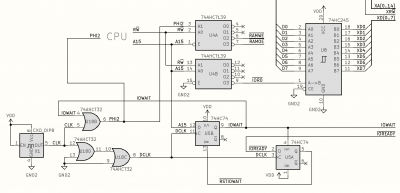
fastpdip6502_cpumodule_glue_discrete.png [ 39.08 KiB | Viewed 28616 times ]


However, in practice the PLDs seem to perform much better than the datasheet would imply, and I'd like to swap out the 74AHCT139, 74AHCT74, and 74ACHT32 for an ATF16V8. That can easily do the same job, should be faster, and will have spare pins for other things:

Attachment:
File comment: Potential PLD-based glue logic design
fastpdip6502_cpumodule_glue_pld1.png
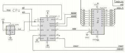
fastpdip6502_cpumodule_glue_pld1.png [ 25.5 KiB | Viewed 28616 times ]


Potentially I could make this update to the PCB design and fab that as a variant of the CPU module, as it is swappable.

It might also be interesting to make a 4-layer board version of the CPU module and see whether that's able to run any faster than the 2-layer board - again this can just be plugged into the existing I/O module without requiring changes there.

For general system improvement, I'm interested in revisiting the memory map and RAM/ROM split. Currently there's 32K of RAM from $0000-$7FFF, with 32K of ROM from $8000-$FFFF except for the region from $FF00-$FFBF which is decoded for I/O (VIAs, etc). A big disadvantage of this memory map is that in this system any code that runs from ROM is rather slow, as all ROM accesses are cycle-stretched just like I/O is. The plan was to just copy the code to RAM and run it there, especially if it's code that benefits from speed, but it means that half the address space is then lost, and there's only 32K of usable memory. It's OK for a prototype but not so good for general purpose use.

The reason for this memory map, initially, was to minimize the address decoding overhead for the RAM, to allow it to run as quickly as possible. Having one IC always selected achieves that, with initialy address decoding based only on A15 - if A15 is 0, it's a RAM access, otherwise it's either ROM or I/O and needs clock-stretching either way. I'm not able to find the 64MB ICs that Michael uses - 32MB is the only one I find in stock at the usual places, at this speed (~12ns). However I can of course use two of them, with one selected by A15 being low and the other selected by A14 being low and A15 being high, for example. In fact with the glue logic replaced with the PLD, there's enough spare pins to wire through all the address bits from 15 down to 9, and have the PLD decide whether high address space accesses are RAM or I/O/ROM.

Attachment:
File comment: PLD-based design with 64KB RAM
fastpdip6502_cpumodule_glue_pld2.png
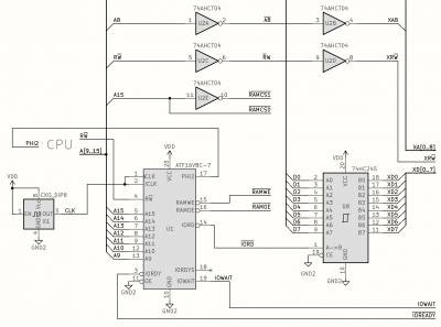
fastpdip6502_cpumodule_glue_pld2.png [ 39.76 KiB | Viewed 28616 times ]


In this case, the PLD would disable RAMOE and RAMWE during I/O access, and the inverters drive the two RAM CS signals regardless of I/O decoding. The other inverters are also acting to buffer A8 and RWB for passing off the board, so I can get rid of the existing transceiver for the high address lines. I could use an ATF 22V10 PLD instead of 16V8, to get more pins and do the inverting in the PLD, but I found in the past that the 22V10s use a lot more current and run a lot warmer, and I didn't like that, so I try to fit things into 16V8s instead now.

This would lead to a memory map with one bank of RAM from $0000-$7FFF, another from $8000-$FDFF, then ROM from $FE00-$FFFF minus the same I/O window as before from $FF00-$FFBF. That is not much ROM but I believe it is enough for an SD card bootloader or something similar. This should be possible to do with changes to the CPU module alone - a new PCB could be fabricated that would plug into the existing I/O module.

I seem to have a spare inverter as well, which could actually be used to still pass A9 to the I/O board in addition to A0-8, allowing twice as much ROM if that turns out to be needed/useful.

A nice side-effect of this would be that the CPU module no longer needs to send so many address lines to the I/O module. As noted above it saves a transceiver, and also the connector I have between the two is rather overloaded at the moment - it's a 36-pin card edge connection, with 29 data signals and only 7 power/ground lines. Getting rid of 6 address lines will bring it to 23 data signals and 13 power/ground return lines, which is not ideal, but is a better balance.

Attachment:
File comment: CPU module card edge connector
cpumodule_connector.png
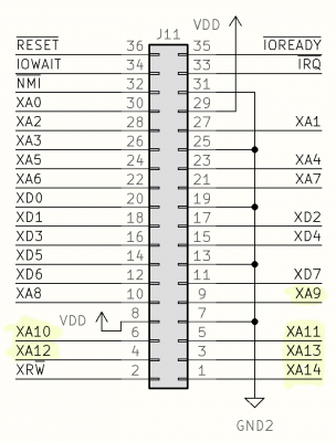
cpumodule_connector.png [ 27.89 KiB | Viewed 28616 times ]


Another interesting option is to go ROMless, and preload the RAM - this is why I've been asking about those techniques on other threads, especially regarding SPI EEPROMs. Dr Jeffyl's scheme is very interesting as a hack; or copy data to RAM from a parallel or serial ROM can be done with just a few ICs; or from a microcontroller, maybe even the FX2LP logic analyser with some patched firmware. This would free up three more address lines that would no longer need to go to the I/O module.

For a more retro feel I have also thought a bit about DMAing data from floppy disk into RAM to boot from. The floppy disk driver circuit that I built last year could do this fairly easily if I stored the boot code in the last 256-byte sector of every track on the disk, and rigged the DMA system to fill from $FF00-$FFFF - I wouldn't need to care which track the drive was on, nor decode sector headers, just read every sector into memory and after a couple of index holes to ensure the disk is up to speed, stop and release the CPU to run whatever was loaded last. Again this could be done entirely within the CPU module I believe - though it may be more sensible to redesign the I/O module to properly support DMA.

Anyway I think those are all my thoughts at the moment - quite a mixed bag I'm sure! Mostly right now I'm looking forward to the PCBs arriving in a few days, and being able to test this design more completely.


Top
 Profile  
Reply with quote  
PostPosted: Thu Aug 17, 2023 7:05 am 
Offline
User avatar

Joined: Wed Feb 13, 2013 1:38 pm
Posts: 586
Location: Michigan, USA
gfoot wrote:
I'm not able to find the 64MB ICs that Michael uses ...
That's the only part I use that I haven't found available at distributors, so far. I purchase 'skinny' 64KB 10, 15, or 20-nS parts at bargain prices (~68¢ each) from this vendor listing on AliExpress. Shipping takes approximately 20 days from date of order (09-Jul-23 to 29-Jul-23 on my last order).

Good luck on your project...


Top
 Profile  
Reply with quote  
PostPosted: Thu Aug 17, 2023 8:42 am 
Offline

Joined: Fri Jul 09, 2021 10:12 pm
Posts: 741
Michael wrote:
That's the only part I use that I haven't found available at distributors, so far. I purchase 'skinny' 64KB 10, 15, or 20-nS parts at bargain prices (~68¢ each) from this vendor listing on AliExpress. Shipping takes approximately 20 days from date of order (09-Jul-23 to 29-Jul-23 on my last order).

Good luck on your project...

Thanks! I'll get some ordered.


Top
 Profile  
Reply with quote  
PostPosted: Thu Aug 17, 2023 2:16 pm 
Offline

Joined: Fri Mar 18, 2022 6:33 pm
Posts: 432
Your overall concept for this project seems a lot like what I'm going for with Blue August. I'm wondering about this:

gfoot wrote:
The reason for this memory map, initially, was to minimize the address decoding overhead for the RAM, to allow it to run as quickly as possible. Having one IC always selected achieves that, with initialy address decoding based only on A15 - if A15 is 0, it's a RAM access, otherwise it's either ROM or I/O and needs clock-stretching either way.
This is elegant; but does that mean *all* I/O transactions are slow, including VIA access? I have it so that the VIA is clocked at the same frequency as the RAM and the CPU only slows down for ROM and slow I/O (like my old ACIA). It seems like you're doing the inverse of that - the constant system clock is the slow clock, and the CPU only speeds up to access the RAM. Rather than clock stretching, it's clock shrinking! I hadn't thought of doing it that way, but it does seem like it could simplify some things.

_________________
"The key is not to let the hardware sense any fear." - Radical Brad


Top
 Profile  
Reply with quote  
PostPosted: Thu Aug 17, 2023 4:31 pm 
Offline

Joined: Fri Jul 09, 2021 10:12 pm
Posts: 741
Paganini wrote:
gfoot wrote:
The reason for this memory map, initially, was to minimize the address decoding overhead for the RAM, to allow it to run as quickly as possible. Having one IC always selected achieves that, with initialy address decoding based only on A15 - if A15 is 0, it's a RAM access, otherwise it's either ROM or I/O and needs clock-stretching either way.
This is elegant; but does that mean *all* I/O transactions are slow, including VIA access?

Yes, all I/O transactions set the IOWAIT signal and the IOREADY signal won't be sampled until the next clock cycle, so the soonest time such an operation could finish is on the next rising edge of the original clock. But the current I/O module design always stretches the clock to cover the next two cycles of its own clock, and then a random bit more due to the clocks not being synchronised. I was quite conservative here and didn't really care how slow ROM and I/O operations became, for this first pass. In practice with a 25.175MHz CPU clock and 16MHz I/O clock I think this ended up averaging something like 6MHz-9MHz overall cycle rate when running from ROM.

Quote:
I have it so that the VIA is clocked at the same frequency as the RAM and the CPU only slows down for ROM and slow I/O (like my old ACIA). It seems like you're doing the inverse of that - the constant system clock is the slow clock, and the CPU only speeds up to access the RAM. Rather than clock stretching, it's clock shrinking! I hadn't thought of doing it that way, but it does seem like it could simplify some things.

I guess you could view it that way - but really it is the CPU's clock signal that's being stretched - it's actually just forced high during I/O operations, so the duty cycle gets really extended.

Plasmo mentioned that he thinks he's had a 6502+RAM+6522 combination running at about 25MHz in the past, so I think it's probably possible to have the 6522 on the fast bus in general and still get good speeds - however, even if the 6522 is capable of keeping up, simply having it on the bus presents additional loads, both from its pins and also the PCB traces to reach them, and also means that the relevant address decoding moves back on to the critical path. I don't know how much these things matter in practice, but at least for a first pass I wanted to focus my design on ensuring the 6502+RAM could run at their best possible rate, without letting other things compromise that.


Top
 Profile  
Reply with quote  
PostPosted: Fri Aug 18, 2023 3:44 pm 
Offline

Joined: Fri Jul 09, 2021 10:12 pm
Posts: 741
The PCBs arrived today - I have a VIA expansion board on the left, the I/O board in the middle, and a CPU board on the right:

Attachment:
20230818_160825.jpg
20230818_160825.jpg [ 1.29 MiB | Viewed 28496 times ]

Attachment:
20230818_160854.jpg
20230818_160854.jpg [ 1.63 MiB | Viewed 28496 times ]


I wasn't sure what to expect from the card edge connections, but they came out well. Crucially, they do fit into the sockets! I'm aware that the tin will get scratched off and connection quality will suffer, but interested to see how much abuse they take before that happens. I asked for a chamfered edge on the cpu board but not the VIA board, to see what the difference was like. I don't think it matters much.

The card edge sockets require a fairly thick board, these are 1.6mm.

I also made some adaptor boards to use the SMD programmable oscillator (DS1086Z) in the socket for a PDIP-8 oscillator, and break out the programing pins:

Attachment:
20230818_152442.jpg
20230818_152442.jpg [ 967.64 KiB | Viewed 28496 times ]


Top
 Profile  
Reply with quote  
Display posts from previous:  Sort by  
Post new topic Reply to topic  [ 111 posts ]  Go to page Previous  1, 2, 3, 4, 5, 6, 7, 8  Next

All times are UTC


Who is online

Users browsing this forum: No registered users and 26 guests


You cannot post new topics in this forum
You cannot reply to topics in this forum
You cannot edit your posts in this forum
You cannot delete your posts in this forum
You cannot post attachments in this forum

Search for:
Jump to: