6502.org Forum  Projects  Code  Documents  Tools  Forum
It is currently Sat Apr 27, 2024 8:15 pm

All times are UTC


Post new topic Reply to topic  [ 111 posts ]  Go to page Previous  1, 2, 3, 4, 5, 6 ... 8  Next
Author Message
PostPosted: Fri Jul 21, 2023 12:10 am 
Offline

Joined: Fri Jul 09, 2021 10:12 pm
Posts: 741
I think there were plenty of mistakes in my logic earlier - hopefully this is a bit better now! This is using discrete D-flipflops rather than a PLD, though I may still go either way on that. The main change here is making use of asynchronous resets to reduce some of the complexity and deal better with the end of an I/O cycle - I'm pretty sure that's OK now, and this diagram shows two I/O cycles in quick succession as well as an I/O cycle without another following it.

Attachment:
iomodule_wait_timing_dffs.png
iomodule_wait_timing_dffs.png [ 31.54 KiB | Viewed 28705 times ]


IOCLK is probably 4MHz, we have two flipflops in a row before IOCS is generated so hopefully decent metastability safeguards, one more flipflop to generate the IOREADY signal, and no extra glue logic needed so the only propagation delays are in the flipflops which are all clocked by IOCLK.

The delay between IOREADY rising and IOWAIT falling is probably about 30ns plus the clock period of the CPU clock, so to arrive in time for the next IOCLK it could probably support clock periods up to about 200ns, i.e. frequencies down to about 5MHz. So long as the CPU clock is always faster than that, IOWAIT will get reset in time to avoid wrongly repeating an I/O cycle.

I did think about more robust ways to make that safe, and it's mostly down to the way the IOWAIT/IOREADY handshake works between the two modules. If the I/O module responded straight away to IOWAIT then the system module could deassert it, and still wait for IOREADY, acknowledging that separately. Then either module could wait for the other as necessary. I think it's probably OK how it is though.

It's getting to a point where I can probably soon finish designing a basic I/O module, and post a whole-system schematic.


Top
 Profile  
Reply with quote  
PostPosted: Wed Aug 02, 2023 4:15 am 
Offline

Joined: Fri Jul 09, 2021 10:12 pm
Posts: 741
I fleshed out the design more in KiCad, and did a few PCB layouts. It's suffered quite a lot of feature-creep - it was meant to be a minimal test, but since I added in the whole I/O module, I couldn't help but make that a bit more fully-featured too. Oh well! I have an aversion to making PCBs without cramming as much as I can think of in - the idea is to make sure at least something doesn't work, as otherwise I'll just regret not being more ambitious with what I put on the PCB the first time around. We'll see, anyway.

Before sending PCBs off to manufacture, I also wanted to test the basic design on a breadboard. To do that I cloned the KiCad project and cut the complexity back a lot, including dropping the address bus to just eight bits, as that saves some ICs and a lot of wires, and is still enough to run some basic tests and probe the circuit to check the wait states are working as designed. This is the cut back schematic for the breadboard prototype:

Attachment:
File comment: CPU module
schematic-cpumodule.png
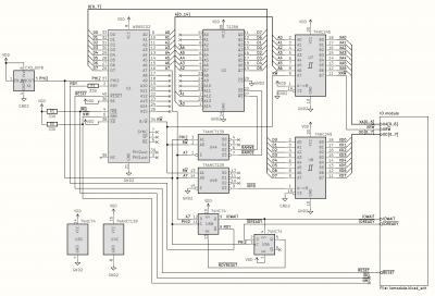
schematic-cpumodule.png [ 85.65 KiB | Viewed 28625 times ]

Attachment:
File comment: I/O+ROM module
schematic-iomodule.png
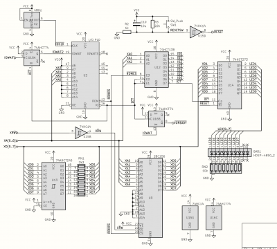
schematic-iomodule.png [ 85.59 KiB | Viewed 28625 times ]


The 8-bit address space is divided into RAM ($00-$7F), ROM ($80-$EF), I/O ($F0-$F7), and ROM again ($F8-$FF). This is just a contraction of the 16-bit address space in the main design - the PLD code is the same for both, I just wired different address lines through to it. In the 16-bit version the ROM-to-I/O cut-off is at $FF00 and the upper I/O-to-ROM boundary is at $FFC0.

I used KiCad's PCB tool to design a sensible breadboard layout, then built it up this evening - here's the result:

Attachment:
File comment: Breadboard prototype
breadboard.jpg
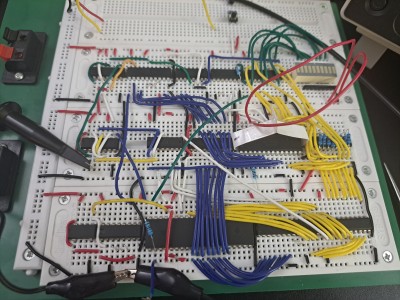
breadboard.jpg [ 4 MiB | Viewed 28625 times ]


The CPU module is mostly on the bottom row, with the I/O and ROM further back. It's using a 16MHz oscillator, with a counter to divide it by up to 16. The counter is also used to generate the slower clock for the I/O module, which consequently is currently synchronous with the CPU clock - that's not the intended long term design though.

The ROM contains a couple of test programs that use the LEDs in the corner to communicate their results. One just counts up on the LEDs, the other performs RAM operations and verifies the results. I can extend this test suite fairly easily, subject to the caveat that I only have a 256-byte address space and less than half of that is ROM - still I think it's enough to make some useful test programs, and when the PCBs are done the address space limitation will be gone anyway. I use the high bits of the ROM's address inputs to select between programs, hence the long red wires.

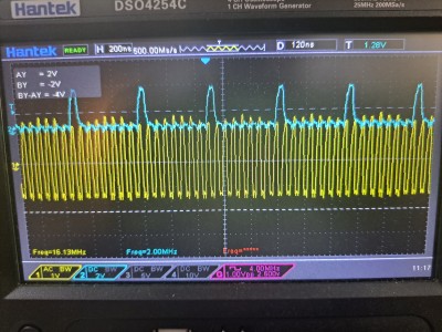
Of course it didn't work first time - it turns out I had omitted the power connection for the CPU - but with that in place it worked perfectly well, at speeds up to 8MHz for both the CPU clock and the I/O clock. Probing some signals revealed that the slew rate on RDY was alarmingly slow:

Attachment:
File comment: Resistors on RDY cause very slow slew rates and limit clock speed
slow_rdy.jpg
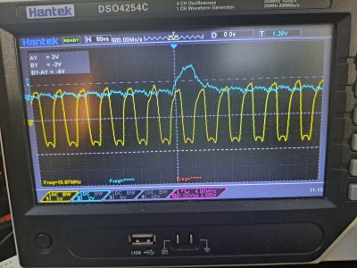
slow_rdy.jpg [ 4.05 MiB | Viewed 28625 times ]


I'd used a rather large resistor there. Downgrading that to 330 ohms helped a lot - it's not a good way to hook it up though, and even a diode with a pull-up resistor doesn't feel much better. It's probably the straw that breaks the camel's back, and I should just stretch the clock instead of using RDY. Anyway, this is working well with a 16MHz clock - I also tried 25MHz as I had that oscillator handy, but it didn't work - not a huge surprise, this prototype was only meant to check the mechanisms were working, not intended to actually run at high speeds.

Attachment:
File comment: Running with a 16 MHz clock, and lots of wait states
waitstates_16MHz.jpg
waitstates_16MHz.jpg [ 4.24 MiB | Viewed 28625 times ]


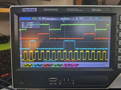
It's worth noting that the CPU isn't really running at that speed because it's constantly waiting for the I/O module. I added more probes to signals along that path to check they were behaving as expected - this shows PHI2 in yellow at the bottom, RDY in blue above it, then IOWAITS in red, and an active-low ACT signal which is where the I/O module performs the actions requested:

Attachment:
File comment: More signals - PHI2, RDY, IOWAITS, ~ACT
phi2_rdy_iowait_act.jpg
phi2_rdy_iowait_act.jpg [ 4.21 MiB | Viewed 28625 times ]


So on the rising edge of PHI2, if the address has the top bit set, RDY is brought low to halt the CPU. The I/O module spots this and synchronizes the signal to its own clock, as IOWAITS, which changes in sync with the slower I/O clock. After one cycle of the I/O clock - to guard against metastability - the I/O module's ~ACT signal is brought low for one I/O clock cycle - and this controls the chip selection for any I/O devices like ROM, VIAs, and the LEDs in the corner. When that signal rises again, it causes the CPU to unpause at the next rising edge of PHI2 and continue execution.

After first I/O cycle shown in the trace above, when RDY goes high again halfway across the screen, it actually stays high for two CPU clock cycles because the next cycle is a RAM access. Then it goes low again, as the code is in ROM and it needs to fetch the next instruction.

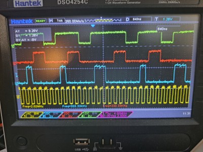
You can see that more clearly here where two instructions in a row both access RAM:

Attachment:
File comment: Two RAM access instructions in a row
two_ram_operations.jpg
two_ram_operations.jpg [ 4.38 MiB | Viewed 28625 times ]


Here, starting with the first peak in RDY (blue), the CPU executes a slow operation from ROM (instruction fetch) so RDY goes low for a while, then high again. Then it executes another one (fetching the operand); then when RDY goes high again, the next bus operation is a RAM access and doesn't require wait states. Then after that it's back to ROM again, fetching another opcode; then an operand; then again it's able to perform a second RAM access without wait states. The instruction sequence here was STA $0 followed by CMP $0 - storing something in RAM and checking it was stored correctly.

Anyway it's working pretty well for a first pass - I'm going to write more involved RAM access tests, testing things like consecutive RAM cycles (JSR, RTS for example), and if that works, make it copy the program from ROM to RAM and run it from RAM. This should flip everything around and we should see the CPU mostly running without wait states, except when it needs to perform I/O accesses (e.g. writing to the LEDs).


Top
 Profile  
Reply with quote  
PostPosted: Wed Aug 02, 2023 2:25 pm 
Offline

Joined: Fri Mar 18, 2022 6:33 pm
Posts: 432
gfoot wrote:
I used KiCad's PCB tool to design a sensible breadboard layout, then built it up this evening - here's the result:

Attachment:
breadboard.jpg


This looks mysteriously familiar... :lol: Great work George! I'm curious what you're planning to use this for. Why do you need totally asynchronous clocks?

_________________
"The key is not to let the hardware sense any fear." - Radical Brad


Top
 Profile  
Reply with quote  
PostPosted: Wed Aug 02, 2023 5:32 pm 
Offline

Joined: Fri Jul 09, 2021 10:12 pm
Posts: 741
Paganini wrote:
This looks mysteriously familiar... :lol: Great work George! I'm curious what you're planning to use this for. Why do you need totally asynchronous clocks?

Thanks! The motivation was just to make a system that can run as quickly as I can, to see how fast it could go and what seems to be the limiting factor (e.g. CPU's overclocking ability, PDIP parts' poor density and pin layouts, etc). It's a design that's broadly been in the back of my mind for a while, and banedon recently posted an "Improving my PCB design" thread (viewtopic.php?f=4&t=7662) which spurred me to go ahead and develop my design more, to see if it would work well.

The only need for asynchronous clocks is to make it simpler to experiment with different CPU clocks without the stability of the I/O system being affected. EEPROMs tend to be rather slow, and the 65C22 VIAs may be less able to overclock than the CPUs for example - using a fixed clock speed for the I/O module removes those from the equation. It also means that code can easily use VIA timers to measure real world times independently of the CPU's clock speed - and with the DS1086Z+ programmable oscillator that Adrien suggested (not a PDIP part but I'm making an exception for this one) the CPU may be able to dynamically change its own clock rate, for no good reason other than it can!

Regarding PCB layout and overall form, this is what I'm planning to build at the moment:

Attachment:
File comment: Render of I/O module, CPU board, VIA board
render-3boards-2023-07-29.jpg
render-3boards-2023-07-29.jpg [ 571.55 KiB | Viewed 28579 times ]


The only bit that matters speed-wise is the CPU module. The three I/O slots have pins essentially matching those on a 6522 VIA, with a couple of extra address lines to allow more than one VIA per module. Other than VIAs, it should easily be able to support things like ACIAs and graphics - I don't know whether I'll ever build any but wanted to have the option. The VIA module can house one or two VIAs and breaks out the I/O pins to four BBC Micro style user port headers. I have a joystick that should plug straight into that.

The I/O module base board includes ROM, an LED bargraph debug port, the reset circuit, and a soft power circuit, and as it's soft-switched I made it automatically power off if an I/O board is inserted backwards, just in case.

I had an earlier layout with all three modules on one 100mmx100mm board, and I might get that built up as well for comparison - while I'm paying for delivery I might as well pay an extra pound for bundling another board design into the order! These are all two-layer boards, and making a four-layer version of the CPU board would be an interesting test to see if it can achieve higher frequencies than the two-layer one. I'm not sure that it'll make much difference though because I was already able to keep a decent ground plane with minimal cuts to it and good return paths for each signal line, especially in the CPU board where it will matter the most. Routing would have been easier, but I feel like the noise reduction benefits of four layer boards are not going to apply much with PDIP parts.


Top
 Profile  
Reply with quote  
PostPosted: Thu Aug 03, 2023 2:34 am 
Offline

Joined: Fri Jul 09, 2021 10:12 pm
Posts: 741
More developments today. I wrote some additional tests to verify that the RAM was working, and copy a small program to RAM and run it from there. That worked really well and you can see here the traces - from bottom to top - of PHI2, RDY, IOWAITS, and ~ACT - the same as in the captures from yesterday.

Attachment:
File comment: Running code from RAM with wait states only for I/O
running_code_from_ram.jpg
running_code_from_ram.jpg [ 5.11 MiB | Viewed 28561 times ]


This shows about 8 cycles running from memory before an I/O operation that causes RDY to drop until the I/O is complete. It's this loop:

Code:
ramcode:
    inx : stx DEBUGPORT
    bra ramcode


I wanted to try using clock stretching instead of RDY in case that allowed running at faster speeds, as I still didn't like the slow transition of RDY. I put a 74AHCT32 "OR" gate between the clock and PHI2, ORring it with the IOWAIT signal that's the opposite of RDY in my circuit - meaning that whenever it's waiting for I/O the CPU's PHI2 is held high. IOWAIT is clocked at the rising edge of PHI2, so lags it a little and won't cause any runt pulses.

This kind of worked but not very well, and I discovered that all this time half my circuit hasn't had a proper power supply! This particular breadboard platter has a lot of breaks in the power rails that aren't marked visibly, so you just have to know where they are and bridge over them. Yuck. The entire bottom two strips had no proper VCC supply - they must have been powered through leakage from other components and signal lines. They did have good ground at least because I ran a ground grid over the whole space first.

With that fixed, things worked better, but the new clock stretching circuit still wouldn't work at 25.175MHz - the oscilloscope showed that at the end of I/O cycles the I/O system was reactivating itself. This was due to the propagation delay of the OR gate delaying the CPU enough that it hadn't sorted out the address bus by the time the crystal clock signal had its rising edge, and the I/O circuit was based on that. I think it's a good way to go but needs a bit more thought, so that the stretched clock and unstretched clock are in sync. I could just pass the unstretched clck through an OR gate as well, but that's ugly! Another 74AHCT139 could probably do a good job of it, or another ATF16V8 - despite the pessimistic datasheet, I'm observing about 5ns propagation delay from clock to output on the one that I'm already using, a full rail to rail output, and about 5ns slew rate, which is better I think than what I've seen from the AHCT parts in general.

Attachment:
File comment: Glitches with clock stretching - I/O cycle "echos"
clock_stretch_glitch.jpg
clock_stretch_glitch.jpg [ 4 MiB | Viewed 28561 times ]


I went back to the RDY-based system though, and with the CPU getting the full 5V rather than about 2.8V that it was getting before, this now runs really well at 25.175MHz. I don't have a wide selection of oscillators, but here's the CPU running at 25.175MHz and the I/O system at 16MHz, showing that the separate clock domains are working OK:

Attachment:
File comment: 25.175MHz main clock, 16MHz I/O clock, running the code-from-RAM test
25MHz_16MHzIO_code_from_ram.jpg
25MHz_16MHzIO_code_from_ram.jpg [ 5.35 MiB | Viewed 28561 times ]


The bottom, yellow line is the CPU clock, the top red line is the I/O clock; the blue line is RDY and the green line is the I/O ~ACT signal.

So that's all very promising - I didn't expect this to run stably on a breadboard at 25MHz.

Something else I started playing with was hooking up a way to boot from SD card. I only have 112 bytes of addressable ROM and it's hard to fit decent programs in that much space. But if I could fit an SD card bootloader, it could load code from there much more flexibly. Unfortunately the smallest I could make viable SD card reading code was about 160 bytes, so quite a lot too big. An interesting challenge nonetheless!


Top
 Profile  
Reply with quote  
PostPosted: Thu Aug 03, 2023 11:33 am 
Offline
User avatar

Joined: Thu Dec 11, 2008 1:28 pm
Posts: 10793
Location: England
Great adventure and great documentation of experiments and progress!


Top
 Profile  
Reply with quote  
PostPosted: Thu Aug 03, 2023 12:44 pm 
Offline
User avatar

Joined: Sat Jul 24, 2021 1:37 pm
Posts: 282
Agreed, really enjoying reading about this experiment.

How did you choose the 330ohms value for the RDY current limiting resistor? The 65C02 datasheet mentions a current of 1.6mA for a low RDY output, which would map to (5.25-0.4)/0.0016 ~= 3k

Did you experiment with putting a capacitor in parallel as Garth suggested here? viewtopic.php?p=89087#p89087

_________________
BB816 Computer YouTube series


Top
 Profile  
Reply with quote  
PostPosted: Thu Aug 03, 2023 12:58 pm 
Offline
User avatar

Joined: Thu May 28, 2009 9:46 pm
Posts: 8144
Location: Midwestern USA
gfoot wrote:
...since I added in the whole I/O module, I couldn't help but make that a bit more fully-featured too...

You might want to put some series resistance into the reset push button circuit. That push button is headed toward an early death due to it directly shorting out a fully-charged capacitor. Suggest you stick 10 to 22 ohms in series with the push button to limit the initial current.

_________________
x86?  We ain't got no x86.  We don't NEED no stinking x86!


Top
 Profile  
Reply with quote  
PostPosted: Thu Aug 03, 2023 1:03 pm 
Offline
User avatar

Joined: Thu May 28, 2009 9:46 pm
Posts: 8144
Location: Midwestern USA
akohlbecker wrote:
Agreed, really enjoying reading about this experiment.

How did you choose the 330ohms value for the RDY current limiting resistor? The 65C02 datasheet mentions a current of 1.6mA for a low RDY output, which would map to (5.25-0.4)/0.0016 ~= 3k

Did you experiment with putting a capacitor in parallel as Garth suggested here? viewtopic.php?p=89087#p89087

Even better is to use a Schottky diode (e.g., BAT85) for isolation and a 3.3K pullup. With that arrangement, when the RDY circuit goes low to initiate a wait-state, response will come in a matter of a few nanoseconds, making timing less critical. Also, with the diode, the transition from high to low will be very fast, unlike the series-resistor, shunt-capacitor arrangement, in which the high-to-low transition is somewhat “lazy.” Both diode and resistor should be as physically close to the MPU as practicable in order to minimize parasitic capacitance.

_________________
x86?  We ain't got no x86.  We don't NEED no stinking x86!


Top
 Profile  
Reply with quote  
PostPosted: Thu Aug 03, 2023 1:19 pm 
Offline
User avatar

Joined: Sat Jul 24, 2021 1:37 pm
Posts: 282
With a diode, the issue is what happens when the RDY input goes from low to high.

With a 3.3k pull up and assuming in the order of 10pF of capacitance on the CPU side, that's an RC constant of 33ns, which is quite close to the half period at 14MHz. Additionally, the source is U5B which has to propagate first from the rising edge of the clock. All in all, this would not satisfy the 10ns setup time on the RDY input of the CPU. Meaning it could register a false wait-state for the next cycle.

EDIT: To be fair, this is also a consideration with a current-limiting resistor, for both transitions, though going for 330 ohms will help make it faster, just like a 330 ohm pull up would!

_________________
BB816 Computer YouTube series


Top
 Profile  
Reply with quote  
PostPosted: Thu Aug 03, 2023 4:06 pm 
Offline

Joined: Fri Jul 09, 2021 10:12 pm
Posts: 741
Thanks for the feedback all!

akohlbecker wrote:
How did you choose the 330ohms value for the RDY current limiting resistor? The 65C02 datasheet mentions a current of 1.6mA for a low RDY output, which would map to (5.25-0.4)/0.0016 ~= 3k

Yes it's not really suitable. I originally had 6k8 I think, for some reason, and I was just trying progressively lower values to improve the slew rate, with 330 being still not very satisfactory but about as low as I was willing to go without checking the datasheet. It was OK in the short term since I wasn't using WAI, intentionally at least! However given the potential for WAI to occur and stay active for a long period, I'm sure it's best not to feed in more current than the CPU would like.

Quote:
Did you experiment with putting a capacitor in parallel as Garth suggested here? viewtopic.php?p=89087#p89087

Ah I'd forgotten about that advice, I might try it later, thanks!

BigDumbDinosaur wrote:
You might want to put some series resistance into the reset push button circuit. That push button is headed toward an early death due to it directly shorting out a fully-charged capacitor. Suggest you stick 10 to 22 ohms in series with the push button to limit the initial current.

Good tip, thanks!

BigDumbDinosaur wrote:
Even better is to use a Schottky diode (e.g., BAT85) for isolation and a 3.3K pullup. With that arrangement, when the RDY circuit goes low to initiate a wait-state, response will come in a matter of a few nanoseconds, making timing less critical. Also, with the diode, the transition from high to low will be very fast, unlike the series-resistor, shunt-capacitor arrangement, in which the high-to-low transition is somewhat “lazy.” Both diode and resistor should be as physically close to the MPU as practicable in order to minimize parasitic capacitance.

I considered it but as Adrien said, I'm concerned about the rise rate as well. In principle it doesn't matter too much if the CPU takes an extra cycle to continue after waiting for an I/O operation, but as things stand my circuit would interpret that as a second I/O operation beginning, because it would still see A15 high at the rising edge of PHI2 with no I/O operation in progress already. So it is currently important that - triggered by the rising edge of PHI2 - U5 resets and the CPU finished the cycle within this clock period.

For me it kind of comes back to RDY not seeming to be a great way to do wait states, as I said in the Woz RDY circuit thread, because there's no way to tell for sure whether the CPU has executed a cycle and begun the next one or not. With a proper stretched clock, you know for sure - either the clock had a low phase, or it didn't. So this morning I tried the stretched clock again, this time with an extra OR gate to try to bring the clock on U5B roughly in sync with the output PHI2's rising edge, especially to give the CPU more time to update its address pins before U5B snapshots the state of A15:

Attachment:
File comment: Changes to use clock stretching instead of RDY
RDY_to_stretching.png
RDY_to_stretching.png [ 19.54 KiB | Viewed 28511 times ]


This is also working fairly well at 25MHz now, but not as well as the RDY circuit was (that one ran for hours this morning running a memory write/read test, without failing). I do prefer this method though and will need to investigate more to see why it's still not as stable. It seems likely that I'll replace these flipflops and OR gates with another PLD, and it will easily be able to handle this more reliably.

Thanks again for all the feedback. I have tested the soft power circuit as well this morning and it needed a few changes, I'll post more details about that later on.


Top
 Profile  
Reply with quote  
PostPosted: Thu Aug 03, 2023 4:28 pm 
Offline
User avatar

Joined: Thu Dec 11, 2008 1:28 pm
Posts: 10793
Location: England
I would be careful about a slowly changing control input, like RDY, because of the risk that some part of the 6502 logic will take it as one and another part as zero, and you would see some kind of malfunction. It's pretty much exactly the same as the crossing of async clock domains - if you can't meet setup and hold times then bad things might happen. And, usually, RDY is time-critical, unlike an interrupt it needs to happen in the cycle that it's supposed to happen, so you can't just retime it with a flop.


Top
 Profile  
Reply with quote  
PostPosted: Thu Aug 03, 2023 5:35 pm 
Offline
User avatar

Joined: Sat Jul 24, 2021 1:37 pm
Posts: 282
I'm also warming up quite a bit to the idea of clock stretching.

I've listed in my other thread all the constraints using RDY adds to the circuit: the need to keep a 65C816's latch closed, and to adapt RD/WR pulses sent to memory... Now, these are all things I've already built into my 65C816 breakout board. However, to make it work and have all the logic and CPU in agreement I had to synchronize the RDY input to the rising edge of the clock. This means that I can't use this edge in circuits generating a RDY_IN signal, which complicates wait states and single stepping quite a bit.

I briefly considered using one of my shifted clock phases (CLK_SRC is advanced from the CLK by around 20ns) as the point where RDY_IN is clocked, freeing up the CLK rising edge. However, the need for a diode or current-limiting resistor make this a non-starter, besides generating an edge at least 50ns in advance, which then limits the frequency.

One thing I'd like to do is see if I can design a clock stretching input that mimics RDY, that doesn't need to be open-collector. So it could be sampled maybe 10 or 20ns before the falling edge of the clock, and solve all those issues.

_________________
BB816 Computer YouTube series


Top
 Profile  
Reply with quote  
PostPosted: Fri Aug 04, 2023 12:04 am 
Offline

Joined: Fri Jul 09, 2021 10:12 pm
Posts: 741
This morning I tested the soft power circuit that was in one of my earlier schematics, I'm not sure whether I posted that one but here it is in its original state:

Attachment:
File comment: Original circuit
softpower-original.png
softpower-original.png [ 18.11 KiB | Viewed 28475 times ]


The idea is that the P-MOSFET (Q1) controls the rest of the circuit's VCC power line. It will only pass current if its gate (pin 1) is held significantly lower than its source (pin 3). IIRC this particular MOSFET is only just usable with a 5V supply - it really needs more than 5V difference to drop its Rds resistance all the way down. But for reasonably low-current applications like this I've found that it's OK. Measuring it in-circuit now with the computer running, its source is at 5.27V and its drain is at 5.24V, so not too much voltage drop, and its gate is at 0.00V.

Its gate is pulled up to the supply rail by R7 (22K), so unless something pulls that low, Q1 won't conduct. Often you'll see an "on" switch going direct to ground here, but I avoided that for reasons I'll explain in a bit. In my case the only thing that can pull down is the other MOSFET, Q2. This one is N-channel, so conducts if its gate (pin 2) is significantly higher than its source (pin 1). 2N7000 is suitable for 5V operation, though again it really wants a bit more Vgs to fully conduct. In this case though 5V is fine, it's only fighting against a 22K resistor, and it wins easily.

So Q1 will conduct if its gate is low, and its gate will be low if Q2's gate is high. The "on" switch pulls Q2's gate up through R8, another 22K resistor. In addition, the main circuit's VCC - which is being switched by Q1 - also pulls Q2's gate up through another 22K resistor, R9. This means that once the circuit is turned on, it latches on.

Once it's latched on, to turn it off we can push the "off" button, which pulls Q2's gate directly to ground. There's also a signal called XSENS there, which is used to cut the power if an I/O card is inserted backwards... kind of a silly thing to add but I guess I felt like it! To do that, one end pin on the I/O card is shorted through to the reverse side of the card edge connector, and on the mainboard if the card is inserted backwards this will short XSENS to ground. The opposite end of the I/O card edge connector has an unconnected pin and a ground pin in these locations.

So that was the theory. In practice, the circuit tended to randomly turn itself on when left in the "off" state for a few seconds. The "off" button could still be used to turn it off, but after a few seconds it would turn on again. I figured some current was leaking through Q1 and down to Q2's gate, which gradually built up a charge until Q2 turned on enough for more current to flow, reinforcing the effect and turning the circuit on. To mitigate this I added a resistor from Q2's gate to ground, so that any such charge would dissipate. I used 22K again here for simplicity and it worked - not ideal though as this resistor and R9 form a potential divider, meaning Q2's gate only ever gets up to about 2.5V, which is not really as high as you'd like, but it still seemed to work well.

The next issue was that capacitance across the power rails in the switched circuit would make it hard to turn off - when you press the "off" button Q1 stops supplying power, but you still need to wait for the capacitors to discharge through R9 and the "off" switch. If you release the "off" switch too soon, it all just turns back on again.

My initial solution for that was to reduce the value of R9 significantly, so that when "off" was pressed it would discharge the capacitors much more quickly. Indirectly this also resolved the voltage divider problem I just mentioned as it meant Q2's gate would sit at a much higher voltage when in the "on" state.

So this was the circuit at that point:

Attachment:
File comment: Added resistor to discharge Q2's gate
softpower-notquitedone.png
softpower-notquitedone.png [ 18.05 KiB | Viewed 28475 times ]


Now the circuit wouldn't turn on! When the "on" switch was pressed, current was meant to flow through R8 and SW2 onto the base of Q2. But R9 is providing an alternate path, and now that its value was much smaller, this led to the following circuit, which didn't bring Q2's gate high enough to turn on Q1:

Attachment:
File comment: Failing to turn on properly
softpower-wontturnon.png
softpower-wontturnon.png [ 10.48 KiB | Viewed 28475 times ]


With SW2 pressed, R8 forms a potential divider with R9 and LOAD (R4 is not very relevant to this). This means that depending upon the resistance of the load, the voltage at Q2's gate might not get very high at all. My fix for this was to put a diode in series with R9, preventing current from flowing "backwards" through it. This leads to the final circuit - or at least, one that seems to work pretty well! As always please do let me know if you think something should be done differently:

Attachment:
File comment: Working circuit
softpower-done.png
softpower-done.png [ 19.44 KiB | Viewed 28475 times ]


One final point that I said earlier I'd come back to explaining - the reason I wanted SW2 to work this way rather than just pulling Q1's gate to ground was that I wanted to make sure that if "on" is pressed while "off" is pressed, or while XSENS is pulled to ground, the circuit would remain off with no current flowing through Q1. The way I have it configured here, that should be the case.


Top
 Profile  
Reply with quote  
PostPosted: Fri Aug 04, 2023 3:28 pm 
Offline

Joined: Fri Jul 09, 2021 10:12 pm
Posts: 741
plasmo wrote:
In this particular case inverted/not-inverted made no difference. viewtopic.php?f=4&t=7433&p=97297&hilit=Overclock#p97297

However, in other cases clock polarity did have 2-3 Mhz difference in top speed. I think it may be interesting to have adjustable duty cycle clock and varying duty cycle of high phase of the clock.

I thought about this a bit today, as if we could have phase 1 last only long enough for the CPU to get its work done, we can go to phase 2 earlier and give the RAM more time for its half of the work, especially in write cycles, as I think Dr Jeffyl noted in his page on clock cycles (https://laughtonelectronics.com/Arcana/ ... iming.html) It may also be possible to shorten read cycles in general compared to write cycles as the RAM has something of a head start in read cycles.

I made a VFO based on Garth's inverter-with-feedback-through-potentiometer design - on solderless breadboard it oscillated stably at 30MHz, but wasn't adjustable. To get a faster speed I replaced the 74HC14 with 74AHCT00 (I didn't have any 74AHC14s), and then with the right tuning it resonated nicely at 150MHz.

Attachment:
File comment: VFO based on 74AHCT00
VFO_74AHCT00.png
VFO_74AHCT00.png [ 7.09 KiB | Viewed 28435 times ]


Like my first attempt, it wasn't adjustable - it was only stable at one frequency, and required tuning the pot to get that stability.

Based on the period of that signal being about 7ns, I figure I could feed it into a counter and arrange for the two phases of the output to have different durations:

Attachment:
File comment: 74ACT163-based variable duty cycle circuit
variable_duty_cycle.png
variable_duty_cycle.png [ 10.69 KiB | Viewed 28435 times ]


However, the counter didn't like the high frequency input signal - either because it's too high or because of the breadboard. Its faster outputs tended to oscillate with 10V-15V peak-to-peak, and when I connected the feedback line from Q2 it settled down but was adding an extra cycle to each half-period, possibly due to setup time issues with /PE. It also overheated at one point.

The variable duty cycle circuit does work fairly well though at lower frequencies. The feedback from Q2 to /PE causes a reload whenever Q2 wraps to low, and we can count up to four cycles at that point before the next reload depending how D0 and D1 are set. The feedback from Q3 to D3 preserves the output level during the reload - note that it already just switched as D2 just carried over. D3 can be fed back into D0 and/or D1 to get different duty cycles on different phases of the output clock, within certain bounds.

Using a separate D flipflop for the output would give a little more flexibility as D0 and D1 could be connected to any of 0V, 5V, OUT, or /OUT, allowing more combinations of half-periods.

I may build this clock generator on perfboard instead, like Garth did, to see if it resolves some of the issues. If I can get more control of it that way and reduce the 150MHz to something the counter is happy to accept then it could be a good way to generate more tailored clock shapes for different scenarios.


Top
 Profile  
Reply with quote  
Display posts from previous:  Sort by  
Post new topic Reply to topic  [ 111 posts ]  Go to page Previous  1, 2, 3, 4, 5, 6 ... 8  Next

All times are UTC


Who is online

Users browsing this forum: No registered users and 23 guests


You cannot post new topics in this forum
You cannot reply to topics in this forum
You cannot edit your posts in this forum
You cannot delete your posts in this forum
You cannot post attachments in this forum

Search for:
Jump to: