6502.org Forum  Projects  Code  Documents  Tools  Forum
It is currently Fri May 10, 2024 5:09 am

All times are UTC


Post new topic Reply to topic  [ 38 posts ]  Go to page Previous  1, 2, 3
Author Message
PostPosted: Thu Aug 03, 2023 10:31 pm 
Offline

Joined: Fri Jul 09, 2021 10:12 pm
Posts: 741
akohlbecker wrote:
On the right, PHI2 is generated from a combination of the input CLK and RDY_IN sampled on the falling edge of CLK_SRC (so 20ns early). The sampling needs to be advanced to give time to the flip flop to propagate. Unfortunately, because the '112 is the only available logic IC I know capable of triggering on the falling edge of the clock, RDY_IN also needs to be inverted, which adds a bit of delay.

Is there some way you can just generate RDY_IN inverted to begin with, to avoid the delay?

I also came across BigDumbDinosaur's thread here - we'd both posted to it so must have read it before, I'm afraid my memory is terrible and I always forget these things. It's worth another look though: viewtopic.php?f=4&t=5229 In particular, if you're already evening-out your clock through a D flip-flop, it looks like an easy way to build in this kind of clock stretching.


Top
 Profile  
Reply with quote  
PostPosted: Fri Aug 04, 2023 2:06 am 
Offline

Joined: Fri Jul 09, 2021 10:12 pm
Posts: 741
I just turned the computer off and then had another thought - is some variation of the standard two-phase non-overlapping clock circuit useful here?

Attachment:
File comment: Standard circuit
20230804_025428.jpg
20230804_025428.jpg [ 1.27 MiB | Viewed 608 times ]


Some examples of letting a RDY-like signal stop the clock:

Attachment:
File comment: RDY via OR gate forces phase 1 immediately
20230804_025437.jpg
20230804_025437.jpg [ 1.6 MiB | Viewed 608 times ]

Attachment:
File comment: RDY via AND gate stops in next phase 2
20230804_025457.jpg
20230804_025457.jpg [ 2.01 MiB | Viewed 608 times ]

Attachment:
File comment: Similar effect but only using NOR gates
20230804_025515.jpg
20230804_025515.jpg [ 1.42 MiB | Viewed 608 times ]


Top
 Profile  
Reply with quote  
PostPosted: Fri Aug 04, 2023 2:40 pm 
Offline
User avatar

Joined: Sat Jul 24, 2021 1:37 pm
Posts: 282
Thanks for the suggestions!

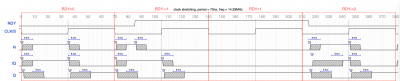
I've looked into the NOR circuit in more details, and built a timing diagram for it. Considering the use of an AHC02 and our pseudo-RDY changing during the low phase of the input clock, we get this:

Attachment:
Screenshot 2023-08-04 at 16.18.22.png
Screenshot 2023-08-04 at 16.18.22.png [ 554.3 KiB | Viewed 583 times ]


It looks like it works well for stretching. Timing is a bit tricky because if it happens to go low when the source clock is already low, a partial PHI2 low is generated (see fourth cycle above).

So, it needs to only change during the high phase of the source clock. Presumably up to right before the edge. I'm not sure if two logic inputs could have different propagations, ie should RDY be setup some nanoseconds before CLK or is 0ns acceptable :?:

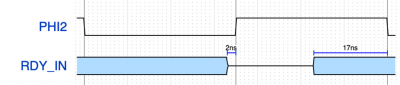
Assuming 0ns is, this is what it looks like from the point of view of Q/PHI2

Attachment:
Screenshot 2023-08-04 at 16.36.30.png
Screenshot 2023-08-04 at 16.36.30.png [ 75.52 KiB | Viewed 583 times ]


So it would need to be stable from 17ns before the falling edge of PHI2, until 2ns before the rising edge of PHI2.

Note that this assumes a very worst case of everything taking either the maximum time to propagate, or the minimum, depending on which edge we're at. In the real world there wouldn't be these massive swings on two consecutive edges for the same IC... But the result is still the same, it needs to be stable a bit before and during PHI2 low.

This is where I'm at, I haven't looked in details into the thread you linked yet, but I will keep thinking about this!

_________________
BB816 Computer YouTube series


Top
 Profile  
Reply with quote  
PostPosted: Sat Aug 05, 2023 11:35 am 
Offline

Joined: Fri Jul 09, 2021 10:12 pm
Posts: 741
akohlbecker wrote:
So it would need to be stable from 17ns before the falling edge of PHI2, until 2ns before the rising edge of PHI2.


Ah yes, it is not as effective as I thought - I think it handles one transition direction well but not the other.

Quote:
So, it needs to only change during the high phase of the source clock. Presumably up to right before the edge. I'm not sure if two logic inputs could have different propagations, ie should RDY be setup some nanoseconds before CLK or is 0ns acceptable :?:

I have experienced problems due to this in a video circuit where I was ORing together two adjacent counter outputs, and when they changed together in opposite directions (quite common of course for a counter!) it caused small dips in the OR gate output, randomly updating some dependent things that were edge-triggered.

Since then I've been more careful to not rely on that - I use a flipflop after the OR gate, or similar methods, to only sample the state of the OR at a time when its inputs aren't in flux, or create overlap between the signals that I'm ORing. I'm probably overcautious about this now.


Top
 Profile  
Reply with quote  
PostPosted: Sat Aug 05, 2023 3:18 pm 
Offline

Joined: Mon Jan 19, 2004 12:49 pm
Posts: 683
Location: Potsdam, DE
gfoot wrote:
I'm probably overcautious about this now.


I don't think it's even possible to be too overcautious when using combinational logic to drive edge-triggered inputs. And even then, I get burned sometimes.

I think life would have been so much simpler if instead of binary counters, they all used gray codes. At least only one bit changes per transition there... of course, sticking a binary-gray code converter after the counter doesn't work, because of the aforementioned edges... :roll:

Neil


Top
 Profile  
Reply with quote  
PostPosted: Sat Aug 05, 2023 10:09 pm 
Offline
User avatar

Joined: Sat Jul 24, 2021 1:37 pm
Posts: 282
gfoot wrote:
I have experienced problems due to this in a video circuit where I was ORing together two adjacent counter outputs, and when they changed together in opposite directions (quite common of course for a counter!) it caused small dips in the OR gate output, randomly updating some dependent things that were edge-triggered.

Since then I've been more careful to not rely on that - I use a flipflop after the OR gate, or similar methods, to only sample the state of the OR at a time when its inputs aren't in flux, or create overlap between the signals that I'm ORing. I'm probably overcautious about this now.


Interesting! Thanks, that's valuable feedback.

_________________
BB816 Computer YouTube series


Top
 Profile  
Reply with quote  
PostPosted: Sat Aug 05, 2023 10:12 pm 
Offline
User avatar

Joined: Sat Jul 24, 2021 1:37 pm
Posts: 282
I've mentioned earlier my idea to trigger this single-stepping circuit using a hardware breakpoint. The idea behind it is to be able to run the computer at full speed, without the impediment of synchronous tracing, while still being very precise in where to pause the execution.

Using a trio of 74HC688 comparators and 74HC595 shift registers (can be reduced to duos for the 6502), and a bit of logic, it is possible for an external system to set and activate a breakpoint triggered at a specific address.

Here is what that could look like:

Attachment:
Screenshot 2023-08-05 at 23.56.54.png
Screenshot 2023-08-05 at 23.56.54.png [ 297.05 KiB | Viewed 534 times ]


During normal execution, /BRK_ENABLE is kept high. When a breakpoint is set, the external system sends it over serial, then it brings /BRK_ENABLE low to enable detection. If the three comparators agree, and breakpoints are enabled, the single stepping circuit is activated.

The '688 propagates in 37ns, and each '32 in 8.5ns, totaling 54ns. With the bank address latch delay, this could be ready around maybe 100ns after the falling edge of the clock. So, unfortunately due to the comparators only existing in the HC family it is not as fast as I would like. A CPLD implementation would be doable quite easily in a small ATF1502 though, or integrated in a larger logic design. Assuming the CPLD already needs the address pins for address decoding, it would only add around 24 flip flops plus 3 control input pins.

_________________
BB816 Computer YouTube series


Top
 Profile  
Reply with quote  
PostPosted: Sat Aug 05, 2023 10:36 pm 
Offline

Joined: Fri Jul 09, 2021 10:12 pm
Posts: 741
CPLD is probably the tidiest solution but you could also use loads of fast XOR gates. XOR is a relatively complex gate but the propagation delay for AHC series is under 10ns. I guess you then need to OR the outputs together - I don't think wide OR/NOR gates are readily available, but you can invert your compare value so that the required operation is an AND, and you can get fast 8-input NAND gates (74AHC30) which are also under 10ns propagation delay. So all together you'd need 16 XOR gates, two 8-input NAND gates, and a 2-input OR gate like 74AHC32, probably 25-30ns worst case propagation delay I think.


Top
 Profile  
Reply with quote  
Display posts from previous:  Sort by  
Post new topic Reply to topic  [ 38 posts ]  Go to page Previous  1, 2, 3

All times are UTC


Who is online

Users browsing this forum: No registered users and 11 guests


You cannot post new topics in this forum
You cannot reply to topics in this forum
You cannot edit your posts in this forum
You cannot delete your posts in this forum
You cannot post attachments in this forum

Search for:
Jump to: