6502.org Forum  Projects  Code  Documents  Tools  Forum
It is currently Thu May 09, 2024 10:51 pm

All times are UTC


Post new topic Reply to topic  [ 32 posts ]  Go to page Previous  1, 2, 3  Next
Author Message
 Post subject: Re: RAM banking
PostPosted: Sat Jul 22, 2023 6:18 pm 
Offline

Joined: Fri Jul 09, 2021 10:12 pm
Posts: 741
It would be easier if you didn't allow reading the register. You can cater for that by having a separate RAM location that code had to update just before changing the hardware register (which is what Acorn did in the BBC Model B, though they provided a readable register in the later Master models) or you can have the hardware register overlay/shadow a RAM address, so that writing the RAM address also writes the hardware register.


Top
 Profile  
Reply with quote  
 Post subject: Re: RAM banking
PostPosted: Sun Jul 23, 2023 7:51 am 
Offline

Joined: Tue Jul 05, 2005 7:08 pm
Posts: 993
Location: near Heidelberg, Germany
Is /banken qualified with phi2? Otherwise it stays valid for too long, and the CPU has taken the data off the bus already
IIRC the 273 latches the data in at rising edge of CP. So you should make sure CP is only low when phi2 is high.

_________________
Author of the GeckOS multitasking operating system, the usb65 stack, designer of the Micro-PET and many more 6502 content: http://6502.org/users/andre/


Top
 Profile  
Reply with quote  
 Post subject: Re: RAM banking
PostPosted: Sun Jul 23, 2023 10:58 am 
Offline

Joined: Tue Jul 05, 2005 7:08 pm
Posts: 993
Location: near Heidelberg, Germany
Good you found the '273 because of its reset capability.

is your /BANKEN qualified with phi2? The '273 latches the value at the rising edge of its clock input, this needs to be at the same time as phi2 going high, otherwise the data might already be lost. You can easily add phi2 to the first stage NAND that you currently use as inverter, to achieve that.

What you need to do is to provide the ability, from kernel mode, to read (and sometimes write) data from (into) the user process. For example reading a file name to open a file is more efficient if the filesystem process can read it from some mapped user space. (you could transfer the name etc using a byte-based protocol with a kernel call per byte, but that is highly inefficient.) Also for reading and writing mass data (like loading a file) the kernel should be able to read from or write to user space.

In GeckOS I have a call buffer per process at a fixed address, that is either shared (in systems without MMU, and protected via a Semaphore), or where the data is in fact copied over into kernel space (system with MMU) with a specific routine (look for PCBUF resp. SYSBUF if I remember correctly). File data transfer is current byte-wise which I think is highly inefficient. I have designed a new interface with block transfers and flexible call buffers, but not yet managed to implemented it.

_________________
Author of the GeckOS multitasking operating system, the usb65 stack, designer of the Micro-PET and many more 6502 content: http://6502.org/users/andre/


Top
 Profile  
Reply with quote  
 Post subject: Re: RAM banking
PostPosted: Sun Jul 23, 2023 12:29 pm 
Offline

Joined: Tue Jul 05, 2005 7:08 pm
Posts: 993
Location: near Heidelberg, Germany
gfoot wrote:
It would be easier if you didn't allow reading the register. You can cater for that by having a separate RAM location that code had to update just before changing the hardware register (which is what Acorn did in the BBC Model B, though they provided a readable register in the later Master models) or you can have the hardware register overlay/shadow a RAM address, so that writing the RAM address also writes the hardware register.


It would be easier, but not necessarily better. Esp. if you do multitasking sometimes it is just easier reading from a register and save the value when another task is started, and restore it from there when coming back. That is not necessarily the case with the banking register though.
For example, in the 8x96 Commodore PET, they had a banking register "under" the ROM at $fff0. It was only writable. So this works, but depending on the purpose of the register you may want to re-think that.

Here you have to check with your software design if you could spare some storage (a byte) for the current bank if you can just read the value from the register when going from user space to kernel.

_________________
Author of the GeckOS multitasking operating system, the usb65 stack, designer of the Micro-PET and many more 6502 content: http://6502.org/users/andre/


Top
 Profile  
Reply with quote  
 Post subject: Re: RAM banking
PostPosted: Sun Jul 23, 2023 2:18 pm 
Offline

Joined: Tue Jul 05, 2005 7:08 pm
Posts: 993
Location: near Heidelberg, Germany
As long as the forum issue is not fixed (a couple of posts disappearing between page 1 and 2) you may want to use this link that shows the missing posts (thanks to @Ed for providing it) viewtopic.php?f=4&t=7591&start=11

Edit: fixed link

_________________
Author of the GeckOS multitasking operating system, the usb65 stack, designer of the Micro-PET and many more 6502 content: http://6502.org/users/andre/


Top
 Profile  
Reply with quote  
 Post subject: Re: RAM banking
PostPosted: Sun Jul 23, 2023 5:08 pm 
Offline
User avatar

Joined: Fri Feb 17, 2023 11:59 pm
Posts: 163
Location: Lviv, Ukraine
fachat wrote:
Good you found the '273 because of its reset capability.
[...]
Is /banken qualified with phi2? Otherwise it stays valid for too long, and the CPU has taken the data off the bus already
IIRC the 273 latches the data in at rising edge of CP. So you should make sure CP is only low when phi2 is high.


Yep, it is: I have used /RD & /WD signals (qualified with Ф2) as inputs in my latest design, since I already have them in my SBC. I also happened to have just enough spare '14 gates for this task:

Attachment:
rw_banking3.jpg
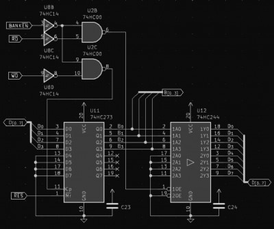
rw_banking3.jpg [ 101.46 KiB | Viewed 4559 times ]


gfoot wrote:
It would be easier if you didn't allow reading the register. You can cater for that by having a separate RAM location that code had to update just before changing the hardware register (which is what Acorn did in the BBC Model B, though they provided a readable register in the later Master models) or you can have the hardware register overlay/shadow a RAM address, so that writing the RAM address also writes the hardware register.


While I agree that it would eliminate the need in '244, I still prefer to use it for two reasons: it gives me satisfaction to do hardware solution for this and it also eliminates the need to track a copy of last written value in RAM.

fachat wrote:
What you need to do is to provide the ability, from kernel mode, to read (and sometimes write) data from (into) the user process. For example reading a file name to open a file is more efficient if the filesystem process can read it from some mapped user space. (you could transfer the name etc using a byte-based protocol with a kernel call per byte, but that is highly inefficient.) Also for reading and writing mass data (like loading a file) the kernel should be able to read from or write to user space.


Yeah, it seems like it would be nice to have an ability to map different regions of multiple banks at once, especially when there's a need to copy data between processes, or work with kernel & user-space data simultaneously.
Another option I can think of is to use "swap" memory for this purpose, e. g. during some syscall, a kernel would copy data from bank 1 into this area, then switch to bank 2 and copy the data there.
But I think most of this copying can be minimized if all program-related data (file descriptors, buffers, etc) is to be stored in program bank. In other words - make kernel use program banks as much as possible, and use kernel's own bank only for metadata (process list, etc). This way each program will "own" most of its data locally. There are some complications though: a program should never touch those kernel-managed data regions of its bank, and mutate them only via syscalls. And, of course, copying data between banks will be very slow.

André - would you mind providing some link or code for your call buffer feature? It sounds interesting and I'm really interested in understanding how it works. Is it just a shared region of memory to be used by multiple processes to transfer data between banks, or something more complex?

_________________
/Andrew

deck65 - 6502 slab with screen and keyboard | ПК-88 - SBC based on KM1810VM88 (Ukrainian i8088 clone) | leo80 - simple Z80 SBC
nice65 - 6502 assembly linter | My parts, footprints & 3D models for KiCad/FreeCAD


Top
 Profile  
Reply with quote  
 Post subject: Re: RAM banking
PostPosted: Sun Jul 23, 2023 5:46 pm 
Offline
User avatar

Joined: Wed Feb 13, 2013 1:38 pm
Posts: 586
Location: Michigan, USA
and3rson wrote:
Yeah, it seems like it would be nice to have an ability to map different regions of multiple banks at once, especially when there's a need to copy data between processes, or work with kernel & user-space data simultaneously.

I was looking at the 74HC670 4-bit Register File IC some years back for the ability to map different segments into 64K address space. I had seen the '670 used in projects by the RC2014 Z80 crowd. Could something like that be useful in your project? *drawing below was for an '1802 project which uses separate address space for I/O...

Good luck on your project.


Attachments:
K8LH MMU excerpt.png
K8LH MMU excerpt.png [ 236.39 KiB | Viewed 4555 times ]
Top
 Profile  
Reply with quote  
 Post subject: Re: RAM banking
PostPosted: Sun Jul 23, 2023 6:19 pm 
Offline
User avatar

Joined: Fri Feb 17, 2023 11:59 pm
Posts: 163
Location: Lviv, Ukraine
Michael wrote:
I was looking at the 74HC670 4-bit Register File IC some years back for the ability to map different segments into 64K address space. I had seen the '670 used in projects by the RC2014 Z80 crowd. Could something like that be useful in your project? *drawing below was for an '1802 project which uses separate address space for I/O...


'670 looks cool - I think I saw your picture earlier, but failed to realize the convenience of it! I also saw something similar in André's articles about MMU, though seems like it was '610.

I think I could wire my A11-A14 to inputs (D0-D3) and use its outputs (Q0-Q3) as A15-A18 for RAM. For writing the file however, I think I'll need to use '157, since new values will come from data bus. Something like this:

Code:
             +------+      +------+
A11-A14 ---> |      |      |      |
             | '157 | ---> | '670 | ---> A15-A18 (RAM)
D0-D3   ---> |      |      |      |
             +------+      +------+


As a result, I'll have 16x 32KB banks in RAM, each divided into 16x 2KB regions that can be mapped individually.

Since it seems that '670 doesn't have a reset input, the kernel would be responsible for initializing it on boot.

EDIT: I think I messed up a bit: '670 is a 4-word file, not 16-word... So I can only have 4x 8KB regions mapped individually, not 16:

Code:
             +--------+                +--------+
D4-D5   ---> | A      |                | '670   |
             |      Y | -------------> | Wa, Wb |
A13-A14 ---> | B      |                |        | ---> RAM
             |  '157  |       D0-D3 -> | D      |
             |        |                |        |
REG/WR\ ---> | ~A/B   |     REG/WR\ -> | ~Gw    |
             +--------+                +--------+

'157 selects D4-D5 when REG/WR\ asserted, A13-A14 otherwise.
'670 latches D0-D3 to word from '157 when REG/WR\ is asserted, otherwise it selects RAM bank.

To map Xth 8-KB segment to bank Y:

D5..D4  = X (0..3)
D3..D0  = Y (0..15)
REG/WR\ = asserted

_________________
/Andrew

deck65 - 6502 slab with screen and keyboard | ПК-88 - SBC based on KM1810VM88 (Ukrainian i8088 clone) | leo80 - simple Z80 SBC
nice65 - 6502 assembly linter | My parts, footprints & 3D models for KiCad/FreeCAD


Top
 Profile  
Reply with quote  
 Post subject: Re: RAM banking
PostPosted: Sun Jul 23, 2023 8:16 pm 
Offline

Joined: Fri Jul 09, 2021 10:12 pm
Posts: 741
I can't remember whether I already posted this, I thought I had but can't see it, so sorry if it's repeating, but in my experiment with this sort of thing I put some normal static RAM between the PID register and the high address lines of my main memory so that each process had its own page table. Processes used a system call to request pages to be mapped, and the supervisor (PID=0) can map any pages it likes for itself including those already used by other PIDs, so it can read memory of other processes if necessary.

In the prototype I only used 32K of main memory, so not many address lines were used, but it would scale up well to larger RAM modules - or the high bits in the page table could reflect executability and other protection states. At some point you might want 16 data bits in the page table. I probably copied most of these ideas from Andre's system.

Attachment:
5530451601220609552.png
5530451601220609552.png [ 79.71 KiB | Viewed 4526 times ]


Top
 Profile  
Reply with quote  
 Post subject: Re: RAM banking
PostPosted: Sun Jul 23, 2023 8:21 pm 
Offline

Joined: Tue Jul 05, 2005 7:08 pm
Posts: 993
Location: near Heidelberg, Germany
@gfoot how do you set the pagetable values? Wouldn't it require some registers visible to the CPU? That seems to be missing or I haven't understood how it works

_________________
Author of the GeckOS multitasking operating system, the usb65 stack, designer of the Micro-PET and many more 6502 content: http://6502.org/users/andre/


Top
 Profile  
Reply with quote  
 Post subject: Re: RAM banking
PostPosted: Sun Jul 23, 2023 8:49 pm 
Offline

Joined: Fri Jul 09, 2021 10:12 pm
Posts: 741
fachat wrote:
@gfoot how do you set the pagetable values? Wouldn't it require some registers visible to the CPU? That seems to be missing or I haven't understood how it works

For the supervisor process I think it was memory-mapped, with user processes using a syscall to request maps be set up for them.

On the hardware side I think ideally you'd use some transceivers or multiplexers to control the buses to the pagetable RAM, but I didn't get that far, this prototype was very hacky and I seem to remember I cut a lot of corners on that bit. It's no harder than the way video RAM is shared between the CPU and GPU though - you just need to make the address decoding swap things around when you're writing to the pagetable.


Top
 Profile  
Reply with quote  
 Post subject: Re: RAM banking
PostPosted: Mon Jul 24, 2023 5:13 am 
Offline

Joined: Tue Jul 05, 2005 7:08 pm
Posts: 993
Location: near Heidelberg, Germany
You may want to look at how I replaced the 74ls610 with some fast RAM.
http://www.6502.org/users/andre/hwinfo/ls610/index.html

_________________
Author of the GeckOS multitasking operating system, the usb65 stack, designer of the Micro-PET and many more 6502 content: http://6502.org/users/andre/


Top
 Profile  
Reply with quote  
 Post subject: Re: RAM banking
PostPosted: Fri Aug 18, 2023 9:42 pm 
Offline
User avatar

Joined: Fri Feb 17, 2023 11:59 pm
Posts: 163
Location: Lviv, Ukraine
Thank you for your responses!

Andre, Michael - '610 seems to be the perfect solution. And I don't even need a '157 in front of it - it's already a simple self-sufficient MMU.

Attachment:
v2_0_banking_610.jpg
v2_0_banking_610.jpg [ 121.71 KiB | Viewed 4386 times ]


This gives me 16x 32 KB banks with my AS6C4008 RAM, each divided into 4x 8KB sub-banks that can be mapped individually.

With BANK/WR asserted by access to $D000-$DFFF, I can configure 4x 8 KB banks by writing to one of four registers:

- $D000 - select bank for CPU address range $0000-$1FFF (region 1)
- $D001 - same for $2000-$3FFF (region 2)
- $D002 - same for $4000-$5FFF (region 3)
- $D003 - same for $6000-$7FFF (region 4)

To read those registers, some more glue logic is required, but this is already a good start, since my kernel will be able to efficiently copy data between banks.

However I'll probably use region 4 to keep track of active bank mappings as well as kernel's own stuff and shared memory.

The only downside is whenever I'm context-switching between processes, 3 writes are needed to swap first 3 regions from one process memory to another.

_________________
/Andrew

deck65 - 6502 slab with screen and keyboard | ПК-88 - SBC based on KM1810VM88 (Ukrainian i8088 clone) | leo80 - simple Z80 SBC
nice65 - 6502 assembly linter | My parts, footprints & 3D models for KiCad/FreeCAD


Top
 Profile  
Reply with quote  
 Post subject: Re: RAM banking
PostPosted: Sun Aug 20, 2023 1:26 pm 
Offline
User avatar

Joined: Fri Feb 17, 2023 11:59 pm
Posts: 163
Location: Lviv, Ukraine
I tried to go below 3 chips for full read-write ability for banking registers, but this is best I could do.

Attachment:
rw_banking4.jpg
rw_banking4.jpg [ 198.46 KiB | Viewed 4347 times ]


'157 selects A0-A1 when bank index register is accessed (to read/write bank index for each of 4x 8KB regions), and A13-A14 when bank is accessed.
'670 stores 4-bit bank index for each of 8KB registers.
'244 puts bank index on data line when bank index register is read.

_________________
/Andrew

deck65 - 6502 slab with screen and keyboard | ПК-88 - SBC based on KM1810VM88 (Ukrainian i8088 clone) | leo80 - simple Z80 SBC
nice65 - 6502 assembly linter | My parts, footprints & 3D models for KiCad/FreeCAD


Top
 Profile  
Reply with quote  
 Post subject: Re: RAM banking
PostPosted: Sun Aug 20, 2023 5:12 pm 
Offline
User avatar

Joined: Wed Feb 13, 2013 1:38 pm
Posts: 586
Location: Michigan, USA
richardc64 had an interesting solution in this post using a pair of '670s sharing the same I/O addresses.


Top
 Profile  
Reply with quote  
Display posts from previous:  Sort by  
Post new topic Reply to topic  [ 32 posts ]  Go to page Previous  1, 2, 3  Next

All times are UTC


Who is online

Users browsing this forum: No registered users and 7 guests


You cannot post new topics in this forum
You cannot reply to topics in this forum
You cannot edit your posts in this forum
You cannot delete your posts in this forum
You cannot post attachments in this forum

Search for:
Jump to: