ISAC --a chip for the 6502 on ISA

For discussing the 65xx hardware itself or electronics projects.
User avatar
wayfarer
Posts: 191
Joined: 19 Mar 2023
Location: about an hour outside of Springfield

ISAC --a chip for the 6502 on ISA

Post by wayfarer »

ISAC is a standalone address decoder IC for the 8-bit ISA bus built for the 6502.
ISAC provides a variety of features and integrates to the 6502 offering:
  • Bus Mastering
  • DMA Channels and Block Transfers
  • IRQ Priority Sorting and Routing
  • Address Bank Switching for up to 1MiB of address space
  • ISA bus expansion slots.
  • Device to Device Messaging
  • Vector Shadowing and Redirection
ISAC/ISAAC stands for Industry Standard Architecture (Addressing) Controller
ISAC is based on a modified 6522 and uses 6502 compatible commands and signaling.
if possible, relocatable memory mirroring/shadowing may be implemented.

So we are drawing from the Intel ISA bus specification (8bit) and the IEEE P996 standard that never really got off the ground.
We are making a few declarations here, and stating some deviations from these standards:

We are probably making the bus speed faster for our systems, though this will be looked into further. ISAC may run faster than the cpu, as fast as the cpu, or on some other multiplier that syncs to the system.

The OSC pin is stated to be 14.xyz Mhz, which divides down to an old standard we are not using, therefore, we might be commandeering the OSC line as an oscillator line, with a BIOS look up of the frequency used, more research needs to be done to determine if other cards would be damaged by this change or if they can be ignored. I would say, for the ISAc chip itself, this might be 'user definable' and users or vendors can comply with whatever they choose.

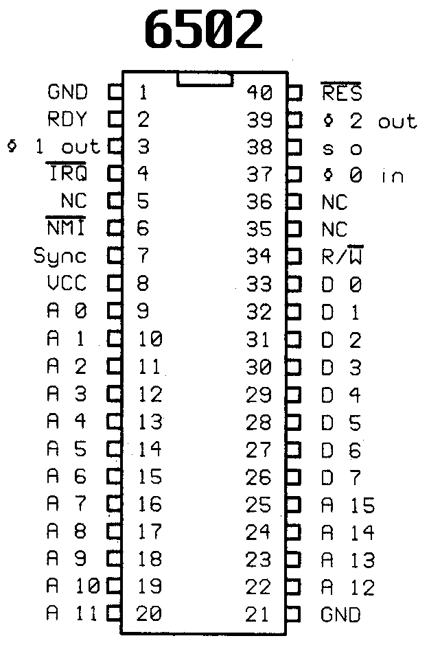
According to P996, ISAC is the Permanent Master of the bus, as it has the highest bus-width. A 6502 (or 6502/6522 module similar to the W65C122S) may become the Alternative Master, until such time as a full bus width CPU module could be formed and assume these duties.

so at this point we are strictly 8bit by design.

so far I have seen the 1MiB broken up into 16 64k regions repeatedly, and those regions referred to as: Banks, Segments, and Pages, the last of which I abhor that should be about 256 or 512 words imo. Id almost call them books, though I digress. This is a logical system of arrangement as the cpu/mpu module at this point, accesses 64k of address space at a time.

ISAc will need to keep track of the several things:
  • Id like 256 4K nodes on a table that map to how they are protected, mapped, assigned etc.
  • So this is 4 bits 'internal' to each Book/Bank/Slot, and 4 bits external to each one, to provide 256 4K nodes across 1MiB of space.
  • Where the cpu, or other devices are currently mapped to,
  • the return paths for the cpu (or other devices)
  • given limited register space in current cplds (ATF150x, ispMAX4000, etc), storing the return state of the cpu is difficult
  • ram/device echo or shadowing tables
    if the cpu is accessing Book A, and Book A doesnt have a RAM chip available to use as zero page and stack, then the cpu
    would know this and only have the ability to use "shadowed RAM" from Slot 0 (or elsewhere) instead of local ram in that slot.
  • what devices are using what slots, at any given time
  • irqs between devices and cpu
  • dreq and dack signaling
  • its own microcode/state-machine
For instance, a system might be designed so that the first four Slots after 0, Slot 1,2,3,4, are Program Slots, and have lots of ram, the control and reset vectors all mapped correctly and so far as the cpu knows, thats the only 64k of address that exist. Then, through a control register, one could "swap slots" and the cpu would be updated to run from that Slot, as if it were native. there are other arrangements, and these 'Slots' might all exist in one big RAM chip, controlled by ISAC.

it is very possible we will use a 6404 as the active controller. it should be able to easily address and control and 6522, or part of one, as well as all low bit protocols.

https://docs.google.com/spreadsheets/d/ ... id=0#gid=0

List of Resources
https://ist.uwaterloo.ca/~schepers/MJK/6502.html
https://allpinouts.org/pinouts/connectors/buses/isa/
https://www.vogons.org/viewtopic.php?t=102338
viewtopic.php?f=1&t=7178
viewtopic.php?f=1&t=1525&p=93118#p93118
https://standards.ieee.org/ieee/896.1/1268/
https://ia804607.us.archive.org/25/item ... 2_text.pdf
http://bos.asmhackers.net/docs/dma/docs/dma0.php.htm
http://bos.asmhackers.net/docs/dma/docs ... ma.php.htm
https://www.retrobrewcomputers.org/lib/ ... sa-bus.pdf

http://www.brokenthorn.com/Resources/OSDev21.html

so in the section here on the 8257,
Quote:
We have the gerneric address lines, A0-A7, which connect to the systems address bus. During inputs, the CPU is only able to write data to A0-A3 to select registers to read from. All pins are used for outputs (to a physical memory address) but are only activated during a DMA request. Last but not least is the generic D0-D7 pins that connect to the systems data bus.
so if there are 4 address lines here, I see these as the upper 4 address lines that control the 16 banks, and the other 4 lines as similar to the 6522 register select lines. For now we can consider that as a remap so far. so, the 4 RS lines on the 6522 stay the same (and we might have additional registers or replace them if needed. The other 4 address lines are the external A16-A19.


History
Quote:
as stated by Proxy here: viewtopic.php?f=4&t=7274#p99779
Proxy wrote:
ISA on a 65c02 is gonna be a bit difficult. as ISA requires 1MB of Address space, while the 65c02 can only handle 64kB. so you some hardware to bank the ISA bus into a smaller section (like 4kB or 8kB), which of course also makes it much slower.
meanwhile the 65816 can easily handle the whole bus with it's 16MB of Address space.
6502ISA.png
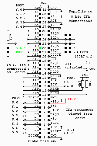
I was just getting started here and it is easy to see, yes, there are 4 address pins "free" on the ISA buss compared to the 6502 available memory. so, what to do with them?
I am of a mind to use them as 'chip select' or 'bank select' and I am ok to burn a few clock cycles to change 'upper address bits with a 4 bit register' and have 16 times the normal ram. or address space. context switching, dedicated devices etc.
[*]leave unused
[*]bank or device switching
[*]use a delayed read/write operation to use an external register for the extra bits
I have Intel ISA Spec 2.01 Sep 89, It does say a Maximum of 1MB. (section 6.1)
In several other places it says, 8 bit cards use 64K, (section 6.2) and in other places (add on card focus) that only 10 address lines are used traditionally. ISA was intended by Intel to use their 8259A, and so unless we try to implement that exactly, we are going to diverge a little. in 6.3 and further it says that data is moved in 8 or 16 bit transfers. I think "using ISA" for a 6502 is probably a worthy experiment.
The primary goal here in not necessarily to use the physical ISA hardware, though that is highly appealing as it is off-the-shelf components. PC/104 and PCMCIA however are both built on top of ISA and getting it established is for the moment, as good of a buss to use as any, primarily due to future connectivity with existing standards.
so what other thoughts are there on a 6502 using an ISA physical connector or design specification (since they exist and it is well documented). a 65816 is clearly more suited to this as Rob Finch has developed such a system. what caveats and considerations are there for the ISA bus?
Last edited by wayfarer on Mon May 19, 2025 12:44 am, edited 10 times in total.
User avatar
Proxy
Posts: 746
Joined: 03 Aug 2018
Location: Germany

Re: 6502 on ISA

Post by Proxy »

well you likely don't want to connect all 16 CPU address lines to the bus as that would fill the entire address space with ISA, leaving nothing for RAM, ROM, or dedicated IO.
that's why i suggested a smaller window so you can still use the rest of the system normally without having to use ISA Cards to get some RAM/ROM (though that would also be an option).
if you only connect A0-11 from the CPU it would give you a 4k window, and the remaining 8 address lines (A12-19) could be controlled from a VIA or similar IO register.
and that also ignores the fact that you have to generate the IOR/IOW and MEMR/MEMW signals, which would likely be handled by some decoing logic. plus some wait state logic since i doubt ISA Cards would work at +10MHz without any wait states.
there is also the issue of seperate IO and Memory Access. you could do it with another pin from a VIA, or with a CPU Address pin.
so your 4k window would be mirrored in memory, accessing one would count as an "IO" access and the other as "Memory". though using the VIA would save you 4k of memory.

another small problem is the BIOS ROM that some cards have on them, which usually contain code and data to initialize and use the card. of course x86 assembly won't run a 65C02, which either means avoiding such cards or disassembling the ROM and replicating it's function in 6502 assembly.
the second option could be kinda automated if you have some form of storage device. since you could have the CPU scan the ISA bus for any ROMs that might have matching 6502 replacements which could be loaded from storage.

either way i'd be interested to see how this could perform. being able to use ISA Cards would be pretty damn cool.
User avatar
wayfarer
Posts: 191
Joined: 19 Mar 2023
Location: about an hour outside of Springfield

Re: 6502 on ISA

Post by wayfarer »

certainly.

http://www.6502.org/users/mycorner/6502 ... sa/isa.png

a lot of what I am doing is echoed by lee davison, echoed here on 6502.org

http://www.6502.org/users/mycorner/6502/suprchips/isa/

he just tied the top 4 pins to ground...

I will stick with it as I go.

I am thinking of using a board controller to hand a lot of this off to,

in simple terms, I think a latch (and Im guessing a driver) could hold the chip select/enable bits, and upper 4 address bits, mapped to a vector/memory location, so on the next cycle it would fill in the top byte

to me, this makes sense if you set them, do a lot of stuff, and change them again and use zero page and stack to move between upper and lower ranges.
if, they get used at all, I think a basic on this board, on expansion board, somewhere on a cable, or maybe different speed protocols, idk yey, accessing those upper 4 bits, it really just an 'extra' for later, plenty with 16 bits as is :)
User avatar
wayfarer
Posts: 191
Joined: 19 Mar 2023
Location: about an hour outside of Springfield

Re: 6502 on ISA

Post by wayfarer »

Proxy wrote:
well you likely don't want to connect all 16 CPU address lines to the bus as that would fill the entire address space with ISA, leaving nothing for RAM, ROM, or dedicated IO. that's why i suggested a smaller window so you can still use the rest of the system normally without having to use ISA Cards to get some RAM/ROM (though that would also be an option).
if you only connect A0-11 from the CPU it would give you a 4k window, and the remaining 8 address lines (A12-19) could be controlled from a VIA or similar IO register.
well, what you have, is everything is already on a bus, and following this arrangement, can conform to ISA.
consider if you add a 4 bit decoder (or use a 6509/6809) you are at 1MB anyway. from what i have heard, this led to some problems.
i am saying, using this standard, and adhering to this protocol/specification. Please do not confuse 'having an isa slot' with using the isa bus system. so for our purposes, each bit of our 4bit decoder gives us a full 64k 'bank', similar to an NES memory map controller (MMC).
so, rather than 'leave some pins for isa, some pins for cpu, etc', we have 16 banks of 64k arranged on the 8bit ISA bus. And the can refer to each other using the upper 4 bits of extended space. 00000-0FFFF is the main cpu, and you might have an ISA slot on A0000, B0000 and C0000, with a bank for peripheral control on D0000, nothing but 64k of RAM in E0000 and use F0000 as a bios ROM, all at 64k each. and all of them able to access each other through the DMA controller.
Quote:
and that also ignores the fact that you have to generate the IOR/IOW and MEMR/MEMW signals, which would likely be handled by some decoing logic. plus some wait state logic since i doubt ISA Cards would work at +10MHz without any wait states. there is also the issue of seperate IO and Memory Access. you could do it with another pin from a VIA, or with a CPU Address pin. so your 4k window would be mirrored in memory, accessing one would count as an "IO" access and the other as "Memory". though using the VIA would save you 4k of memory.
so yes, a cpld here is probably enough, though an fpga or mcu as a dma controller is a thought, as is multiple VIAs. multiple vias, multiple 6502s are a thought to stay 'in family' and simplify things. to address this concern however, some kind of isa buss and dma controller will be used, though we are thinking 'each device does its dma' and we just gate or direct it for timing.
Quote:
another small problem is the BIOS ROM that some cards have on them, which usually contain code and data to initialize and use the card. of course x86 assembly won't run a 65C02, which either means avoiding such cards or disassembling the ROM and replicating it's function in 6502 assembly. the second option could be kinda automated if you have some form of storage device. since you could have the CPU scan the ISA bus for any ROMs that might have matching 6502 replacements which could be loaded from storage.
either way i'd be interested to see how this could perform. being able to use ISA Cards would be pretty damn cool.
Im not trying to make every ISA card work on a board with ISA slots, that has a 6502, its just too far outside the scope of this.

what i am trying to do is, use the ISA standard as a format for a system buss for the 6502, peripherals, expanded address spacing, dma, inter-device communication and multiprocessor banking. totally appreciate what you are saying here Plasmo, I do not want to say 'im not putting isa slots on a board with a 6502' or 'you cant use isa cards on this system from antiquity', those are totally possible. I am just not making "ISA next to a 6502 it can talk to", I am saying "I am using the ISA a bus as a system bus, and the first 64k of it is the main 6502, and the rest of the 1MB address space is done by manipulating vectors/registers/address locations with data, through the cpld type system extender ISA-MMC mapper chip. :D
User avatar
wayfarer
Posts: 191
Joined: 19 Mar 2023
Location: about an hour outside of Springfield

Re: 6502 on ISA

Post by wayfarer »

so for this ISACoder, we are looking at making the 4bit bus extender CPLD, also a DMA handler and IRQ priority handler.
we may involve a 6522 here, though would prefer to keep costs down hardware wise

https://cires1.colorado.edu/jimenez-gro ... entals.pdf

https://www.robots.ox.ac.uk/~adutta/blo ... _desc1.jpg

https://ist.uwaterloo.ca/~schepers/MJK/pics/6502.gif

https://bitsavers.org/pdf/intel/_busSpe ... _Sep89.pdf
BruceRMcF
Posts: 388
Joined: 21 Aug 2019

Re: 6502 on ISA

Post by BruceRMcF »

wayfarer wrote:
... I am just not making "ISA next to a 6502 it can talk to", I am saying "I am using the ISA a bus as a system bus, and the first 64k of it is the main 6502, and the rest of the 1MB address space is done by manipulating vectors/registers/address locations with data, through the cpld type system extender ISA-MMC mapper chip. :D
Where is the code that is manipulating vectors/registers/address locations? It also must residing in the logical address space of the 6502.

Now, you can have a relatively "big" bank rather than a small one, but the top of the logical address space holds the reset and interrupt vectors, and there has to be a vector for the reset to work to start up the chip, so it is conventional to have ROM living starting from the top.

And the Zero page and Stack pages have have at least some RAM, so it is conventional for the RAM to live starting at the bottom.

Three different workable logical memory maps come to mind:

(1) Biggest possible extended bank, 32KB. RAM from $0000-$3FFF, extended bank from $4000-$BFFF, ROM from $C000-$FFFF.

(2) Flexible multiple RAM / ROM / I/O access as above, but 16KB extended banks from $4000-$7FFF and $8000-$BFFF.

(3) Shrink the boot-up spaces to get 3 16KB extended banks: 8KB power up RAM, $0000-$1FFF, BANK1 at $2000-$5FFF, BANK2 at $6000-$9FFF, BANK3 at $A000-$DFFF, Boot-up ROM at $E000-$FFFF.

In any event, latches addresses at $0000, $0000/$0001 or $0000/$0001/$0002 might be used to provide the missing 5 or 6 bits for their extended address.

It is all much cleaner with a 65816. 32KB of RAM from $000000-$007FFF, 32KB of ROM at $008000-$00FFFF and extended bus space at $010000-$10FFFF.
User avatar
wayfarer
Posts: 191
Joined: 19 Mar 2023
Location: about an hour outside of Springfield

Re: 6502 on ISA

Post by wayfarer »

ok, so for some clarity on the way I am planning to use this, please see the thread here on the modern gaming specification:
viewtopic.php?f=4&t=8354

so the address space you all keep referring to, is Bank 0
You get 15 more give or take.
BruceRMcF
Posts: 388
Joined: 21 Aug 2019

Re: 6502 on ISA

Post by BruceRMcF »

wayfarer wrote:
ok, so for some clarity on the way I am planning to use this, please see the thread here on the modern gaming specification:
viewtopic.php?f=4&t=8354

so the address space you all keep referring to, is Bank 0
You get 15 more give or take.
But the 65C02 logical address space is always $0000-$FFFF, not matter that the address decode circuitry can decode $000000-$0FFFFF.

If you have an IRQ swapping to "space 5", with the high four bits of the bus set to %0101, then the status register and return address are pushed onto the stack in $050100-$0501FF, and the free space on the stack is at the physical address $050100,S. Whatever vectors or other information that existed at $00000-$000FF disappear from the "view" of the 65C02, and are replaced by the page at the physical address $050000-$0500FF. The interrupt and reset vectors are addressed by the CPU at $FFFA-$FFFF are at the physical addresses $05FFFA-$05FFFF.

So if you swap the 15 other 64KB address spaces as 64KB banks, then each of those banks have to be a free standing workspace and codespace for the CPU and IRQ, BRK and RESET vectors near the top.

If one 64KB bank is peripherals, then the code accessing the peripherals has to be in that bank, and any RAM workspace or stack space has to be available in that bank. And any call into that bank can only carry the information in the A, X and/or Y register.

If, instead, you map the logical address space $4000-$BFFF to one of 32 32KB bank at $(BANK*32K)+(Logical_Address-16K), the zero page, stack page, and interrupt vectors don't all disappear when the banks change.

The reason that 65C816 can pull the 64KB Bank trick is because it always accesses the "direct page" in bank 0, always accesses the stack in Bank 0, and always accesses the interrupt vectors in Bank 0. It supports having a 64KB Bank of peripherals without any code to execute and without any RAM workspace in that part of the physical address space, since it can execute code from one bank, use another bank for 64KB data addresses, and still access the direct page and the stack on Bank 0 for RAM workspace for the code.

So, again, if you are committed to 64KB banks in a 1MB extended workspace, then it'd be better to use the 65816, which by its design is able to cope with that kind of environment. You can have ISA space be all of the space that can be accessed, so long as you set up ISA $000000-$00FFFF to work as Bank 0 for the 65816. 32KB RAM at the bottom of Bank 0 and and 32KB Flash ROM at the top of Bank 0 would be perfectly fine for that.

Or if you prefer more flexibility in what ISA Bank 0 is, you could have the 65816 Bank 0 with its boot ROM and Stack/Direct page RAM as an "internal CPU resource", and map banks 1-15 directly, ($010000-$0FFFFF) and bank 16 to ISA $000000-$00FFFF. That can be done by latching the first 5 data lines of the 65816 when the Phi2 clock goes high, tie the latch of the bottom four data bits to the top four bits of the ISA space, and select the ISA space when any of the bottom five bits are non-zero, so it selects the "external" Bank0 when all five bits are 0.

Either way would work, it just depends on whether you want to lock your ISA address space Bank 0 down to serving all of the 65816 Bank 0 needs.
User avatar
wayfarer
Posts: 191
Joined: 19 Mar 2023
Location: about an hour outside of Springfield

Re: 6502 on ISA

Post by wayfarer »

this is what the ISAC chip does, it remaps the upper vectors as 'shadows' and allows the RESET vector to be changed during runtime,
are you familiar with the 6809 being a 6800 with 1MiB address space, or the ISA specification?

so, yes, this needs a helper chip, and most 6502 systems need a little address decoder logic, so we are extending this to the ISAC chip, which acts as a DMA controller, IRQ priority sorter, a bank switching manager and bit of a coprocessor. At the moment we are looking at customizing a half a 6522 and cramming a custom state machine in the other side.

so, this is the project, and I appreciate the use of a 65816, we will put that on a 16bit ISA bus after we get this one working.

currently we are looking at the ATF1508 and welcome any feedback or experience with this platform. It has packages suitable and seems to be adequate, can a 1508 'run' a 6522 or 8257? (could it be programmed to replace one)

this is the current goal. a custom address decoder, with a few extra features. software and a register can handle keeping track, and its possible to reserve the stack or maybe 4k as the lowest 'node' of dma for the main cpu, further, you might want several 6502s on different banks with their own 64k in that bank, the ISAC helps them all communicate (or any other device in the 1MiB ISA space) efficiently.
User avatar
Dr Jefyll
Posts: 3525
Joined: 11 Dec 2009
Location: Ontario, Canada
Contact:

Re: 6502 on ISA

Post by Dr Jefyll »

wayfarer wrote:
are you familiar with the 6809 being a 6800 with 1MiB address space
I think you're referring to the 6509, which is a 6502 with 1MiB address space.

6509's are now pretty much unobtainium, but I think Jim Brain sells a CPLD equivalent based on my circuit here.

-- Jeff
In 1988 my 65C02 got six new registers and 44 new full-speed instructions!
https://laughtonelectronics.com/Arcana/ ... mmary.html
User avatar
wayfarer
Posts: 191
Joined: 19 Mar 2023
Location: about an hour outside of Springfield

Re: 6502 on ISA

Post by wayfarer »

Dr Jefyll wrote:
wayfarer wrote:
are you familiar with the 6809 being a 6800 with 1MiB address space
I think you're referring to the 6509, which is a 6502 with 1MiB address space.
6509's are now pretty much unobtainium, but I think Jim Brain sells a CPLD equivalent based on my circuit here.
-- Jeff
yes, in fact that is one of the chips ive been looking art for this, we are basically making a MMU similar to this.
I will be certain to look over your design, that is very much a basic part of what we are trying to accomplish, further as others on the forum have done, we are probably using an ATF1508 until we get volume (if ever) for shuttle service.
one thing I am looking at is using a "split" register, so

A0-A11 is 4k cpu node per ISA, or 'device root node'
A12-15 is now Interior Nodes
A16-19 is now Exterior Banks

(Ill clean up terminology here as i dig deeper into the specifications)
So a 6502 can access its nodes, you can separate a 4k section for stack, monitor, 'global code and variables', cpu 'protected' space, and the ISAC can mark this as such in its own coding. This means the main cpu gets a node per isa/dma, and these break remaining 4k nodes into a set of addresses that fit in a byte. 12+4+4 = 20bit. You can also have '16x 6502s' om their own slot, with ISAC directing traffic, and each one could then have its own 4k node that's reserved for it (like on its ISA card or centrally) and ISAC would declare that space reserved for each CPU or shared as directed. they could use DREQ/DACK to set up channels and talk to each other, or address different areas, again, you can redirect vectors here.

so a cpu can access 16 nodes at a time, in a given bank, and the type of address can be held in a table, ram, rom, i/o, protected, reserved etc. either in the ISAC or in a LUT in the bios/ram. Ill update this more as I read the specs. Your 6509 extender/MMC is "kinda" similar to what we are making. yours is more seamless and reads and jumps in front of a 6502, ISAC is a coprocessor that works next to 6502 and is an 'active address decoder' Basically that and half a 6522, some ook up tables and a finite state machine to handle requests and states and such, a bunch of registers. Possibly IEEE CSR based.
fachat
Posts: 1123
Joined: 05 Jul 2005
Location: near Heidelberg, Germany
Contact:

Re: ISAC --a chip for the 6502 on ISA

Post by fachat »

If you're looking into expanding the 6502 address space to 1M I might as well throw in my MMU solution
http://6502.org/users/andre/icapos/mmu65.html

Not sure how feasible it is to implement with simple CPLDs as opposed to the now unobtainable 74ls610

André
Author of the GeckOS multitasking operating system, the usb65 stack, designer of the Micro-PET and many more 6502 content: http://6502.org/users/andre/
plasmo
Posts: 1273
Joined: 21 Dec 2018
Location: Albuquerque NM USA

Re: ISAC --a chip for the 6502 on ISA

Post by plasmo »

We’ve just had a recent conversation in the programmable logic device section about mapping 1 meg memory into 64 16K pages using ATF1502. 16K page size is do-able, but the logic and register files increase rapidly as page size decrease to 8K or 4K. I don’t think ATF15xx CPLD is large enough to map 1 meg memory into 256 4K pages.
Bill

Edit, If the page size is increased to 32K, then the mapping becomes almost trivial. I have a small Z80 SBC that has 32 meg memory on board. I’ve mapped 8 meg to 256 32K banks in CPLD and was thinking about mapping 32 meg memory to 1024 banks, but gave up, not because the logic is hard, it isn’t, but because I don’t want to explain why 1024 32K banks is ever useful on a 14Mhz Z80!
User avatar
Dr Jefyll
Posts: 3525
Joined: 11 Dec 2009
Location: Ontario, Canada
Contact:

Re: 6502 on ISA

Post by Dr Jefyll »

wayfarer wrote:
I will be certain to look over your design, that is very much a basic part of what we are trying to accomplish
Although I successfully reproduced 6509 behavior, I have mixed feelings about that behavior.

What's wonderful (and highly unusual!) about the 6509 scheme is that it looks at the extra memory space in terms of entire, 64K blocks (not just an awkward series of "windows" of 16K or whatever). Obviously the 6509 is no '816, but the 6509 designers did have the excellent good sense to treat the memory space as the '816 does (ie, blocks which are a full 64K each). :!:

Unfortunately, the 6509 also has a few warts, probably because the designers were short of time or other resources. In order to preserve compatibility I didn't attempt any changes to moderate those shortcomings. But if you have any serious interest in a 6509-like approach then let me know, as I have some suggestions in that regard.

-- Jeff
In 1988 my 65C02 got six new registers and 44 new full-speed instructions!
https://laughtonelectronics.com/Arcana/ ... mmary.html
fachat
Posts: 1123
Joined: 05 Jul 2005
Location: near Heidelberg, Germany
Contact:

Re: ISAC --a chip for the 6502 on ISA

Post by fachat »

The 6509 is an interesting approach. I like it because it is symmetrical, no bank is extra except 15 where it boots.

However, being able to cross access banks only with indirect y indexed accesses is not very handy.

The Commodore 500/600/700 BASIC of those machines that used it is quite a bit slower

André
Author of the GeckOS multitasking operating system, the usb65 stack, designer of the Micro-PET and many more 6502 content: http://6502.org/users/andre/
Post Reply