The best way I can think of describing how to latch the bank address from the D pins is:
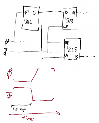
just keep the '573 LE high the entire time PHI2 is low.Initially as PHI2 falls the '573 will start latching "garbage" (whatever was already on the data bus) but it will latch the bank address correctly when it appears. The address is also "garbage" (whatever it was previously) as PHI2 falls but soon correctly appears.
Attachment:
 65C816 BA Latch.png [ 22.08 KiB | Viewed 848 times ]
Then stop the '573 latching by bring LE low as PHI2 rises. This means it takes half a clock cycle to latch the bank address. VDA and VPA are completely separate concerns and have nothing to do with correctly latching the bank address; they indicate what is in the address the '816 is fetching (opcode, program, data or nothing). VDA and VPA and the bank address will change once per clock cycle during an instruction. Although sometimes VDA, VPA and BA will change to the same value they already had.
To get a nice clean PHI2 and /PHI2 run your clock at twice the frequency through a D-Type flip flop and use Q and /Q as PHI2 and /PHI2. That will give you a perfect instantaneous inverse for PHI2. If you don't want to double your clock frequency then you could run your clock into a buffer to get PHI2 and into an inverter to get /PHI2. That will still give you a better inverse than just using an inverter on it's own but depending on your timing characteristics it might not be important.
tokafondo wrote:
Do a latch need a complete clock cycle to do its job?
The latch only needs a half clock cycle to latch. Its output should always be enabled so it is outputting 'something' the entire cycle.
tokafondo wrote:
that would mean that when the CPU goes low, the latch already has the address bank there so a direct memory access could be done.
If by 'CPU goes low' you mean when PHI2 goes high in the second half of the cycle then, yes, at that point the memory access can be done as the latch contains the bank address.
You control when PHI2 goes high and you can think of that as signalling to the '816 that you've latched the bank address and would like it to start writing (or reading) data on the D pins. The bank address and address are output
long before you bring PHI2 high unless you're running at silly high frequencies.


