6502.org Forum  Projects  Code  Documents  Tools  Forum
It is currently Tue Apr 23, 2024 11:57 pm

All times are UTC


Post new topic Reply to topic  [ 13 posts ] 
Author Message
PostPosted: Sat Mar 11, 2023 11:19 am 
Offline
User avatar

Joined: Sun Dec 27, 2020 11:12 pm
Posts: 94
Location: France
Hi everyone,
I was not sure whether to post this here or in Programming, but here goes.
I am trying ( and so far failing) to reliably read data from a CF card.

I built a circuit which seems to work, but I am getting some missed bytes, or sometimes added bytes.

Here is a schematic of the circuit, but note I am using a CF to IDE adapter on my prototype board (to my understanding they are just passive adapters, am I wrong?)

Attachment:
cf-card.png
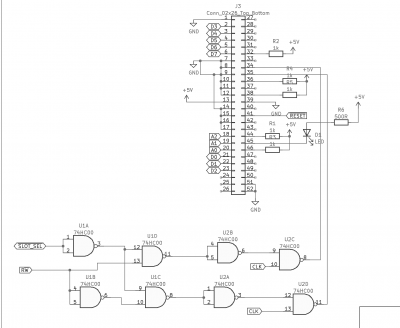
cf-card.png [ 14.88 KiB | Viewed 1026 times ]


Finally, here is the code snippet I use to read a sector from the card (adapted from this code)

Code:
cf_wait:
wait_loop:
    lda CF_ADDRESS + 7
    and #$80
    bne wait_loop
    rts
cf_read:
    phy
    lda #<FAT_BUFFER
    sta CF_BUF_PTR
    lda #>FAT_BUFFER
    sta CF_BUF_PTR + 1
    ldy #0
loop:
    jsr cf_wait
    lda CF_ADDRESS + 7
    and #$08
    beq exit
    lda CF_ADDRESS
    sta (CF_BUF_PTR), y
    iny
    bne loop
    inc CF_BUF_PTR + 1
    bra loop
exit:
    ply
    rts


where FAT_BUFFER is a 512 byte buffer, CF_BUF_PTR is a ZP pointer and CF_ADDRESS is the base address of the CF card.

There is some more code which sets the LBA sector to read, please ask if seeing would be helpful.

And finally here is an example of what I am reading
Code:
EB 3C 90 42 53 44 20 20 34 2E 34 00 02 08 01 00 02 00 02 00 00 F8 F5 00 20 00 20 00 3F 00 00 00
A5 A7 07 00 80 00 29 EB 1A 4C 02 50 4C 41 4E 43 4B 36 35 30 32 20 46 41 54 31 36 20 20 20 FA 31
C0 8E D0 BC 00 7C 8E FB 8E D8 E8 00 00 5E 83 C6 19 BB 07 00 FC AC 84 C0 74 06 B4 0E CD 10 EB F5
30 E4 CD 16 CD 19 0D 0A 4E 6F 6E 2D 73 79 73 74 65 6D 20 64 69 73 6B 0D 0A 50 72 65 73 73 20 61
6E 79 20 6B 65 79 20 74 6F 20 72 65 62 6F 6F 74 0D 0A 00 00 00 00 00 00 00 00 00 00 00 00 00 00
00 00 00 00 00 00 00 00 00 00 00 00 00 00 00 00 00 00 00 00 00 00 00 00 00 00 00 00 00 00 00 00
00 00 00 00 00 00 00 00 00 00 00 00 00 00 00 00 00 00 00 00 00 00 00 00 00 00 00 00 00 00 00 00
00 00 00 00 00 00 00 00 00 00 00 00 00 00 00 00 00 00 00 00 00 00 00 00 00 00 00 00 00 00 00 00
00 00 00 00 00 00 00 00 00 00 00 00 00 00 00 00 00 00 00 00 00 00 00 00 00 00 00 00 00 00 00 00
00 00 00 00 00 00 00 00 00 00 00 00 00 00 00 00 00 00 00 00 00 00 00 00 00 00 00 00 00 00 00 00
00 00 00 00 00 00 00 00 00 00 00 00 00 00 00 00 00 00 00 00 00 00 00 00 00 00 00 00 00 00 00 00
00 00 00 00 00 00 00 00 00 00 00 00 00 00 00 00 00 00 00 00 00 00 00 00 00 00 00 00 00 00 00 00
00 00 00 00 00 00 00 00 00 00 00 00 00 00 00 00 00 00 00 00 00 00 00 00 00 00 00 00 00 00 00 00
00 00 00 00 00 00 00 00 00 00 00 00 00 00 00 00 00 00 00 00 00 00 00 00 00 00 00 00 00 00 00 00
00 00 00 00 00 00 00 00 00 00 00 00 00 00 00 00 00 00 00 00 00 00 00 00 00 00 00 00 00 00 00 00
00 00 00 00 00 00 00 00 00 00 00 00 00 00 00 00 00 00 00 00 00 00 00 00 00 00 00 00 00 00 00 00

And what I should be reading
Code:
EB 3C 90 42 53 44 20 20 34 2E 34 00 02 08 01 00 02 00 02 00 00 F8 F5 00 20 00 20 00 3F 00 00 00
A5 A7 07 00 80 00 29 EB 1A 4C 02 50 4C 41 4E 43 4B 36 35 30 32 20 46 41 54 31 36 20 20 20 FA 31
C0 8E D0 BC 00 7C FB 8E D8 E8 00 00 5E 83 C6 19 BB 07 00 FC AC 84 C0 74 06 B4 0E CD 10 EB F5 30
E4 CD 16 CD 19 0D 0A 4E 6F 6E 2D 73 79 73 74 65 6D 20 64 69 73 6B 0D 0A 50 72 65 73 73 20 61 6E
79 20 6B 65 79 20 74 6F 20 72 65 62 6F 6F 74 0D 0A 00 00 00 00 00 00 00 00 00 00 00 00 00 00 00
00 00 00 00 00 00 00 00 00 00 00 00 00 00 00 00 00 00 00 00 00 00 00 00 00 00 00 00 00 00 00 00
00 00 00 00 00 00 00 00 00 00 00 00 00 00 00 00 00 00 00 00 00 00 00 00 00 00 00 00 00 00 00 00
00 00 00 00 00 00 00 00 00 00 00 00 00 00 00 00 00 00 00 00 00 00 00 00 00 00 00 00 00 00 00 00
00 00 00 00 00 00 00 00 00 00 00 00 00 00 00 00 00 00 00 00 00 00 00 00 00 00 00 00 00 00 00 00
00 00 00 00 00 00 00 00 00 00 00 00 00 00 00 00 00 00 00 00 00 00 00 00 00 00 00 00 00 00 00 00
00 00 00 00 00 00 00 00 00 00 00 00 00 00 00 00 00 00 00 00 00 00 00 00 00 00 00 00 00 00 00 00
00 00 00 00 00 00 00 00 00 00 00 00 00 00 00 00 00 00 00 00 00 00 00 00 00 00 00 00 00 00 00 00
00 00 00 00 00 00 00 00 00 00 00 00 00 00 00 00 00 00 00 00 00 00 00 00 00 00 00 00 00 00 00 00
00 00 00 00 00 00 00 00 00 00 00 00 00 00 00 00 00 00 00 00 00 00 00 00 00 00 00 00 00 00 00 00
00 00 00 00 00 00 00 00 00 00 00 00 00 00 00 00 00 00 00 00 00 00 00 00 00 00 00 00 00 00 00 00
00 00 00 00 00 00 00 00 00 00 00 00 00 00 00 00 00 00 00 00 00 00 00 00 00 00 00 00 00 00 55 AA


As you can see, on line 3 for example I am reading
Code:
8E FB 8E
instead of
Code:
FB 8E


Can anybody see where I am going wrong? The card works perfectly when plugged in my laptop.

Thank you very much for any advice!

Edited to add:
My code seems to work fine, because I can reliably read the card information with ATA command $EC.
I does not seem to be a timing issue either because I get the same types of errors whether I run the computer at 1, 6 or 12 MHz...

_________________
Jonathan Foucher

Take a look at the Planck 6502 computer.


Top
 Profile  
Reply with quote  
PostPosted: Sat Mar 11, 2023 1:16 pm 
Offline
User avatar

Joined: Tue Mar 05, 2013 4:31 am
Posts: 1373
I think you might be having an issue with your hardware setup. The schematic is a bit confusing... as you show a 52-pin connector and compact flash is a 50-pin connector. You noted you're using an adapter, but all of the ones I've used over the years are setup for either a 40-pin IDE interface (with separate power connector) or a 44-pin 2.5-inch IDE connector (integrated power). In any case, these are basically passive, but would have the correct wiring to put the CF Card into IDE mode. Also note that there are two power pins on the CF Card: pins 13 and 38. You have pin 13 to +5V and pin 38 via a 1K resistor to +5V. You also have the /CS0 select tied low and are using a bunch of gates decoding the read and write lines to the CF Card. This might create some timing problems, but maybe not. You show pin 50 as floating, but the SanDisk specification shows pin 50 as Ground.

Attached is the schematic for my compact flash adapter. It's different as I'm also using an 8-bit latch for the upper 8-bits to provide 16-bit data transfers, but the full wiring of the CF Card socket is show with signals grounded, pull-up resistors and such. It might be helpful... but maybe not.

Attachment:
65C02_Pocket_IDE_CF_1.01.png
65C02_Pocket_IDE_CF_1.01.png [ 228.2 KiB | Viewed 1006 times ]


My decode logic is via the ATF16V8 PLD. Note that the chip selects are done via address lines only and not qualified by any clock signals. I also have CLK2 qualified read and write signals that are driving the CF Card read and write lines.

As for the software, you're using 8-bit data mode, so that has to be set first as the default is for 16-bit transfers, which you're probably already doing. My BIOS code (github page) sets up the CF Card and uses interrupt driven transfers. It might be helpful to take a look at it.

Also, Bill (Plasmo on the forum) has a compact flash setup he uses in 8-bit polled mode, so his looking at his CRC65 hardware and software might be helpful as well.

_________________
Regards, KM
https://github.com/floobydust


Top
 Profile  
Reply with quote  
PostPosted: Sat Mar 11, 2023 1:24 pm 
Offline
User avatar

Joined: Fri Dec 11, 2009 3:50 pm
Posts: 3346
Location: Ontario, Canada
Quote:
Here is a schematic of the circuit
Hmm, I'm forced to guess some details. Is CLK the same as PHI2? And is SLOT_SEL the output of an address decoder?

Quote:
I does not seem to be a timing issue either because I get the same types of errors whether I run the computer at 1, 6 or 12 MHz...
Altering the clock speed isn't 100% proof you DON'T have a timing issue. But if CLK is indeed PHI2 then your circuit looks reasonably good to me. You could try replacing the 'HC00 with 'AHC00...

And, is there a transcription error? See below. It looks to me as if the code is calling itself! But I'm still on my first cup of coffee of the day... :) :roll:

-- Jeff


Attachments:
code.jpg
code.jpg [ 38.32 KiB | Viewed 1005 times ]

_________________
In 1988 my 65C02 got six new registers and 44 new full-speed instructions!
https://laughtonelectronics.com/Arcana/ ... mmary.html
Top
 Profile  
Reply with quote  
PostPosted: Sat Mar 11, 2023 2:25 pm 
Offline

Joined: Fri Dec 21, 2018 1:05 am
Posts: 1076
Location: Albuquerque NM USA
A picture is helpful. CF interface is as much as about electrical interface as physical interface. How you physically manage power/ground and fast switching parallel data bus are important. Modern CF is dangerously fast and a great noise maker. High speed is not your friend.
* you should have 3 controls: chip select, read strobe and write strobe. Timing wise, read strobe or write strobe need to be asserted last and negated first. Think of chip select as one of the addresses.
* CF operates at 16-bit data mode natively. There is a "set feature" command to switch it to 8-bit data mode. You should do 8-bit mode to reduce switching noise
* If you found that more '1' you have in your data stream, the more likely it became corrupted, then it is a sure indication of system noise problem. If you lower the voltage (CF is designed to run to 3.3V) and thing starts to work better, it is also an indication of system noise.
* keep it short, keep it simple. I generally don't worry about signal integrity with retro computing but I do with the CF interface.
Bill


Top
 Profile  
Reply with quote  
PostPosted: Sat Mar 11, 2023 5:15 pm 
Offline
User avatar

Joined: Sun Dec 27, 2020 11:12 pm
Posts: 94
Location: France
Hi, and thanks for the quick responses.

I'll try and clarify some things that were not very clear in my first post:

Pins 51 and 52 are the little tabs that hold the connector down on the board. This is the footprint I am using
Attachment:
Capture d’écran 2023-03-11 à 17.53.49.png
Capture d’écran 2023-03-11 à 17.53.49.png [ 57.03 KiB | Viewed 978 times ]


The schematic is not the exact circuit I am using at the moment. It's a design for a board I am planning to make once I have this prototype working. I can see now that it is wrong in a few places. I can draw and post the prototype's schematic if that would be helpful. I used the same decode logic, but I have CE1 (pin 37 on the CF card) tied to the chip select out of the memory decoding. CE0 (pin 38) is tied to ground. Thank you floobydust for your keen eye, I'll make sure to fix these mistakes on the schematic before having the board fabricated. Your schematic will definitely be helpful. Could you also maybe point me to your PLD code so that I could check my own logic against yours ?

Dr Jefyll wrote:
Hmm, I'm forced to guess some details. Is CLK the same as PHI2? And is SLOT_SEL the output of an address decoder?

Yes to both
Dr Jefyll wrote:
It looks to me as if the code is calling itself!

There is an "rts" on the line above "cf_read" that maybe escaped your coffee deprived brain :D
plasmo wrote:
you should have 3 controls: chip select, read strobe and write strobe. Timing wise, read strobe or write strobe need to be asserted last and negated first. Think of chip select as one of the addresses.

Chip select is tied directly to the output of the address decoding.
The read and write strobes are mostly the same, but incorporating the RW signal gated and by the PHI2. Is that enough?
plasmo wrote:
CF operates at 16-bit data mode natively. There is a "set feature" command to switch it to 8-bit data mode. You should do 8-bit mode to reduce switching noise

Yes I am using 8 bit mode (or so I think) by calling this routine before any CF card operation:

Code:
cf_init:
    lda #$4
    sta CF_ADDRESS + 7
    jsr cf_wait
    lda #$E0
    sta CF_ADDRESS + 6
    lda #$1
    sta CF_ADDRESS + 1
    lda #$EF
    sta CF_ADDRESS + 7
    jsr cf_wait
    jsr cf_err
    rts

Does that seem right ?
plasmo wrote:
If you lower the voltage (CF is designed to run to 3.3V) and thing starts to work better, it is also an indication of system noise

Very interesting, I'll give that a try right now!

_________________
Jonathan Foucher

Take a look at the Planck 6502 computer.


Top
 Profile  
Reply with quote  
PostPosted: Sat Mar 11, 2023 5:46 pm 
Offline
User avatar

Joined: Tue Mar 05, 2013 4:31 am
Posts: 1373
Here's the SanDISK technical document I referenced when I was working on the CF Card interface:

Attachment:
SanDisk CompactFlash Memory.pdf [8.59 MiB]
Downloaded 37 times


My GitHub page has the PLD code as well:

https://github.com/floobydust/CF-Card-R ... RTC-CFcard

I use the adapter with my C02 Pocket SBC, full details here:

https://github.com/floobydust/C02-Pocket-SBC

I also have an updated DOS/65 that runs on this configuration:

https://github.com/floobydust/DOS-65-V3.03-ROM

There's also a detailed explanation of the 8-bit latch and PLD code on the forum, albeit a slightly modified interface, as I switched to a 35-pin PATA Microdrive:

viewtopic.php?f=4&t=6825#p96395

Hope this helps...

_________________
Regards, KM
https://github.com/floobydust


Top
 Profile  
Reply with quote  
PostPosted: Sat Mar 11, 2023 7:29 pm 
Offline
User avatar

Joined: Sun Dec 27, 2020 11:12 pm
Posts: 94
Location: France
Would you mind clarifying how the /MRD and /MRW signals are generated? They only appear as inputs on the schematic and in the PLD code.

_________________
Jonathan Foucher

Take a look at the Planck 6502 computer.


Top
 Profile  
Reply with quote  
PostPosted: Sat Mar 11, 2023 7:39 pm 
Offline
User avatar

Joined: Tue Mar 05, 2013 4:31 am
Posts: 1373
jfoucher wrote:
Would you mind clarifying how the /MRD and /MRW signals are generated? They only appear as inputs on the schematic and in the PLD code.


Yes, those are CLK2 qualified lines from the C02 Pocket SBC. The C02 Pocket uses an ATF22V10C PLD as a single glue logic device. All I/O selects, RAM, ROM and /MRD /MWR are generated. Inputs are CLK, R/W and Address lines A15 - A5.

Note that I use page $FE for all I/O. There are 5- selects, each at 32-bytes wide. Using the ATF16V8, I can use a single I/O select to decode for the two selects for the CF-Card (IDE mode), the DS15x1 RTC and the latches. My adapter and BIOS also use interrupts, which requires the INT line from the IDE interface to be inverted.

Here's the basic logic on the PLD:

Code:
Name     Glue3 ;
PartNo   01 ;
Date     10/31/2017 ;
Revision 01 ;
Designer KM ;
Company  Analogue Technologies ;
Assembly SBC2 ;
Location  ;
Device   g22v10 ;

/* *************** INPUT PINS *********************/
PIN 1    = CLK                       ; /*                                 */
PIN 2    = A15                       ; /*                                 */
PIN 3    = A14                       ; /*                                 */
PIN 4    = A13                       ; /*                                 */
PIN 5    = A12                       ; /*                                 */
PIN 6    = A11                       ; /*                                 */
PIN 7    = A10                       ; /*                                 */
PIN 8    = A9                        ; /*                                 */
PIN 9    = A8                        ; /*                                 */
PIN 10   = A7                        ; /*                                 */
PIN 11   = A6                        ; /*                                 */
PIN 13   = A5                        ; /*                                 */
PIN 23   = RW                        ; /*                                 */

/* *************** OUTPUT PINS *********************/
PIN 14   = !IO1                      ; /*                                 */
PIN 15   = !IO2                      ; /*                                 */
PIN 16   = !IO3                      ; /*                                 */
PIN 17   = !IO4                      ; /*                                 */
PIN 18   = !IO5                      ; /*                                 */
PIN 19   = !ROM                      ; /*                                 */
PIN 20   = !RAM                      ; /*                                 */
PIN 21   = !MWR                      ; /*                                 */
PIN 22   = !MRD                      ; /*                                 */

/** Declarations and Intermediate Variable Definitions  **/
FIELD ADDRESS = [A15..0];

RAM = ADDRESS:['h'0000..7FFF];
IO1 = ADDRESS:['h'FE00..FE1F];
IO2 = ADDRESS:['h'FE20..FE3F];
IO3 = ADDRESS:['h'FE40..FE5F];
IO4 = ADDRESS:['h'FE60..FE7F];
IO5 = ADDRESS:['h'FE80..FE9F];
ROM = ADDRESS:['h'8000..FDFF]
        # ADDRESS:['h'FEA0..FFFF];
/** Logic Equations **/
MWR = (CLK & !RW);
MRD = (CLK & RW);

_________________
Regards, KM
https://github.com/floobydust


Top
 Profile  
Reply with quote  
PostPosted: Sat Mar 11, 2023 9:14 pm 
Offline
User avatar

Joined: Sun Dec 27, 2020 11:12 pm
Posts: 94
Location: France
Oh ok, that's really helpful thanks. In your design the chip select only depends on the memory decoding, and the CF card read and write lines only depend on the state of PHI2 and RW, whereas I have the same for the CF card chip select, but my IORD and IOWR signals are "gated" by the chip select, which is not necessary at all.

And Plasmo, I tried running on 3.3V, my CF/IDE adapter has a jumper to set 3.3V or 5V, which I set to 3.3V, but it does not work at all. Any call to the CF card address hangs the whole computer... It was worth a shot anyway.

_________________
Jonathan Foucher

Take a look at the Planck 6502 computer.


Top
 Profile  
Reply with quote  
PostPosted: Sun Mar 12, 2023 11:09 am 
Offline
User avatar

Joined: Sun Dec 27, 2020 11:12 pm
Posts: 94
Location: France
So, what I ended up doing was not trying to read a FAT or other filesystem, and instead just use the block storage that Taliforth expects, since this is what I am using on my machine. After a bit a fiddling, it turns out that reading and writing blocks works perfectly fine there. (I also changed the IORD / IOWR logic to be the simpler one that you use in your PLD, Floobydust). That saves one NAND chip.

For now I have just tried reading / writing ascii data, which works fine. I'll have to try and see what happens with binary data. I think what may be happening is that since ascii data is more "regular", signal integrity is less of an issue and that's why it works fine, whereas with binary data, it's more "random" and signal integrity becomes more of an issue. Is that even possible?

Anyway, I'm calling this solved for now, and thanks for the help!

_________________
Jonathan Foucher

Take a look at the Planck 6502 computer.


Top
 Profile  
Reply with quote  
PostPosted: Sun Mar 12, 2023 5:25 pm 
Offline
User avatar

Joined: Sun Dec 27, 2020 11:12 pm
Posts: 94
Location: France
Final (I hope) update. I finally managed to read random binary data on the CF card by changing my reading code to the code below:
Code:
cf_read:
    phy
    ldy #0
@loop:
    lda CF_ADDRESS
    sta (io_buffer_ptr), y
    iny
    bne @loop
    inc io_buffer_ptr + 1
    jsr cf_wait
@loop2:
    lda CF_ADDRESS
    sta (io_buffer_ptr), y
    iny
    bne @loop2
    dec io_buffer_ptr + 1
@loop3:
    jsr cf_wait
    lda CF_ADDRESS + 7
    and #$08
    beq @exit
    lda CF_ADDRESS
    iny
    bne @loop3
@exit:
    ply
    rts

There is only one call to the cf_wait routine (that calls register 7 to see if the card is ready) when changing from one page to the next, and not at every byte like the previous one.

Also, there no more check for the end of the sector while reading bytes, but that has been moved to the end of the routine. It's a few more bytes, and I don't have a clue why it works, but hey, if it proves ok in the long run, I'm happy!

_________________
Jonathan Foucher

Take a look at the Planck 6502 computer.


Top
 Profile  
Reply with quote  
PostPosted: Sun Mar 12, 2023 7:19 pm 
Offline
User avatar

Joined: Tue Mar 05, 2013 4:31 am
Posts: 1373
When reading or writing to the CF card (or any IDE device), the DRQ bit in the status register is what confirms that data is ready to be transferred. In general, it's unlikely any 6502 based system will be able to grab data faster than the device can output it. I use the routine below, which is part of the ISR that handles the IDE interface. While there is the alternate read from the high-byte latch (D8-D15), the code is simple enough:

Code:
;
INTERUPT1                               ;Interrupt 1 (IDE)
                LDA     IDE_ALT_STATUS  ;Get Alternate Status Register (4)
                BMI     REGEXT01        ;If Busy bit active, just exit (2/3)
;
; - Check for Data Request (DRQ), as the Read LBA operation is the main function
;   of the ISR, which will handle the data transfer from the IDE controller to store the
;   data into memory. This ISR will handle single and multiple block transfers.
;
                LDA     IDE_STATUS      ;Get Status (resets IRQ) (4)
                AND     #%00001000      ;Check for DRQ (2)
                BNE     IDE_READ_BLK    ;Branch if active (2/3)
;
; - If no DRQ is sensed, the other possibilities are:
; 1- A LBA Write has occurred and the interrupt was generated after the transfer.
; 2- A Verify operation has occurred and the interrupt was generated after the verify.
; So we check for these two options and branch accordingly.
;
                BBS2    MATCH,IDE_WRIT_BLK      ;If Bit 2 set, Write operation (5,6)
                BBS1    MATCH,IDE_VRFY_BLK      ;If Bit 1 set, Verify operation (5,6)
                BRA     REGEXT01                ;Exit ISR handler (3)
;
IDE_READ_BLK                            ;IDE Read a Block of data
;
;Note: Arrival here means that the DRQ bit in the status register is active.
; This implies that:
;  1- A LBA Block Read is in progress. If so, the data transfer will be handled below.
;     This also handles multiple LBA Reads and manages the pointers and such. It also
;     clears the LBA Read bit in the MATCH Flag when completed.
;
;  2- A LBA Block Write with multilpe blocks is in progress. If so, the actual data
;     transfer is handled via the IDE WRITE Block routine. An interrupt is generated
;     at the end of each LBA transfer, so that is monitored here and the LBA Write bit
;     in the MATCH Flag is cleared when there are no more blocks to transfer.
;
;Also realize that this ISR will be executed every time the DUART generates an interrupt.
; This will happen every 10ms for the Jiffy-Clock timer and for character transmit and receive.
;
                BBR3    MATCH,REGEXT01  ;If Bit 3 clear, IDE Write (5,6)
;
LBA_XFER        LDA     IDE_ALT_STATUS  ;Get Status  (4)
                AND     #%00001000      ;Check for DRQ (2)
                BEQ     IDE_RD_DONE     ;If not active, done, exit (2/3)
;
IDE_RD_RBLK
                LDA     IDE_DATA        ;Read low byte (high byte in latch) (4)
                STA     (BIOS_XFERL)    ;Store low byte (5)
                INC     BIOS_XFERL      ;Increment pointers (5)
                BNE     IDE_RD_BLK1     ; (2/3)
                INC     BIOS_XFERH      ; (5)
IDE_RD_BLK1
                LDA     IDE_16_READ     ;Read high byte from latch (4)
                STA     (BIOS_XFERL)    ;Store high byte (5)
                INC     BIOS_XFERL      ;Increment pointers (5)
                BNE     LBA_XFER        ;Loop back to Xfer, saves 3 clock cycles (2/3)
                INC     BIOS_XFERH      ; (5)
IDE_RD_BLK2
                BRA     LBA_XFER        ;Loop back till no more DRQs (3)
;
IDE_RD_DONE     DEC     BIOS_XFERC      ;Decrement Block Count to transfer (5)
                BNE     IDE_ALL_DONE    ;Branch around Flag Reset until all blocks moved (2/3)
                RMB3    MATCH           ;Clear Read Block flag (5)
;
IDE_ALL_DONE    LDA     IDE_ALT_STATUS  ;Get Alternate Status Register (4)
                STA     IDE_STATUS_RAM  ;Save it to RAM location (3)
REGEXT01        JMP     (VECINSRT0)     ;Exit ISR handler (6)
;
IDE_WRIT_BLK                            ;IDE Write a Block of data
                LDA     BIOS_XFERC      ;Check Block Count to transfer (3)
                BNE     IDE_ALL_DONE    ;Branch to exit if more blocks need to be moved (2/3)
                RMB2    MATCH           ;Clear Write Block flag (5)
                BRA     IDE_ALL_DONE    ;Branch and finish ISR (3)
;
IDE_VRFY_BLK                            ;IDE Verify a Block of data
                RMB1    MATCH           ;Clear Verify Block flag (5)
                BRA     IDE_ALL_DONE    ;Branch and finish ISR (3)
;


Note that I use the alternate status register for transfers.... as this is a clone of the main status register, with the exception that reading it will not reset the interrupt. Also, by using some of the CMOS instructions and addressing modes, you can make the code a bit smaller for the transfer loop and don't need to preserve the Y reg. I know many folks just prefer to use polled mode here, but I still prefer an interrupt-driven support for hardware devices.

In any case, seems like you've sorted out the hardware and have some routines running to make it go, and as always, you can't argue with success.

_________________
Regards, KM
https://github.com/floobydust


Top
 Profile  
Reply with quote  
PostPosted: Mon Mar 27, 2023 8:17 pm 
Offline
User avatar

Joined: Sun Dec 27, 2020 11:12 pm
Posts: 94
Location: France
Thank you floobydust for the code listing. it helped me a great deal when trying different things. I still had some trouble getting reliable reads from the CF card, even after trying probably everything that was offered here.
I then realized that plasmo's comment about signal integrity was probably on the money, so I had a board fabricated according to the schematic I posted in my first post, modified to take into account everyone's remarks.

Here is the current version.

Attachment:
Capture d’écran 2023-03-27 à 22.11.24.png
Capture d’écran 2023-03-27 à 22.11.24.png [ 416.52 KiB | Viewed 759 times ]


And it turns out that when on a proper PCB, this design works flawlessly! I had a bit of trouble soldering the socket, but apart from that I am very happy with it. I can now use the Taliforth block read and write facilities, and have even played with a very small boot rom (about 200 bytes) that only copies the code from CF to RAM and jumps to it, it's great!

So again, thank you everyone for your help!!

_________________
Jonathan Foucher

Take a look at the Planck 6502 computer.


Top
 Profile  
Reply with quote  
Display posts from previous:  Sort by  
Post new topic Reply to topic  [ 13 posts ] 

All times are UTC


Who is online

Users browsing this forum: No registered users and 12 guests


You cannot post new topics in this forum
You cannot reply to topics in this forum
You cannot edit your posts in this forum
You cannot delete your posts in this forum
You cannot post attachments in this forum

Search for:
Jump to: