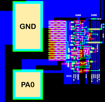
6502.org Forum  Projects  Code  Documents  Tools  Forum
It is currently Sat Apr 27, 2024 9:40 pm

All times are UTC


Post new topic Reply to topic  [ 50 posts ]  Go to page 1, 2, 3, 4  Next
Author Message
 Post subject: 8521 dissection
PostPosted: Wed Nov 30, 2022 10:03 am 
Offline
User avatar

Joined: Fri Nov 09, 2012 5:54 pm
Posts: 1392
Previous thread: 8520 dissection
//In some parts, 8520 and 8521 are pretty similar. In some other parts, they are not...

First: thanks to all those who make these chip dissections possible.

This thread is about a transistor level dissection of the MOS 8521 CIA (Complex Interface Adapter),
brought to you by Frank Wolf and ttlworks.

8521 features two 8 Bit parallel I\O ports (with handshake),
two 16 Bit timers (down counters),
a BCD real time clock (TOD, time of day) with ALARM function,
plus an 8 Bit shift register for "serial communication".

8521 is the HMOS-II successor of the 6526.
8521 is supposed to be a compatible plug_in replacement for the 6526.
8521 was used in: C64, SX64, C128(D), 1570, 1571.

Nevertheless, somebody better check for little differences between 6526, 6526A, 8521.
For instance, whether the ICR (interrupt control register) responds to an interrupt event\source
with a 1 cycle PHI2 delay or not...

Me and Frank were unable to find an 8521 datasheet in the internet.
So I'm linking to the 6526 datasheet intead.

Note:
For consistence with Frank's notation, low_active signals are named foo#, not /foo.

Orientation for all the chip pictures: D2 pad is North.

;---

8521\6526 internally are completely different from the 6522,
and to me it feels like the MOS designers simply had re_invented the wheel
after Bill Mensch (TM) had left MOS.

To make it short: the only thing the 8521 has in common with the 6522 is DIP40.

;===

Now for the difference between 8520 and 8521.

8520:
2) R/W# falling edge is delayed by an inverting super buffer plus three inverters.
4a) PA0..7 have push/pull outputs with a pullup to VCC.
4c) PB6 and PB7 have "open collector" outputs with a pullup to VCC.
5a) FLAG# pad has a pullup to VCC.
5b) TOD pad has a pullup to VCC.
5c) PC# output is "open collector" with pullup to VCC.
7a) CRA7 is cleared on reset, writing to CRA7 has no effect, CRA7 is unused.
8e) in one_shot mode, writing TA_HI sets CRA0 for starting timer A.
9e) in one_shot mode, writing TB_HI sets CRB0 for starting timer B.
10) interrupt source is delayed by one PHI2 cycle before it enters ICR0..4.
14) TOD (time of day) is a 24 Bit binary counter, counting rising edges on the TOD pad without a prescaler.

8521:
2) R/W# falling edge is delayed by four inverters. //slightly less delay than in the 8520.
4a) PA0..7 have "open collector" outputs with a pullup to VCC.
4c) PB6 and PB7 have push/pull outputs with a pullup to VCC.
5a) FLAG# pad has no pullup to VCC.
5b) TOD pad has no pullup to VCC.
5c) PC# is a push/pull output.
7a) CRA7 works and is used for switching the TOD predivider between 50Hz and 60Hz mode.
8e) only a CRA write can set CRA0.
9e) only a CRB write can set CRB0.
10) interrupt source is not delayed by one PHI2 cycle before it enters ICR0..4.
14) TOD (time of day) is a BCD counter, counting rising edges on the TOD pad with a prescaler.

//To make it short: to me, trying to replace a defective 8520 with an 8521 doesn't look like a good idea.

;---
Bugfix:
[Jan 2024] //Maybe dissecting 8520 and 8521 in parallel wasn't a good idea.
Re_calculated resistor values assuming 10kOhm/square FET: 3c, 3c, 4a, 4b, 4c, 5c, 5d, 5e, 13. Done.
A pullup had sneaked into the schematics for SP, CNT: 5d, 5e. Fixed.
PB0..PB5 outputs were not push/pull in the schematics: 4b. Fixed.


Last edited by ttlworks on Mon Jan 08, 2024 3:06 pm, edited 3 times in total.

Top
 Profile  
Reply with quote  
 Post subject: Re: 8521 dissection
PostPosted: Wed Nov 30, 2022 10:03 am 
Offline
User avatar

Joined: Fri Nov 09, 2012 5:54 pm
Posts: 1392
Eagle 6.4 schematics for my schematic pictures in this thread,
just in case if somebody needs them.

Note: KiCad is supposed to be able to import these schematics,
unfortunately it doesn't seem to be possible to disable the layers 'name' and 'value' in KiCad schematics,
so making my schematics look nice and clean in KiCad will require some work, sorry.

Attachment:
8521r1_dissect_schematics.zip [866.35 KiB]
Downloaded 42 times


Last edited by ttlworks on Mon Jan 08, 2024 2:48 pm, edited 1 time in total.

Top
 Profile  
Reply with quote  
 Post subject: Re: 8521 dissection
PostPosted: Wed Nov 30, 2022 10:05 am 
Offline
User avatar

Joined: Fri Nov 09, 2012 5:54 pm
Posts: 1392
A picture of the 8521R1 silicon, with the interesting areas marked.

Attachment:
8521r1_orientation.png
8521r1_orientation.png [ 159.21 KiB | Viewed 2601 times ]


Just as a reference, another picture of the MOS 8521R1 silicon without the markings.

Attachment:
8521r1_small.png
8521r1_small.png [ 928.62 KiB | Viewed 2601 times ]


Last edited by ttlworks on Fri Mar 10, 2023 9:10 am, edited 1 time in total.

Top
 Profile  
Reply with quote  
 Post subject: Re: 8521 dissection
PostPosted: Wed Nov 30, 2022 10:12 am 
Offline
User avatar

Joined: Fri Nov 09, 2012 5:54 pm
Posts: 1392
8521R1 cheat sheet:

Attachment:
8521r1_0_cheatsheet.png
8521r1_0_cheatsheet.png [ 726.83 KiB | Viewed 1828 times ]


Last edited by ttlworks on Mon Jan 08, 2024 2:48 pm, edited 1 time in total.

Top
 Profile  
Reply with quote  
 Post subject: Re: 8521 dissection
PostPosted: Wed Nov 30, 2022 10:13 am 
Offline
User avatar

Joined: Fri Nov 09, 2012 5:54 pm
Posts: 1392
1a) PHI clock generator

Nothing special here.

The external high_active PHI2_in clock signal goes into an inverting super buffer,
which gives out the low_active PHI2_in# clock signal.

PHI2_in# controls a RS flipflop.
The RS flipflop is built from two NOR gates,
the output of every NOR gate is boosted with a non_inverting super buffer,
the super buffers emit the chip internal non_overlapping high_active clock signals PHI1 and PHI2.

Also, PHI2_in# goes into the "2) CS#, R/W#" circuity for generating
the low_active read/write control signals RD# and WE#.

Attachment:
si8521r1_1a_phi_clock_generator.png
si8521r1_1a_phi_clock_generator.png [ 48.13 KiB | Viewed 2600 times ]

Attachment:
8521r1_1a_phi.png
8521r1_1a_phi.png [ 140.09 KiB | Viewed 2600 times ]


Top
 Profile  
Reply with quote  
 Post subject: Re: 8521 dissection
PostPosted: Wed Nov 30, 2022 10:15 am 
Offline
User avatar

Joined: Fri Nov 09, 2012 5:54 pm
Posts: 1392
1b) bias generator

//8521 bias generator is completely different from 8520 bias generator.

Basically we have a ring oscillator, buit from five inverters.
In the signal path of the oscillator, R1\C1..R4\C4 set the frequency.

At the output of the oscillator, we have an inverting and a non_inverting driver.
The output of every driver goes through a big capacitor and into a
bridge rectifier which is built from four FETs working as diodes.

The output of the bidge rectifier then gives us the negative bias voltage.

Attachment:
si8521r1_1b_bias.png
si8521r1_1b_bias.png [ 51.38 KiB | Viewed 2600 times ]

Attachment:
8521r1_1b_bias.png
8521r1_1b_bias.png [ 99.72 KiB | Viewed 2600 times ]


Top
 Profile  
Reply with quote  
 Post subject: Re: 8521 dissection
PostPosted: Wed Nov 30, 2022 10:17 am 
Offline
User avatar

Joined: Fri Nov 09, 2012 5:54 pm
Posts: 1392
2) CS#, R/W# circuitry

It generates the low_active read/write control signals RD# and WE#,
which go into "6) address decoder".

Conceptually, the game is similar to what we had in the 6702 SuperPET dongle chip.

The RD# and WE# signals also go into "3c) D0..D7"
for controlling the buffers/drivers sitting between the external and the internal data bus.

Note, that RD# and WE# also go into "14b) TOD control".

;...

The low_active RD# read control signal comes out of an inverting super buffer,
which is fed by the push/pull output of a three input NOR gate.

At the inputs of the (three input) NOR gate, we have:
PHI2_in# (which is LOW when PHI2_in is HIGH), generated in "1a) PHI clock generator",
The low_active signal from the CS# pad (which indicates that the chip is selected),
The inverted signal from the R/W# pad.

To make it short:
RD# goes active when the chip is selected with CS# = LOW,
and when R/W# = HIGH indicates a read,
and when the system clock PHI2_in = HIGH.

;...

The low_active WE# write control signal comes out of another inverting super buffer,
which is fed by the push/pull output of a four input NOR gate.

At the inputs at the (four input) NOR gate, we have:
PHI2_in# (which is LOW when PHI2_in is HIGH), generated in "1a) PHI clock generator",
The low_active signal from the CS# pad, which indicates that the chip is selected,
The R/W# signal from the R/W# pad,
the R/W# signal from the R/W# pad delayed by four inverters. //slightly less delay than in the 8520.

To make it short:
WE# goes active when the chip is selected with CS# = LOW,
and when R/W# = LOW indicates a write,
and when R/W# was LOW for some time (where "time" is defined by the propagation delays of an inverting super buffer plus three inverters)
and when the system clock PHI2_in = HIGH.

Means the falling edge of R/W# is delayed.
In the C64, the VIC-II uses the bus during PHI2 = LOW, and the CPU uses the bus during PHI2 = HIGH.
Because of this, it takes some time after the rising edge of PHI2 until the R/W# signal generated by the CPU is valid.
I think that's why the designers had added a delay to the 8521 responding to R/W# = LOW writes.

;...

Attachment:
si8521r1_2_cs_rw.png
si8521r1_2_cs_rw.png [ 56.71 KiB | Viewed 2600 times ]

Attachment:
8521r1_2_cs_rw.png
8521r1_2_cs_rw.png [ 170.01 KiB | Viewed 2600 times ]


Top
 Profile  
Reply with quote  
 Post subject: Re: 8521 dissection
PostPosted: Wed Nov 30, 2022 10:20 am 
Offline
User avatar

Joined: Fri Nov 09, 2012 5:54 pm
Posts: 1392
3a) RES#

The low_active signal from the RES# pad goes through an inverting super buffer,
then through a non_inverting super buffer, which emits the high_active RES signal.

RES resets the circuitry on the chip.

Note, that RES# is not synchronized with any clock signal when it becomes RES.

Attachment:
si8521r1_3a_res.png
si8521r1_3a_res.png [ 21.2 KiB | Viewed 2599 times ]

Attachment:
8521r1_3a_res.png
8521r1_3a_res.png [ 30.22 KiB | Viewed 2599 times ]


;---

3b) RS3

RS0..3 pads connect to the external address bus.

Layout for the RS0..3 input buffers is pretty similar, so we just focus on the RS3 circuitry.

Basically, the high_active signal from the RS3 pad goes through an inverting super buffer,
then through two inverters, which control two drivers.

One driver emits the high_active A3 signal,
the other driver emits the low_active A3# signal.

Same thing for RS0..2 becoming A0..A2 and A0#..A2#.

A0..A3 and A0#..A3# go into "6) address decoder" for selecting the register to be read/written.

Attachment:
si8521r1_3b_rs3.png
si8521r1_3b_rs3.png [ 36.04 KiB | Viewed 2599 times ]

Attachment:
8521r1_3b_rs3.png
8521r1_3b_rs3.png [ 44.93 KiB | Viewed 2599 times ]


;---

3c) D0

Layout of the D0..D7 buffers/drivers is pretty identical, so we just focus on D0.

The D0 pad connects to the external data bus.
D0io is the internal databus inside the chip.

To make it simple:
"read" means that the internal D0io..D7io signals are placed on the D0..D7 pads.
"write" means that the signals from the D0..D7 pads are placed on the internal D0io..D7io bus.

;...

At the "write" side, the signal from the D0 pad goes through an inverting super buffer,
is sampled at PHI2 by a transparent latch, and then goes through two more inverters,
and from the inverters into two NOR gates controlling a driver which places the signal on the D0io bus.

The low_active WE# write enable signal which is generated in "2) CS#, R/W# circuitry"
is delayed before it goes into the two NOR gates controlling the driver.

If the low_active write enable signal WE# is LOW, the driver is enabled.

;...

At the "read" side, the signal from the internal D0io bus goes through a non_inverting super buffer,
then through an inverting super buffer and an inverter, controlling two NAND gates
which set/reset a RS flipflop built from two NOR gates which have push/pull outputs.

The outputs of the RS flipflop are controlling the driver FETs which are switching the D0 pad to GND or VCC.
Means that said driver FETs do non_overlapping switching.

Now for the trick:
The low_active RD# read enable signal which is generated in "2) CS#, R/W# circuitry"
goes through an inverter, then into both NAND gates.

So when RD# is HIGH, the outputs of both NANDs are HIGH, forcing both outputs of the RS flipflop to LOW,
what disables the driver FETs which are switching the D0 pad to GND or VCC.

Conceptually, the game is similar to what we had in the 8726 dissection.

;...

Attachment:
si8521r1_3c_d0.png
si8521r1_3c_d0.png [ 70.41 KiB | Viewed 2599 times ]

Attachment:
8521r1_3c_d0.png
8521r1_3c_d0.png [ 72.73 KiB | Viewed 1828 times ]


;---

3d) IRQ#

The low_active IRQout# signal is generated in "10) ICR".

It goes into an inverting super buffer, which drives a FET that switches the IRQ# pad to GND.

Means that when IRQout# is active, the IRQ# pad is switched LOW.

The other end of the IRQ# pad is supposed to be connected to a pullup resistor (to VCC),
and to the IRQ# interrupt input pin of a 65xx CPU.

Attachment:
si8521r1_3d_irq.png
si8521r1_3d_irq.png [ 25.6 KiB | Viewed 2599 times ]

Attachment:
8521r1_3d_irq.png
8521r1_3d_irq.png [ 15.73 KiB | Viewed 1828 times ]


Last edited by ttlworks on Mon Jan 08, 2024 2:51 pm, edited 1 time in total.

Top
 Profile  
Reply with quote  
 Post subject: Re: 8521 dissection
PostPosted: Wed Nov 30, 2022 10:24 am 
Offline
User avatar

Joined: Fri Nov 09, 2012 5:54 pm
Posts: 1392
4a) PA0

Now for the parallel I\O ports, starting with PORT A.

In the silicon, PORT A, PA0..PA7 has push/pull output drivers,
but VCC of the individual drivers ist not connected to VCC of the chip.

So the PORT A output drivers only are able to switching the PA0..PA7 pads to GND.
Means for the "end user", PORT A has "open collector" outputs
with pullup resistors (FETs).

Note, that when a PORT A pin is configured as an output,
what you are getting when reading the PRA data register is
what's on the PA0..PA7 pads.
So you better be a bit paranoid/careful when using read/modify/write instructions
on the PRA register, like when driving a large capacitive load,
when an external source might be able to switch PA0..PA7 to GND,
or when trying to go for faster speed.

Layout for PA0..PA7 is pretty similar, so we just focus on PA0.

Registers and logic related to PA0 are attached to "the other end" of the PA0 pad driver.

PORT A register read/write control signals are generated in "6) address decoder".

;...

At the input side, the signal from the PA0 pad goes through an inverting super buffer,
then through an inverter, is sampled at PHI1 by a dynamic latch, then goes through
another inverter and into an "open collector" NAND gate with its output tied to the D0io bus.

The other input of the NAND is the high active R_PRA register control signal.
R_PRA enables the PRA data register read.

To make it short:
PA0 is sampled by a transparent latch at PHI1.
When the CPU reads the PORTA data register PRA with R_PRA,
if the output of the latch is LOW the D0io bus is pulled LOW.

For pullups on the D0io bus, see "13) internal data bus precharge".

;...

At the output side, first we have the PORTA data direction register Bit DDRA0.

The half_static DDRA0 register Bit is written with the high_active W_DDRA signal at PHI2,
it is refreshed during PHI1, and when RES is active it is cleared at PHI1.

For reading DDRA0 from the CPU:
Basically, the inverted output of the DDRA0 register goes into an
"open collector" NAND gate with its output tied to the D0io bus.

The other input of the NAND is the high active R_DDRA register control signal.
R_DDRA enables the DDRA read at PHI2.

To prevent glitches (during PHI2 register write), the output of the DDRA0 register Bit
is sampled by a transparent latch at PHI1 before it goes into two NAND gates.
The output of each NAND gate goes through an inverter.
The outputs of the inverters are controlling the driver FETs which are switching PA0 to GND (or not to VCC).
When DDRA0 is 0, PA0 acts as an input because said driver FETs are disabled.
When DDRA0 is 1, PA0 acts as an output, and the driver FETs are switching PA0 either to GND (or not to VCC).

//The driver FETs which are supposed to switching to VCC are not connected to VCC, that's why "(or not to VCC)".
//In the 8520, PA0..PA7 drivers are push/pull drivers, switching to VCC indeed.

Also, we have the PRA0 data output register Bit.
The half_static PRA0 register Bit is written with the high_active W_PRA signal at PHI2,
it is refreshed during PHI1, and when RES is active it is cleared at PHI1.

The output of the PRA0 data output register Bit is sampled by a transparent latch at PHI1
to prevent glitches (during PHI2 register writes), then goes through two inverters
which control the two NAND gates, for making the output driver FETs switching PA0
either to GND when data output register Bit PRA0 = 0,
(or not to VCC when data output register Bit PRA0 = 1.)

;...

Attachment:
si8521r1_4a_pa0.png
si8521r1_4a_pa0.png [ 77.16 KiB | Viewed 2598 times ]

Attachment:
8521r1_4a_pa0.png
8521r1_4a_pa0.png [ 102.26 KiB | Viewed 1828 times ]


Last edited by ttlworks on Mon Jan 08, 2024 2:52 pm, edited 1 time in total.

Top
 Profile  
Reply with quote  
 Post subject: Re: 8521 dissection
PostPosted: Wed Nov 30, 2022 10:25 am 
Offline
User avatar

Joined: Fri Nov 09, 2012 5:54 pm
Posts: 1392
4b) PB0

To the "end user", PORT B, PB0..PB5 has push/pull outputs with pullup resistors (FETs).

Note that when a PORT B pin is configured as an output,
what you are getting when reading the PRB data register is
what's on the PB0..PB7 pads.
So you better be a bit paranoid/careful when using read/modify/write instructions
on the PRB register, like when driving a large capacitive load,
when an external source might be able to switch PB0..PB5 to GND,
or when trying to go for faster speed.

Registers and logic related to PB0 are attached "to the other end" of the PB0 pad driver.

PORT B Register read/write control signals are generated in "6) address decoder".

;...

Layout of PB0..PB5 is similar to the layout of PA7
(so I'm not going to explain the same circuitry again here).

Attachment:
si8521r1_4b_pb0.png
si8521r1_4b_pb0.png [ 57.22 KiB | Viewed 2598 times ]

Attachment:
8521r1_4b_pb0.png
8521r1_4b_pb0.png [ 86.45 KiB | Viewed 1828 times ]


Last edited by ttlworks on Mon Jan 08, 2024 2:53 pm, edited 1 time in total.

Top
 Profile  
Reply with quote  
 Post subject: Re: 8521 dissection
PostPosted: Wed Nov 30, 2022 10:26 am 
Offline
User avatar

Joined: Fri Nov 09, 2012 5:54 pm
Posts: 1392
4c) PB7

PB7 (and PB6) circuitry builds on the PB0..PB5 circuitry.

Except that the FETs of the output drivers switching to VCC really are connected to VCC,
means that PB7 (and PB6) have push/pull outputs with a pullup FET to VCC.

The difference to PB0..PB5 is, that if the CRB1 Bit in control register B is set,
PB7 is forced to work as an output (ignoring DDRB7) and is assigned to timer B,
emitting either a pulse or a toggle signal at timer B underflow.

For PB6, it's the CRA1 Bit in control register A, and timer A.

;---

Now for what's different in PB7 when comparing it with PB0:

A multiplexer controlled by CRB1 switches either the output of the
PRB7 data output register to the PB7 output driver circuitry,
or the high_active signal TB_Q which is generated in "9e) timer B control logic".
//For PB6, TA_Q is generated in "8e) timer A control logic".

To prevent glitches (during PHI2 register writes), the inverted output of the
DDRB7 data direction register Bit is sampled by a transparent latch at PHI1,
and goes into a NAND gate together with the CRB1 signal.
If the output of the NAND gate is LOW, the PB7 output driver is disabled.

In other words: if DDRB7 = 1, or CRB1 = 1, the PB7 pad output driver is enabled.
//and again: PB6 and PB7 are the only PORT pads which have push/pull drivers.

Attachment:
si8521r1_4c_pb7.png
si8521r1_4c_pb7.png [ 65.23 KiB | Viewed 2598 times ]

Attachment:
8521r1_4c_pb7.png
8521r1_4c_pb7.png [ 106.9 KiB | Viewed 1828 times ]


Last edited by ttlworks on Mon Jan 08, 2024 2:54 pm, edited 1 time in total.

Top
 Profile  
Reply with quote  
 Post subject: Re: 8521 dissection
PostPosted: Wed Nov 30, 2022 10:27 am 
Offline
User avatar

Joined: Fri Nov 09, 2012 5:54 pm
Posts: 1392
5a) FLAG# pad

A falling edge at the FLAG# pad sets the FLAG Bit in the ICR. //Interrupt control register.
FLAG# is a handshake input related to the parallel I\O ports.

Note, that there is no pullup resistor (FET) on the chip which ties the FLAG# pad to VCC.
//in the 8520, there _is_ a pullup FET to VCC.

;...

The signal from the FLAG# pad goes through an inverting Schmitt trigger,
then through an inverter, an inverting super buffer, and another inverter, into a falling edge detector.

At the output of the falling edge detector, we have a NOR gate.
One input of the NOR gate directly is fed with the edge detector input signal,
the other input of the NOR is fed with the delayed/inverted edge detector input signal.
So when a falling edge is detected, the NOR gate emits a HIGH pulse
(the width of the pulse is set by the delay).

The inversion/delay is done by four "open collector" inverters which have a pullup
to VCC and a capacitor to GND at their outputs, plus a normal inverter.


We have the first RS flipflop which indicates that there was a falling edge on the FLAG# pad,
it is set by the output of the detector NOR,
and cleared by the FLAG_INT signal (which sets the FLAG Bit in the ICR).

The output of the first flipflop goes into a multifunction gate,
which basically is a second RS flipflop gated with PHI2.
The (inverted) output of the second RS flipflop is sampled at PH1 by a dynamic latch,
goes through an inverter, and becomes the FLAG_INT signal,
which now nicely is synchronized with the system clock.

Signal FLAG_INT goes into "10) ICR".

//Funny thing is: when I had tried building a TTL implementation of the 6522, I independently came up with the same concept.

Attachment:
si8521r1_5a_flag.png
si8521r1_5a_flag.png [ 60.02 KiB | Viewed 2598 times ]

Attachment:
8521r1_5a_flag.png
8521r1_5a_flag.png [ 200.76 KiB | Viewed 2598 times ]


Top
 Profile  
Reply with quote  
 Post subject: Re: 8521 dissection
PostPosted: Wed Nov 30, 2022 10:29 am 
Offline
User avatar

Joined: Fri Nov 09, 2012 5:54 pm
Posts: 1392
5b) TOD pad

Short form:

TOD pad is supposed to be fed with a signal generated by AC mains frequency.
A predivider is used for dividing the TOD pad input frequency down to 10Hz.
TOD (time of day) real time clock is a BCD counter,
to get a correct time said BCD counter has to run at these 10Hz.

In some countries AC mains frequency is 50 Hz,
then you need to write '1' into CRA7, to make the predivider divide by 5.

in some other counties AC mains frequency is 60Hz,
then you need to write '0' into CRA7, to make the predivider divide by 6.

Note, that there is no pullup resistor (FET) to VCC at the TOD pad.
//in the 8521, there is a pullup.

;...

Long form:

Close to the TOD pad we have a ring counter which generates the PHI20 clock
for the TOD pad edge detector\synchronizer, for the predivider, and for the TOD counter.

I had labeled that clock signal "PHI20", because it is HIGH at PHI2 in every fourth PHI2 clock cycle.

Means that the TOD counter is clocked with PHI2/4, and enabled with a rising edge at the TOD pad.


When designing the circuity which extracts the frequency from AC mains and sends it into the TOD pad:
8521 has no pullup at the TOD pad. //8520 has a pullup at the TOD pad.


The TOD edge detector and synchronizer circuitry builds on the FLAG# edge detector and synchronizer circuitry,
but there are some differences:

There is one less inverter between the TOD pad and the edge detector,
so we have a falling edge detector scanning the inverted signal from the TOD pad.
//And that's like having a rising edge detector scanning the non_inverted signal from the TOD pad.

The multifunction gate containing the second RS flipflop is gated with PHI20 (instead of PHI2),
for sampling the state of the first RS flipflop,
to synchronize the output signal with the TOD counter clock PHI20.

A transparent latch samples the (inverted) output of the second RS flipflop at PHI2,
sends it into a NOR gate together with the RES signal.
The high_active TOD_DET output of the NOR gate resets the first RS flipflop,
aknowledging that the rising edge at the TOD pad was recognized.

Means that if there was a rising edge at the TOD pad while RES is active,
TOD_DET goes active after RES goes inactive.


TOD_DET is sampled by a PHI20 controlled latch, then goes into the predivider.
To be more precisely, it becomes the clock for the four dynamic master/slave flipflops
which make up the ring counter that divides by 5 (CRA7=1) or 6 (CRA7=0).

The output of the predivider counter Bits changes at the TOD_DET falling edge.
Three of the master/slave flipflops are actually counting.
The fourth master/slave flipflop clears the three counter Bits on predivider overflow.

High_active control signal TOD_STOP is generated in "14b) TOD control".
After a write to TOD_10THS, TOD_STOP goes active and prevents the TOD BCD counter from counting
by forcing the fourth master/slave flipflop of the predivider to clear the predivider counter Bits.

For cycle correct timing on how the master/slave flipflops respond to TOD_DET, TOD_STOP and overflow,
please go down the rabbit hole from simplified TTL equivalent schematic to transistor level schematic.


The predivider generates a pulse on TOD_DET1 at overflow.


An edge detector (which is part of "14d) TOD_Cin_T1#" enables TOD BCD counter counting
for one counting step after a rising edge on TOD_DET1.

Attachment:
si8521r1_5b_tod.png
si8521r1_5b_tod.png [ 130.82 KiB | Viewed 2598 times ]

Attachment:
8521r1_5b_tod_pad.png
8521r1_5b_tod_pad.png [ 283.49 KiB | Viewed 2598 times ]


Top
 Profile  
Reply with quote  
 Post subject: Re: 8521 dissection
PostPosted: Wed Nov 30, 2022 10:30 am 
Offline
User avatar

Joined: Fri Nov 09, 2012 5:54 pm
Posts: 1392
5c) PC# pad

PC# is a push/pull handshake output, which generates a LOW pulse in the PHI2 cycle
after a PORT B data register read or write cycle.

//in the 8520, PC# is an "open collector" output with no pullup FET.
//in the 8520, there is a two PHI2 cycles delay between PORT B data register read/write and pulse output.

;...

R_PRA (PRA read enable signal) and W_PRA (PRB write enable signal) go into a NOR gate,
which feeds the inputs of a shift register which is built from transparent latches (controlled by PHI1 and PHI2)
and inverters.

A NOR gate attached to said shift register controlls the driver which switches the PC# pad to GND.

Basically, PC# logic works like an edge detector for 'R_PRA OR W_PRA'.

My guess is that the designers wanted to limit the length of the PC# pulse,
like when it comes to read/modify/write cycles on PRA or PRB,
or when the PRA\PRB read/write is stretched for multiple PHI2 cycles while the CPU is hold by RDY.

Attachment:
si8521r1_5c_pc.png
si8521r1_5c_pc.png [ 47.29 KiB | Viewed 2598 times ]

Attachment:
8521r1_5c_pc.png
8521r1_5c_pc.png [ 56.82 KiB | Viewed 1828 times ]


Last edited by ttlworks on Mon Jan 08, 2024 2:56 pm, edited 1 time in total.

Top
 Profile  
Reply with quote  
 Post subject: Re: 8521 dissection
PostPosted: Wed Nov 30, 2022 10:31 am 
Offline
User avatar

Joined: Fri Nov 09, 2012 5:54 pm
Posts: 1392
5d) SP pad

SP pad is the data input/putput pad for the serial port (shift register).

CRA6 control register A Bit configurates the serial port to either work
as an input (CRA6 = 0) or as an output (CRA6 = 1).

In output mode, SP has an "open collector output".

Note, that there is no pullup resistor (FET) on the chip which ties the SP pad to VCC.

;...

At the input side,
the high_active signal from the SP pad goes through an inverting super buffer,
then through an inverter, then together with CRA6 into a NOR gate,
which emits the low_active serial data input signal SP_RXD#.

In output mode, when CRA6 is HIGH, SP_RXD# is forced to LOW (active).

SP_RXD goes into "11a) shift register plus latch".

;...

At the output side,
the low_active serial data output signal SP_TXD# goes together with CRA6 into a NAND gate.
The output signal of the NAND gate goes into an inverting super buffer,
which controlls the driver FETs switching the SP pad to GND.

When CRA6 is HIGH (serial port in output mode), and SP_TXD# is HIGH (inactive),
the SP pad is switched to GND.

SP_TXD# is generated in "11b) serial port control".

Note, that there is some dead circuitry (maybe from a previous chip revision),
to me it looks like the designer who did the SP pad buffer/driver was not sure
whether he would be getting a high_active or a low_active serial data output signal
from the shift register... and he wanted to be on the safe side.
So we just ignore that part.

;...

Attachment:
si8521r1_5d_sp.png
si8521r1_5d_sp.png [ 37.51 KiB | Viewed 2598 times ]

Attachment:
8521r1_5d_sp.png
8521r1_5d_sp.png [ 38.61 KiB | Viewed 1828 times ]


Last edited by ttlworks on Mon Jan 08, 2024 2:57 pm, edited 1 time in total.

Top
 Profile  
Reply with quote  
Display posts from previous:  Sort by  
Post new topic Reply to topic  [ 50 posts ]  Go to page 1, 2, 3, 4  Next

All times are UTC


Who is online

Users browsing this forum: No registered users and 30 guests


You cannot post new topics in this forum
You cannot reply to topics in this forum
You cannot edit your posts in this forum
You cannot delete your posts in this forum
You cannot post attachments in this forum

Search for:
Jump to: