6502.org Forum  Projects  Code  Documents  Tools  Forum
It is currently Sat Apr 27, 2024 8:05 pm

All times are UTC


Post new topic Reply to topic  [ 50 posts ]  Go to page Previous  1, 2, 3, 4  Next
Author Message
 Post subject: Re: 8521 dissection
PostPosted: Wed Nov 30, 2022 10:32 am 
Offline
User avatar

Joined: Fri Nov 09, 2012 5:54 pm
Posts: 1392
5e) CNT pad

CNT pad is the clock input/putput pad for the serial port (shift register),
also it can be used to enable timer A or timer B counting.

CRA6 control register A Bit configurates the serial port to either work
as an input (CRA6 = 0) or as an output (CRA6 = 1).

In input mode, the serial shift clock has to be generated outside the chip, and sent into the CNT pad.
In output mode, the serial shift clock is generated inside the chip, and comes out of the CNT pad.

In output mode, CNT has an "open collector output".
The output circuitry related to the CNT pad isn't much different from what we had at the SP pad.

Note, that there is no pullup resistor (FET) on the chip which ties the CNT pad to VCC.

;...

At the input side,
the high_active signal from the CNT pad goes through an inverting Schmitt trigger,
an inverter, an inverting super buffer, and becomes the low_active CNT# signal.

CNT# then goes into "12) CNT edge detector", which technically senses a rising edge on the CNT pad,
and generates the high_active CNT_EDGE signal if this was the case.

CNT_EDGE goes into "11b) serial port control", where it is used for generating the clock signal
for "11a) shift register plus latch".

CNT_EDGE also goes into "8c) timer A LO carry input generation".
CNT_EDGE and CNT# also go into "9c) timer B LO carry input generation".

;...

At the output side,
the low_active serial output clock signal SP_TCK# goes together with CRA6 into a NAND gate.
The output of the NAND gate goes into an inverting super buffer,
which controlls the driver FETs switching the CNT pad to GND.

When CRA6 = 1 (serial port in output mode), and SP_TCK# is HIGH (inactive),
the CNT pad is switched to GND.

The SP_TCK# signal is generated in "11b) serial port control".

;...

Attachment:
si8521r1_5e_cnt.png
si8521r1_5e_cnt.png [ 42.26 KiB | Viewed 1621 times ]

Attachment:
8521r1_5e_cnt.png
8521r1_5e_cnt.png [ 33.85 KiB | Viewed 1276 times ]


Last edited by ttlworks on Mon Jan 08, 2024 2:57 pm, edited 1 time in total.

Top
 Profile  
Reply with quote  
 Post subject: Re: 8521 dissection
PostPosted: Wed Nov 30, 2022 10:35 am 
Offline
User avatar

Joined: Fri Nov 09, 2012 5:54 pm
Posts: 1392
6) address decoder

The address decoder generates all of the high_active register read/write control signals.

It is fed with the RD# (read enable) and WE# (write enable) control signals
which are generated in "2) CS#, R/W#".

It also is fed with the high_active address signals A0..A3 and the low_active address_signals A0#..A3#,
which are generated in "3b) RS0..RS3" for selecting the register to be read/written.

Also, the CRB7 control register B Bit goes into the address decoder.
If CRB7 = 0, writes to address $8,$9,$A,$B write the TOD counter registers.
If CRB7 = 1, writes to address $8,$9,$A,$B write the ALARM registers.

Note the high_active select signal SEL_$B,
which becomes active if the address signals say $B,
regardless of RD# and WE#.
It goes into "14b TOD control".

;...

The address decoder is built with NOR gates (plus a few inverters),
it breaks down into individual blocks (for the different registers),
and said blocks are spread all over the chip.

Attachment:
si8521_addressdecoder_orientation.png
si8521_addressdecoder_orientation.png [ 61.09 KiB | Viewed 1621 times ]


In the North half of the chip (6a..6e),
the address decoder blocks generate the read/write register control signals
for timer A, timer B, CRA, CRB, ICR.
Every single control signal is generated by a 5 input NOR gate.
Note the FET which pulls D4io to GND when R_CRA goes active for reading CRA.

In the South half of the chip (6f..6h),
the address decoder blocks generate the read/write register control signals
for the parallel I\O ports, the serial port (shift register),
the TOD counter registers, and the ALARM registers.
In every block, we have a 4 input NOR gate decoding the address,
which feeds an inverter.
The inverter output goes into two NOR gates
(one generating a read control signal, the other generating a write control signal),
for the TOD counter and the ALARM register it's a bit more circuitry because of CRB7.

I think that the designers had used different address decoder circuitry for the
North half and the South half of the chip to make better use of chip space.
BTW: the address decoder blocks in the North have less propagation delay
than the address decoder blocks in the South.

TTL equivalent of the whole address decoder:

Attachment:
8521_6_addressdecoder_part0.png
8521_6_addressdecoder_part0.png [ 154.44 KiB | Viewed 1621 times ]


Top
 Profile  
Reply with quote  
 Post subject: Re: 8521 dissection
PostPosted: Wed Nov 30, 2022 10:47 am 
Offline
User avatar

Joined: Fri Nov 09, 2012 5:54 pm
Posts: 1392
Now for the individual parts that make up the address decoder:

Attachment:
si8521r1_6a_address_decoder.png
si8521r1_6a_address_decoder.png [ 26.85 KiB | Viewed 1619 times ]

Attachment:
8521r1_6a_addressdecoder_part1.png
8521r1_6a_addressdecoder_part1.png [ 54.84 KiB | Viewed 1619 times ]

;...
Attachment:
si8521r1_6b_address_decoder.png
si8521r1_6b_address_decoder.png [ 14.6 KiB | Viewed 1619 times ]

Attachment:
8521r1_6b_addressdecoder_part2.png
8521r1_6b_addressdecoder_part2.png [ 38.6 KiB | Viewed 1619 times ]

;...
Attachment:
si8521r1_6c_address_decoder.png
si8521r1_6c_address_decoder.png [ 25.47 KiB | Viewed 1619 times ]

Attachment:
8521r1_6c_addressdecoder_part3.png
8521r1_6c_addressdecoder_part3.png [ 54.05 KiB | Viewed 1619 times ]

;...
Attachment:
si8521r1_6d_address_decoder.png
si8521r1_6d_address_decoder.png [ 14.7 KiB | Viewed 1619 times ]

Attachment:
8521r1_6d_addressdecoder_part4.png
8521r1_6d_addressdecoder_part4.png [ 39.46 KiB | Viewed 1619 times ]

;...
Attachment:
si8521r1_6e_address_decoder.png
si8521r1_6e_address_decoder.png [ 13.65 KiB | Viewed 1619 times ]

Attachment:
8521r1_6e_addressdecoder_part5.png
8521r1_6e_addressdecoder_part5.png [ 39.23 KiB | Viewed 1619 times ]

;...
Attachment:
si8521r1_6f_address_decoder.png
si8521r1_6f_address_decoder.png [ 59.14 KiB | Viewed 1619 times ]

Attachment:
8521r1_6f_addressdecoder_part6.png
8521r1_6f_addressdecoder_part6.png [ 364.54 KiB | Viewed 1619 times ]

;...
Attachment:
si8521r1_6g_address_decoder.png
si8521r1_6g_address_decoder.png [ 26.78 KiB | Viewed 1619 times ]

Attachment:
8521r1_6g_addressdecoder_part7.png
8521r1_6g_addressdecoder_part7.png [ 51.08 KiB | Viewed 1619 times ]

;...
Attachment:
si8521r1_6h_address_decoder.png
si8521r1_6h_address_decoder.png [ 42.78 KiB | Viewed 1619 times ]

Attachment:
8521r1_6h_addressdecoder_part8.png
8521r1_6h_addressdecoder_part8.png [ 183.58 KiB | Viewed 1619 times ]


Top
 Profile  
Reply with quote  
 Post subject: Re: 8521 dissection
PostPosted: Wed Nov 30, 2022 10:49 am 
Offline
User avatar

Joined: Fri Nov 09, 2012 5:54 pm
Posts: 1392
7) CRA, CRB //control register A, control register B

The CRA (control register A) and CRB (control register B) Bits are located
North of timer A and Timer B.

;---

For CRA1..CRA7 and CRB1..CRB7, the layout of the register Bits is pretty similar,
a register Bit cell is just a half_static latch,
written with high_active control signal W_CRA (or W_CRB) at PHI2, refreshed at PHI1,
cleared at PHI1 when RES is active.

Outputs of the register Bits which control circuitry on the chip are sampled
by transparent latches at PHI1 to prevent glitches (during PHI2 register writes).

The register Bits can be read back on the internal data bus,
controlled by high_active read control signal R_CRA (or R_CRB).

//in the 8520, the CRA7 register Bit write enable is permanently disabled.

Attachment:
si8521r1_7a_cra6.png
si8521r1_7a_cra6.png [ 12.15 KiB | Viewed 1619 times ]


;---

CRA0 and CRB0 build on the layout of the other CRA\CRB register Bits,
but there is some additional circuitry related to timer control.
Besides that, the outputs of CRA0 and CRB0 which go into the
timer A and timer B control circuitry are low_active.

CRA0 enables timer A, CRB0 enables timer B.
Layout for CRA0 and CRB0 is identical, so we focus on CRA0.


CRA3=1 indicates, that timer A is running in one_shot mode.

High_active signal TAH_TC indicates that timer A will roll over
from $0000 to $FFFF in the next PHI2 cycle when timer A counting is enabled
(that's timer A underflow).
It is generated in "8b) timer A HI".

When CRA3 and TAH_TC are active,
CRA0 is cleared (at PHI1) to stop timer A counting.

CRB0 and the related timer B circuitry are pretty much identical to this.


//in the 8521, writing TA_HI when timer A is in one_shot mode sets CRA0.
//in the 8521, writing TB_HI when timer B is in one_shot mode sets CRB0.

Attachment:
si8521r1_7a_cra0.png
si8521r1_7a_cra0.png [ 14.36 KiB | Viewed 1619 times ]


;---

Attachment:
8521r1_7_cra_crb.png
8521r1_7_cra_crb.png [ 178.94 KiB | Viewed 1619 times ]


Top
 Profile  
Reply with quote  
 Post subject: Re: 8521 dissection
PostPosted: Wed Nov 30, 2022 10:51 am 
Offline
User avatar

Joined: Fri Nov 09, 2012 5:54 pm
Posts: 1392
8a) timer A LO //Bit 0..7

Timer A LO is a block of 8 cells, one Bit per cell, it's the timer A low Byte.

;...

North half of the cells are the timer A registers,
which are written by the CPU.

Registers are half_statich latches, and they are
written by high_active control signal W_TA_LO at PHI2,
refreshed at PHI1, and cleared with RES at PHI1.

The basic concept isn't different from what we had
in the CRA\CRB control registers.

Also, the CPU can read the contents of the counter cells
with the high_active control signal R_TA_LO.

;...

South half of the cells are the timer A counter Bits,
and it's a down counter.

The CPU only can write the registers,
the registers are transferred into the counter cells
by the high_active control signal TA_LD which changes at PHI1,
it is generated in "8e) timer control logic".

Counter cells use an inverting/non inverting ripple carry,
the low_active carry input of the LSB is at the West side of the 8 Bit block.

Also, the counter cells store the Bits in non_inverted/inverted form.

The result for the next counting step is latched at PHI2,
and transferred into the counter Bits with high_active control signal TA_CNT
at PHI1.

TAL_TC basically is a NOR gate, which checks for 8 Bit counter underflow.
It changes at PHI2, and it becomes HIGH when the 8 Bit counter is $00
with "the count enabled".
//For "count enabled", see "8c) timer A LO input carry generation.

Two timer A LO cells look like this:

Attachment:
si8521r1_8a_timer_a_lo.png
si8521r1_8a_timer_a_lo.png [ 42.72 KiB | Viewed 1619 times ]

Attachment:
8521r1_8a_ta_lo.png
8521r1_8a_ta_lo.png [ 200.02 KiB | Viewed 1619 times ]


;---

8b) timer A HI //Bit 8..15

Timer A HI is a block of 8 cells, it's the timer A high Byte.

The layout is identical to "8a) timer A LO".

For "count enabled", see "8d) timer A HI input carry generation".


Top
 Profile  
Reply with quote  
 Post subject: Re: 8521 dissection
PostPosted: Wed Nov 30, 2022 10:53 am 
Offline
User avatar

Joined: Fri Nov 09, 2012 5:54 pm
Posts: 1392
8c) timer A LO input carry generation

It generates the low_active input carry for the timer A LO Bit 0,
means it enables/disables timer A down counting.

In the silicon, it is located West from timer A LO.

;...

The high_active signal CNT_EDGE is generated in "12) CNT edge detector",
it is active for one PHI2 cycle after there was a rising edge on the CNT pad.

When CRA5 = 0, counting always would be enabled, and timer A LO decrements at PHI2 speed.
When CRA5 = 1, counting would be enabled for one step after there was a rising edge on the CNT pad.

An inverter plus a NAND gate check if that is the case.
The output of the NAND gate is sampled by a transparent latch at PHI2.

The output of the transparent latch goes into a NAND gate,
together with the high_active control signal TA_CEN
which is generated in "8a) timer control logic" from CRA0.

//CRA0 in control register A enables/disables timer A counting in general.

If the output of that NAND gate is low (active),
the NOR gate TAL_TC is enabled for sensing timer A LO underflow.
Also, for counting one step the low_active carry input of the timer A LO Bit 0
goes active... when the high_active control signal TA_LD does not load the
timer A counter from the timer A registers.

//Note, that TA_LD changes at PHI1.

Attachment:
si8521r1_8c_ta_cin0.png
si8521r1_8c_ta_cin0.png [ 20.69 KiB | Viewed 1619 times ]

Attachment:
8521r1_8c_ta_lo_cin.png
8521r1_8c_ta_lo_cin.png [ 54.12 KiB | Viewed 1619 times ]


;---

8d) timer A HI input carry generation

It generates the low_active input carry for timer A HI.

In the silicon, it is located between timer A LO and timer A HI.

;...

If timer A LO counting is enabled, and if timer A LO is $00,
the high_active signal TAL_TC becomes HIGH for indicating a timer A LO underflow.

If TAL_TC is high, the NOR gate TAH_TC which checks for timer A HI underflow is enabled.
Also, the low_active input carry for the timer A HI Bit 8 goes active...
when the high_active control signal TA_LD does not load the
timer A counter from the timer A registers.

Because of this, TAH_TC actually indicates an underflow for the whole
16 Bit timer A if counting is enabled.

//Note, that TA_LD changes at PHI1.

Attachment:
si8521r1_8d_ta_cin8.png
si8521r1_8d_ta_cin8.png [ 9.82 KiB | Viewed 1619 times ]

Attachment:
8521r1_8d_ta_hi_cin.png
8521r1_8d_ta_hi_cin.png [ 26.83 KiB | Viewed 1619 times ]


Top
 Profile  
Reply with quote  
 Post subject: Re: 8521 dissection
PostPosted: Wed Nov 30, 2022 10:55 am 
Offline
User avatar

Joined: Fri Nov 09, 2012 5:54 pm
Posts: 1392
8e) timer A control logic

It's quite big, and in the silicon it's located East of timer A HI
and East of the CRA0 control register A register Bit.
//in the 8520, timer A control logic is even bigger.

It controls the timer A counter cells (by signals TA_CNT, TA_LD, TA_CEN),
it generates the timer a underflow interrupt signal (signal TA_INT),
it generates the pulse\toggle output signal TA_Q which goes to the PB6 pad driver,
and it clears CRA0 at timer A underflow when timer A is in one shot mode.

;...

About controlling the timer A counter cells:

High_active control signal TA_CEN enables timer A counting in
"8c) timer A LO input carry generation".
;
TA_CEN is the output of a latch which samples CRA0 at PHI2.
//At PHI2 in the cycle after the CRA register write cycle.

High_active control signal TA_CNT loads the timer A counter cells
with the result of the next counting step at PHI1.
It is active by default at PHI1 when TA_LD is not active at PHI1.

High_active control signal TA_LD transfers the contents
of the timer A registers into the timer A counter cells,
it changes at PHI1.

There are four conditions which enable TA_LD:
;
RES is active.
;
There is a timer A underflow with counting enabled.
;
Load is forced for one PHI2 cycle after writing 1 to CRA4
(by high_active CRA write control signal W_CRA).
;
When timer A was set to continous mode (at least) in the previous cycle,
and when timer A counting was disabled by TA_CEN = LOW,
in the PHI2 cycle after a TA_HI register write.

;...

About TA_Q and timer A underflow interrupt:

High_active signal TAH_TC indicates a timer A underflow when counting is enabled.
TAH_TC is sampled by a transparent latch at PHI1.
The output of the latch gives us the high_active signal TA_INT,
which will set the timer A interrupt flag.

When CRA2 = 0, TA_Q is the inverted TA_INT signal.
TA_Q then changes at PHI1 and goes LOW for one PHI2 cycle.

When CRA2 = 1, TA_Q comes out of what basically is a one Bit counter
built from two AND\NOR gates and two transparent latches.
The counter advances at PHI1 when TA_INT is active.
The counter output which goes into TA_Q is forced to LOW at PHI1
by a rising edge detector in the PHI2 cycle after CRA0 changes from 0 to 1.
Also, the counter output which goes into TA_Q asynchronously is forced
to HIGH when RES is active.

;...

About timer A control logic clearing CRA0:

If CRA3 = 0, timer A is in continous mode.
If CRA3 = 1, timer A is in one shot mode.

//in the 8521, there is some additional logic for setting CRA0 after a TA_HI write when timer A is in one shot mode.

Short form:
If there is a timer A underflow while timer A is in one shot mode, CRA0 is cleared.

Now for the longer version:

Output of register Bit CRA3 and high_active signal TAH_TC (which indicates
a timer A underflow with counting enabled go into "7a) CRA0".
If both signals are active, this clears CRA0 at PHI1.

;...

Attachment:
si8521r1_8e_timer_a_control.png
si8521r1_8e_timer_a_control.png [ 67.81 KiB | Viewed 1619 times ]

Attachment:
8521r1_8e_ta_control_logic.png
8521r1_8e_ta_control_logic.png [ 378.47 KiB | Viewed 1619 times ]


Top
 Profile  
Reply with quote  
 Post subject: Re: 8521 dissection
PostPosted: Wed Nov 30, 2022 10:57 am 
Offline
User avatar

Joined: Fri Nov 09, 2012 5:54 pm
Posts: 1392
9a) timer B LO: same layout as "8a) timer A LO".
9b) timer B HI: same layout as "8b) timer 8 HI".
9d) timer B HI input carry generation: same layout as "8d) timer A HI input carry generation".
9e) timer B control logic: same layout as "8e) timer A control logic".

;---

9c) timer B LO input carry generation //different from 8c.

It builds on "8c) timer A LO input carry generation",
but it has some additional circuitry.

Timer B counting would be enabled if:
CRB6=0, CRB5=0: always. //that's counting at PHI2 speed
CRB6=0, CRB5=1: for one step after there was a rising edge on the CNT pad.
CRB6=1, CRB5=0: at timer A underflow with timer A counting enabled. //forming a 32 Bit counter/timer
CRB6=1, CRB5=1: at timer A underflow with timer A counting enabled, and when CNT pad was high in the provious PHI2 cycle.

The rest of the circuitry isn't any different from "8c) timer A LO carry input generation".

Attachment:
si8521r1_9c_tb_cin0.png
si8521r1_9c_tb_cin0.png [ 31.97 KiB | Viewed 1619 times ]

Attachment:
8521r1_9c_tb_lo_cin.png
8521r1_9c_tb_lo_cin.png [ 100.69 KiB | Viewed 1619 times ]


;---

Now for a bigger picture showing the simplified schematic
of timer A, plus timer B, plus the related control logic:

Attachment:
8521r1_8_9_timer_section.png
8521r1_8_9_timer_section.png [ 488 KiB | Viewed 1619 times ]


Top
 Profile  
Reply with quote  
 Post subject: Re: 8521 dissection
PostPosted: Wed Nov 30, 2022 10:58 am 
Offline
User avatar

Joined: Fri Nov 09, 2012 5:54 pm
Posts: 1392
10a) ICR3 //interrupt control register Bit 3

ICR0..ICR4 are the interrupt flag and interrupt enable register Bits
of the "interrupt control register".

From West to East, they are arranged in the silicon this way: 3, 0, 1, 4, 2 //and then 7.

The designers intentionally had arranged them this way to simplify
the signal routing in the chip layout a bit.

Each of the ICR0..ICR4 cells contains two RS flipflops:
one works as interrupt flag, the other works as interrupt enable.

ICR0: timer A underflow
ICR1: timer B underflow
ICR2: ALARM matches TOD
ICR3: serial port //shift register
ICR4: FLAG# pad falling edge detected

;...

So we now focus on ICR3 the intrrupt flag flipflop.

Interrupt flag flipflop:

The high active SP_INT signal, generated in "11b) serial port control",
is the interrupt source. It changes at PHI1.
//in the 8520, it is sampled by a transparent latch at PHI2, then by another transparent latch at PHI1.
//in the 8521, it is not.
//don't know about the 6526 and 6526A, you better check.

So if the SP_INT interrupt source was active,
it sets the interrupt flag flipflop in the next PHI2 cycle at PHI1.

The interrupt flag flipflop is asynchronously cleared when RES is active,
or when high_active signal IFR_CLR is active.
IFR_CLR is generated in "10b) ICR7", it is active at PHI1
in the PHI2 cycle that follows an ICR read cycle.

Means: all of the ICR flag Bits are cleared in the PHI2 cycle after an ICR read cycle.

Note: the low_active output of ICR3 is used: IFR3#.
For this output of the RS flipflop, SET has a higher priority than CREAR.
So if the interrupt source still is active in the PHI2 cycle after
the ICR read, the 8521 won't forget that the interrupt source is active.
Thou shalt not mess this up in your FPGA or TTL implementation of the 8521.

The CPU reads the interrupt flag flipflops with the high_active
read control signal R_ICR.

;...

Now for the ICR3 interrupt enable flipflop.

It is asynchronously cleared when RES is active.

Also, after the CPU writes 1 to ICR3, the interrupt enable flipflop
is set/cleared in the PHI2 cycle which follows the write cycle.
;
For this, we have a transparent latch which samples D3io when
the high_active register write control signal W_IER is active.
;
The output of the transparent latch is gated with the high_active
control signals IER_S (for setting the interrupt enable flipflop)
and the high_active IER_R (for clearing the interrupt enable flipflop).
Both control signals are generated in "10b) ICR7" for ICR0..ICR4.

Note, that the CPU is unable to read back the interrupt enable flipflops.

;...

If the low_active output IFR3# from the interrupt flag flipflop is active,
and if the low_active output IER3# from the interrupt enable flipflop is active,
the low_active INT_ACT# signal is pulled LOW.

Same thing for the other ICR0..ICR4 register Bits.

There is a pullup resistor (FET) to VCC on the INT_ACT# signal,
and said pullup is integral part of IFR3.

Attachment:
si8521r1_10a_icr3.png
si8521r1_10a_icr3.png [ 20.97 KiB | Viewed 1619 times ]


Top
 Profile  
Reply with quote  
 Post subject: Re: 8521 dissection
PostPosted: Wed Nov 30, 2022 11:00 am 
Offline
User avatar

Joined: Fri Nov 09, 2012 5:54 pm
Posts: 1392
10b) ICR7

When the CPU writes ICR with high_active register write control signal W_ICR active,
D7io is sampled in a transparent latch.

In the PHI2 cycle that follows the write cycle,
the output of said latch is used to either clear or set interrupt enable flipflops
(for interrupt enable flipflops where D0io..D4io was HIGH during the write).

If the output of the latch is 0, high_active signal IER_R (SET) goes active at PHI1 for one PHI2 cycle.
If the output of the latch is 1, high_active signal IER_S (CLEAR) goes active at PHI1 for one PHI2 cycle.
Both control signals go into "10a) ICR0..ICR3".

;...

The "interrupt active" RS flipflop is set when the low_active signal INT_ACT# is active (LOW).
INT_ACT# is pulled LOW inside the ICR0..ICR4 cells when the interrupt flag flipflop
and the interrupt enable flipflop in at least one of these cells both are set.

The "interrupt active" RS flipflop is cleared asynchronously when RES is active,
or at PHI1 in the PHI2 cycle that follows an ICR read cycle.

The high_active output of the "interrupt active" RS flipflop goes through an inverter,
then goes as low_active IRQout# signal to the "3d) IRQ# pad driver".
If the flipflop is set, the IRQ# pad is pulled LOW.
Note, that for the IRQ# pad, flipflop CLEAR has a higher priority than flipflop SET.

The low_active output of the "interrupt active" RS flipflop can be read by the CPU
in inverted form by high_active register read control signal R_ICR into D7io.
Note, that for reading ICR7 from the CPU, flipflop SET has a higher priority than
flipflop CLEAR.

If your FPGA or TTL implementation of the 8521 somehow "forgets" active interrupts,
please check if you got the priority for any of the RS flipflop inputs to any of the RS flipflop outputs
messed up somewhere in "10) ICR".


;...

Bit 5 and Bit 6 in the ICR are unused.

If ICR is read by high_active register read control signal R_ICR,
two FETs are pulling D5io and D6io to GND.
To make sure that the unused ICR Bits are read as '0'.

Attachment:
si8521r1_8b_icr7.png
si8521r1_8b_icr7.png [ 25.07 KiB | Viewed 1619 times ]

Attachment:
8521r1_10_icr.png
8521r1_10_icr.png [ 353.18 KiB | Viewed 1619 times ]


Top
 Profile  
Reply with quote  
 Post subject: Re: 8521 dissection
PostPosted: Wed Nov 30, 2022 11:01 am 
Offline
User avatar

Joined: Fri Nov 09, 2012 5:54 pm
Posts: 1392
11a) shift register plus latch

The only thing that 8522 and 8521 have in common is DIP40.

In the 6522, the CPU did read the shift register directly.
Means if a shift sequence is in progress,
the CPU is not supposed to read/write the shift register.
For the 8521, it's different:

In the 8521, there is a data latch between the shift register and the internal data bus.
There are 8 cells with identical layout, every cell contains a Bit of the data latch
and a Bit of the shift register itself.

This complicates the serial port control circuitry a little bit,
but on the bright side the CPU now has more time for reading received data.

;...

The data latch is just another half_static latch, refreshed at PHI1.
The CPU can read the data latch with high_active register control signal R_SDR,
and write the data latch with high_active register control signal W_SDR.

High_active control signal SP_LATCH_TO_SR transfers the contents of the data latch
into the shift register at PHI1. //for transmitting serial data

High_active control signal SP_SR_TO_LATCH transfers the contents of the shift register
in inverter form into the data latch at PHI2. //for receiving serial data
;
In inverted form, because the serial data goes into the shift register LSB
in low_active form as SP_RXD# from "5d) SP", which reads the SP pad.
Maybe this was another of them odd tricks for saving some chip space...
//When the serial port is in "transmit mode", SP_RXD# is forced to active (LOW).

High_active control signal SP_HOLD goes active at PHI1 if the shift register does nothing,
just for refreshing the Bits in the shift register, because the shift register
is built from half_static latches too.

High_active control signal SP_SHIFT goes active at PHI1 when the shift register shifts
one Bit position to the left.

The outputs of all the shift register Bit cells change at PHI2.

The high_active MSB output SR_out7 of the shift register goes into "11b) serial port control",
into a half static latch which is loaded at PHI1 with SP_SHIFT and refreshed at PHI2.
//the ninth Bit of the shift register, you might say.
When the serial port is in "receive mode", said half_transparent latch is forced to LOW.
;
Basically, the output of that half_static latch is sampled by a dynamic latch,
which feeds an inverter which sends the low_active serial data signal SP_TXD#
to the "5d) SP" pad driver.

Technically, in "5d) SP pad driver SP_TXD# goes into a NAND gate with CRA6.
If CRA6 = 1, the serial port is in "transmit mode".
The "open collector" NAND then pulls the SP pad to GND.
Means that transmitted data on the SP pad is high_active again.

;...

"Shift register plus data latch" control signals which are generated in "11b) serial port control":
SP_LATCH_TO_SR @PHI1: data latch > shift register
SP_SR_TO_LATCH @PHI2: shift register > data latch
SP_HOLD @PHI1: refresh shift register contents
SP_SHIFT @PHI1: shift one Bit position left

Attachment:
si8521r1_11a_sr7.png
si8521r1_11a_sr7.png [ 19.17 KiB | Viewed 1619 times ]

Attachment:
8521r1_11a_sr.png
8521r1_11a_sr.png [ 125.54 KiB | Viewed 1619 times ]


Top
 Profile  
Reply with quote  
 Post subject: Re: 8521 dissection
PostPosted: Wed Nov 30, 2022 11:03 am 
Offline
User avatar

Joined: Fri Nov 09, 2012 5:54 pm
Posts: 1392
11b) serial port control

The only thing that 8522 and 8521 have in common is DIP40.

And that the control circuitry for the serial port
uses a ring counter with an edge detector attached
for checking if a serial transfer is completed.

In 'transmit' mode, the shift clock for the serial data transmission
is generated inside the chip, toggles with 16 Bit timer A underflows,
canges at PHI1, and comes out of the CNT pad.

In 'receive' mode, the shift clock for the serial data transmission
has to be generated from outside the chip, and fed into the CNT pad.

;...

CRA6 control register A Bit selects the mode for the serial port:
0 = shift in //receive, RX
1= shift out //transmit, TX

First, we have an edge detector scanning for a rising/falling edge at CRA6.
If CRA6 changes, the serial port control logic is reset for one PHI2 cycle.

Means, that switching the serial port mode from 'receive' to 'transmit',
or from 'transmit' to 'receive', serial port control logic is initialized again
in the whole PHI2 cycle that follows the CRA register write cycle.

Also, an active RES signal resets the serial port control logic.

The high_active reset signal SP_RES (generated by CRA6 edge detector output OR RES)
affects the following of the serial port control logic:
'TX_initiate' RS flipflop is cleared,
'TX_active' RS flipflop is cleared,
Toggle counter which generates SP_TCK is set, //default: serial transmit clock is HIGH
Bit counter is cleared. //4 Bit ring counter counting the received/transmitted Bits

;...

If the serial port data latch was written in the previous PHI2 cycle
with high_active register control signal W_SDR, and if CRA6 = 1 (transmit mode),
the 'TX_initiate' RS flipflop is set at PHI1.
;
Said RS flipflop (built from two NOR gates) has the purpose of transferring
the contents of the data latch by high_active control signal SP_LATCH_TO SR
into the shift register (at PHI1)...
when no active transmit shift sequence already is running.
The RS flipflop is cleared when the transfer is done.

When the transfer is done, this sets the 'TX_active' RS flipflop
(built from two NOR gates), which enables toggling of the serial port transmit clock.
Said flipflop is cleared with the high_active SP_INT signal
which indicates the end of a shift sequence...
when the 'TX_initiate' RS flipflop indicates that a new sequence is not needed.

A one Bit binary counter (forced to 1 by SP_RES) basically generates
the serial port transmit clock SP_TCK.
The counter flips in the PHI2 cycle after TA_INT was active
(after a 16 Bit timer A underflow, that is).
If no transmit sequence is running and SP_TCK is LOW,
the next TA_INT makes SP_TCK flip to HIGH again.
//Default for SP_TCK is HIGH.

Basically at the falling SP_TCK edge, the output of an edge detector
advances the Bit counter and makes the shift register shift with
high active control signal SP_SHIFT by one step (at PHI1).

If the shift register does not shift,
and if the data latch is not transferred into the shift register,
high_active control signal SP_HOLD refreshes the contents
of the shift register Bits (at PHI1).

The Bit counter (which counts the Bits in a shift sequence)
is a 4 Bit ring counter, and it's quite difficult to spot the MSB
of the counter as such in the silicon.
;
The output of the rising edge detector which basically scans SP_TCK
goes into a RS flipflop, which generates two clock signals
(which change at PHI2 in the next PHI2 cycle) for the counter:
If there was a rising edge, the next counting step is prepared.
If there was no rising edge, the outputs of the counter Bit cells are changed.

A NOR gate (fed from a delay chain built from transparent PHI1\PHI2 latches)
makes sure that refresh for the half_static latches in the Bit counter
is not done before the counter cell Bit outputs are updated.
//Output of the NOR changes at PHI1.

//16 Bit timer A at 1MHz could give you baud rates down to 7.629... Hz,
//so mere dynamic latches won't do for building the ring counter.

The 4 outputs of the ring counter go into a NOR gate plus an edge detector.
After the ring counter has reached the value $0, SP_INT goes active
for one PHI2 cycle (at PHI1), indicating the end of a shift sequence.

SP_INT goes into "10a) ICR". //interrupt control register

;...

High_active signal CNT_EDGE is generated in "12) CNT edge detector".
It is active for one PHI2 cycle after a rising edge on the CNT pad was detected.
It changes at PHI1.

In 'receive mode', it is used for advancing the Bit counter and the shift register.
//At the rising edge of CNT.

There is no difference between 'transmit' and 'receive' mode when it comes to
how the ring counter works and how the SP_INT signal is generated.

Anyhow, in 'receive' mode SP_INT triggers the high_active control signal
SP_SR_TO_LATCH, which transfers the contents of the shift register
into the data latch (at PHI2).

;...

Attachment:
si8521r1_11b_sp_control.png
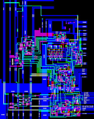
si8521r1_11b_sp_control.png [ 270.32 KiB | Viewed 1619 times ]

Attachment:
8521r1_11b_sp_control.png
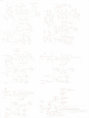
8521r1_11b_sp_control.png [ 411.98 KiB | Viewed 1619 times ]


Top
 Profile  
Reply with quote  
 Post subject: Re: 8521 dissection
PostPosted: Wed Nov 30, 2022 11:04 am 
Offline
User avatar

Joined: Fri Nov 09, 2012 5:54 pm
Posts: 1392
12) CNT edge detector

If there was a rising edge on the CNT pad,
it sets the high active signal CNT_EDGE to active in the next PHI2 cycle.

CNT_EDGE changes at PHI1.

The game is similar to what we already have seen in the "5a) FLAG#" and "5b) TOD pad" edge detectors.

;...

The low_active CNT# signal comes from "5e) CNT pad buffer\driver",
basically it's the signal from the CNT pad inverted by a Schmitt trigger.

So technically, the CNT edge detector (which is a falling edge detector)
scans the CNT pad for a rising edge.

CNT# directly goes into a NOR gate, together with the inverted/delayed CNT# signal
Inversion/delay is done by four "open collector" inverters (with pullup resistors
to VCC and capacitors to GND at their outputs) plus one normal inverter.

If there is a falling edge on the CNT# signal, the NOR gate emits a pulse
which sets the first RS flipflop. (The width of the pulse is set by the delay).

The first RS flipflop (built from two NOR gates) is cleared again,
if the high_active CNT_EDGE signal is active.

A multifunction gate contains the second RS flipflop,
which is gated at PHI2 for sampling the contents of the first RS flipflop.

The (inverted) output of the second RS flipflop is sampled by a transparent latch at PHI1.
The output of the latch goes through an inverter and becomes the CNT_EDGE signal,
which now nicely is synchronized with the system clock.

It is active for one PHI2 cycle after there was a rising edge on the CNT pad.

CNT_EDGE goes into:
"8c) timer A input carry generation",
"9c) timer B input carry generation",
"11b) serial port control".

Attachment:
si8521r1_12_cnt_edge.png
si8521r1_12_cnt_edge.png [ 39.22 KiB | Viewed 1619 times ]

Attachment:
8521r1_12_cnt_edge.png
8521r1_12_cnt_edge.png [ 148.99 KiB | Viewed 1619 times ]


Top
 Profile  
Reply with quote  
 Post subject: Re: 8521 dissection
PostPosted: Wed Nov 30, 2022 11:05 am 
Offline
User avatar

Joined: Fri Nov 09, 2012 5:54 pm
Posts: 1392
13) internal databus precharge

Since the outputs of the registers only are able of switching the internal
data bus D0io..D7io to GND, we need to have a "pullup" on D0io..D7io somewhere.

This part sits in the South West area of the chip.

In the 6530 and in the 6522, we had FETs which precharge the internal data bus
to HIGH during PHI1.

In the 8521 and in the 8520, it's different.

A voltage divider built from two big FETS sets the gate voltage of 8 smaller FETs,
which inject a current from VCC into the internal data bus 0io..D7io.

Obviously, the thumb rules for estimating the impedance of a FET in saturation
won't bring us far here, so please ignore the impedances in that part of the schematic.

Anyhow, for a FPGA\TTL\transistor implementation of the 8521,
how the internal data bus is pulled up to VCC is an academic question only.

Attachment:
si8521r1_13_precharge.png
si8521r1_13_precharge.png [ 26.34 KiB | Viewed 1619 times ]

Attachment:
8521r1_13_precharge.png
8521r1_13_precharge.png [ 8.56 KiB | Viewed 1276 times ]


Last edited by ttlworks on Mon Jan 08, 2024 2:58 pm, edited 1 time in total.

Top
 Profile  
Reply with quote  
 Post subject: Re: 8521 dissection
PostPosted: Wed Nov 30, 2022 11:19 am 
Offline
User avatar

Joined: Fri Nov 09, 2012 5:54 pm
Posts: 1392
14a) two TOD counter cells

In the 8521\6526, we have TOD (time of day), and it's a BCD up counter.
//BCD = binary coded decimal. It's a decimal up counter.

My end result for the 8521 TOD section looks like this:

Attachment:
8521r1_14_tod_section.png
8521r1_14_tod_section.png [ 281.34 KiB | Viewed 1615 times ]


;---

First a simple overview of what we are dealing with:

Attachment:
8521r1_14_tod_orientation.png
8521r1_14_tod_orientation.png [ 20.1 KiB | Viewed 1615 times ]


Code:
Six big boxes are BCD up counters, from East to West:
10THS //10ths seconds, 4 Bit counter, end count = $9
SL    //seconds low  , 4 Bit counter, end count = $9
SH    //seconds high , 3 Bit counter, end count = $5
ML    //minutes low  , 4 Bit counter, end count = $9
MH    //minutes high , 3 Bit counter, end count = $5
HL    //hours low    , 4 Bit counter, end count = $9


Circuitry of the counters is pretty similar to the binary TOD counters we had in the 8520,
except that in the 8520 end count is $F, and in the 8521 end count is $5\$9.

In the 8520 and 8521 counter cells, the counter Bits are present in inverted
and in non_inverted form.
A NOR gate inside the counter blocks (with the individual transistors distributed
amung the counter Bit cells) checks if the end count is reached,
and in the 8521 the inputs of said NOR gates are just creatively connected
to the inverting/non_inverting counter Bits in a different way than in the 8520.

The HL counter Block has an additional NOR gate which checks for $2,
that's because the real time clock has an AM\PM flag.

East of the 10THS counter block (14a), we have a box (14d)
which generates the low_active input carry for said BCD counter block.

Between the six BCD counter blocks, we have some more little boxes (14e).
For every counter block, there is some circuitry related to generating
counter control signals and counter input carry East and West of the BCD counter block.

However, the box (14h) between the SH and ML counter blocks
is a bit different from the other little (14e) boxes in that
there is a transparent PHI1 latch followed by a transparent PHI2 latch
inserted into the counter carry chain,
obviously the propagation delay of said carry chain became a bit too big
for one PHI2 clock cycle.

In the 8521, layout of said (14h) box is different from the layout in the 8520,
but from the logic design point of view there is no difference at transistor level.

The boxes (14b,14c) are responsible for disabling TOD increments
when the CPU writes the TOD_HR counter register
(and for enabling TOD increments when the CPU writes the TOD_10THS counter register),
for freezing the read data latches between TOD counters and internal data bus
when the CPU reads the TOD_HR read latch
(and for making the data read latches transparent again
when the CPU reads the TOD LSB_10THS read latch).

The box labeled 14g basically is an edge detector
which generates an ALARM_INT pulse when the values
in the TOD counter registers and in the ALARM registers
are starting to match.


Top
 Profile  
Reply with quote  
Display posts from previous:  Sort by  
Post new topic Reply to topic  [ 50 posts ]  Go to page Previous  1, 2, 3, 4  Next

All times are UTC


Who is online

Users browsing this forum: No registered users and 35 guests


You cannot post new topics in this forum
You cannot reply to topics in this forum
You cannot edit your posts in this forum
You cannot delete your posts in this forum
You cannot post attachments in this forum

Search for:
Jump to: