6502.org Forum  Projects  Code  Documents  Tools  Forum
It is currently Sat Apr 27, 2024 8:52 pm

All times are UTC


Post new topic Reply to topic  [ 50 posts ]  Go to page Previous  1, 2, 3, 4  Next
Author Message
 Post subject: Re: 8521 dissection
PostPosted: Wed Nov 30, 2022 11:21 am 
Offline
User avatar

Joined: Fri Nov 09, 2012 5:54 pm
Posts: 1392
14a) TOD two cells

Now to peek into the TOD Bit cells, the two uppermost Bits.

Carry for a 4 Bit block of TOD counter cells ripples through
in inverted/non_inverted form from East to West.

Note: the TOD counter Bit cells operate with the PHI20 clock.
PHI20 is HIGH at PHI2, in every fourth PHI2 cycle.
Means that TOD is clocked with PHI2/4.

South to North, we have:

;...

A transparent latch for reading the TOD counters from the CPU.
Data bus is 8 Bit, counter has more Bits than that,
counter still shold be counting while reading it,
so we can't get around having such latches.

In all TOD Bit cells, the high active control signal TOD_RSAMPLE
makes the latches sampling the values which are in the counters.
High_active control signal TOD_RHOLD makes the latches holding the data
(it also refreshes the contents of the half_static latches).

TOD_RSAMPLE and TOD_RHOLD are generated in "14b) TOD control logic".

High active register read control signals for the individual Bytes
of the read latches R_TOD_10THS, R_TOD_SEC, R_TOD_MIN, R_TOD_HR
are generated in "6) address decoder" (at PHI2).

;...

Next, we have the ALARM register Bits creatively crammed in.

Again we have half_static transparent latches, refreshed at PHI1,
written with high_active register write control signals
W_ALARM_10THS, W_ALARM_SEC, W_ALARM_MIN, W_ALARM_HR which are generated in
"6) address decoder" (at PHI2).

Active RES clears all ALARM registers at PHI1.

ALARM registers use a similar concept like the CRA, CRB registers,
it's just that the transparent latches controlled by PHI1
in the outputs of the ALARM registers (for preventing spikes
when writing the register) are creatively crammed into
the comparator section.

;---

Next, we have the TOD counter Bits.

Even Bits have low_active carry input, high_active carry output.
Odd Bits have high_active carry input, low_active carry output.

Carry input of a 4 Bit counter block changes with PHI20.

Count result is prepared at PHI1.

Counter outputs change when high_active clock signal TOD_CNT_10THS is active (changes at PHI20).
Note, that every 4 Bit block has its own TOD_CNT_* signal.

Counter Bits are cleared with high_active control signal TOD_CLR_10THS (changes at PHI20).
Note, that every 4 Bit block has its own TOD_CLR_* signal.

TOD_TC_10THS is a 5 input NOR gate which checks if the 4 Bit BCD counter
is in overflow condition ($9) while counting is enabled.

Note, that the HL (hour low) counter contains an additional NOR gate
which checks for $2, that's for the AM\PM flag.

;...

We now have reached the North of the TOD Bit cell,
and that's where the comparator sits.

Comparator basically uses XOR gates for comparing TOD counter register contents
with ALARM register contents, then pulls ALARM_EQ low if they don't match.

ALARM_EQ is a 24 input NOR gate, and its output goes into
"14g) TOD INT", where an edge detector generates the TOD_INT signal
when detecting a rising edge on ALARM_EQ,
for setting the ALARM interrupt flag.

;---

However, please note that the HL1 Bit is different.
While all of the other BCD counter Bits are cleared, HL1 is loaded with HH#.
HH# is the low_active output of the HH Bit, MSB of the hour counter.

That's for making TOD jumping from 12:59:59 to 01:00:00,
and we are getting to this trick later in "14f) HH PM".

;---

Attachment:
si8521r1_14a_tod_2cells.png
si8521r1_14a_tod_2cells.png [ 74.91 KiB | Viewed 1843 times ]

Attachment:
8521r1_14a_tod_2cells.png
8521r1_14a_tod_2cells.png [ 235.82 KiB | Viewed 1843 times ]


Top
 Profile  
Reply with quote  
 Post subject: Re: 8521 dissection
PostPosted: Wed Nov 30, 2022 11:23 am 
Offline
User avatar

Joined: Fri Nov 09, 2012 5:54 pm
Posts: 1392
14c) is just a NAND gate with push/pull output,
sensing if the CPU wants to read/write TOD_HR.

So I had integrated it into 14b).

Attachment:
si8521r1_14c_tod_ctrl2.png
si8521r1_14c_tod_ctrl2.png [ 6.05 KiB | Viewed 1844 times ]


;---

14b) TOD control

When TOD_10THS is written with high_active register write control signal W_TOD_10THS,
the "TOD count enable" RS flipflop is set at the start of the next PHI2 cycle,
what enables TOD counting with high_active signal TOD_STOP going LOW.

When the CPU writes TOD_HR, or when RES is active,
the "TOD count enable" RS flipflop (buit from two NOR gates) is cleared,
what disables TOD counting with high_active TOD_STOP signal going HIGH.
;
Note:
This means after RES was active, you would have to write TOD_10THS to enable TOD counting.

"Writing TOD_HR" means:
LOW_active write enable signal WE# is active, //generated in "2) CS#, R/W#"
High_active select signal SEL_$B is active, //generated in "6) address decoder"
CRB7 control register B Bit is 0.

TOD_STOP goes into the "5b) TOD predivider".
If TOD_STOP is HIGH, it stops/clears said predivider to disable TOD counting.

;...

When the CPU reads TOD_HR, the "TOD read sample/hold" RS flipflop
(built from two NOR gates) is set, and TOD_RHOLD goes active,
freezing the TOD read latches.

When the CPU reads TOD_10THS with high_active register read control signal R_TOD_LSB,
or when RES is active, the "TOD read sample hold" RS flipflop is cleared,
and TOD_RSAMPLE goes active, making the TOD read latches transparent again.

"Reading TOD_HR" means:
LOW_active read enable signal RD# is active, //generated in "2) CS#, R/W#"
High_active select signal SEL_$B is active, //generated in "6) address decoder"
CRB7 control register B Bit is 0.

;...

Short form:
TOD_HR write > disable TOD counting
TOD_10THS write > enable TOD counting //you have to do that after RES was active
TOD_HR read > freeze TOD read latches
TOD_10THS read > make TOD read latches transparent again.

Attachment:
si8521r1_14b_tod_control.png
si8521r1_14b_tod_control.png [ 48.29 KiB | Viewed 1844 times ]

Attachment:
8521r1_14b_tod_control.png
8521r1_14b_tod_control.png [ 193.24 KiB | Viewed 1844 times ]


Top
 Profile  
Reply with quote  
 Post subject: Re: 8521 dissection
PostPosted: Wed Nov 30, 2022 11:33 am 
Offline
User avatar

Joined: Fri Nov 09, 2012 5:54 pm
Posts: 1392
14 deh) TOD counter carry, and TOD counter control

That part looks a bit confusing in the silicon.

Note: the TOD counter Bit cells operate with the PHI20 clock.
PHI20 is HIGH at PHI2, in every fourth PHI2 cycle.
Means that TOD is clocked with PHI2/4.

I think that the designers intentionally did it this way
because the delay of the carry chain was too much
for running the counters at PHI2 speed...

;...

Attachment:
8521r1_14_tod_orientation.png
8521r1_14_tod_orientation.png [ 20.1 KiB | Viewed 1843 times ]


Code:
TOD BCD counter (plus read latches plus ALARM registeres plus comparator)
breaks into six blocks, from East (LSB) to West:
4 Bits 10THS: T1,T2,T4,T8     //10ths seconds
4 Bits SL:    SL1,SL2,SL4,SL8 //seconds low
3 Bits SH:    SH1,SH2,SH4     //seconds high
4 Bits ML:    ML1,ML2,ML4,ML8 //minutes low
3 Bits MH:    MH1,MH2,MH4     //minutes high
4 Bits HL:    HL1,HL2,HL4,HL8 //hours low


//HH and PM are a different story, which is covered later in 14f).

Every block has its own (low_active) carry input,
its high active count clock, and its high active clear.

Basicaly, chip layout for the 8521 TOD BCD counter and the 8520 binary counter
is pretty similar, just the overflow detection is different.

For simplifying things, let's take a look at the control logic for
the TOD SL counter.

We have "sort of" a parallel lookahead carry mechanism:
When the next lower counter (10THS) is cleared with TOD_CLR_10THS, this means:
the counter for 10THS is $9, counting for 10THS is enabled,
and the SL counter is supposed to increment
(when the counter for 10THS rolls over to $0).

TOD_CLR_10THS goes through an inverter, into a transparent latch clocked
with TOD_CNT_SL (same clock as for latches in counter SL),
the output of that transparent latch is the low_active carry input
for SL counter Bit SL1.
For inhibiting the carry input, the transparent latch is set when:
SL counter is cleared with TOD_CLR_SL,
or when the CPU writes the SL counter Bits with W_TOD_SEC at PHI2.
//when loading or clearing the counter, do not count.

TOD_CLR_SL becomes active when RES is active,
or when SL is $9 while TOD_CLR_10THS is active,
sampled at PHI20 by a transparent latch which is reset
when W_TOD_SEC is active.
//when loading the counter, don't clear it.

So the carry lookahead mechanism technically could be interpreted
as a chain of AND gates, where the TOD_CLR_* signals ripples through,
and four (or three) counter Bits go into every AND gate.

What complicates things:
When having "lump of logic" in the silicon between the BCD counter blocks,
logic for generating the control signals of one counter block
is in the "lumps of logic" at both sides of said counter Block.


Technically, from the logic design point of view what's between the counter blocks
(except for TOD SH > TOD ML) could be interpreted like this:

Attachment:
si8521r1_14e_tod_cin_sl1.png
si8521r1_14e_tod_cin_sl1.png [ 31.48 KiB | Viewed 1843 times ]

Attachment:
8521r1_14e_tod_cin_sl1.png
8521r1_14e_tod_cin_sl1.png [ 162.71 KiB | Viewed 1843 times ]


;---

14h) TOD ML counter ML1 input carry generation

The lump of logic between TOD SH and TOD ML is slightly different:

Basically, we have a transparent latch controlled by PHI1,
followed by another transparent latch controlled by PHI2,
inserted into the carry chain between TOD SH and TOD ML.

Attachment:
si8521r1_14h_tod_cin_ml1.png
si8521r1_14h_tod_cin_ml1.png [ 24 KiB | Viewed 1843 times ]

Attachment:
8521r1_14h_tod_cin_ml1.png
8521r1_14h_tod_cin_ml1.png [ 200.36 KiB | Viewed 1843 times ]


;---

14d) TOD 10THS counter T1 carry input generation

It's a bit smaller, because we don't need to check for an overflow
on the next lower BCD counter Block while counting is enabled...
because there is none.

AC mains frequency (50Hz or 60Hz) goes into the TOD pad.
"15b) TOD predivider" is counting rising edges at the TOD pad.
TOD predivider divides down the 50Hz or 60 Hz to 10Hz pulses
on signal TOD_DET1.

A rising edge detector scans TOD_DET1 for generating the T1 input carry.

Attachment:
si8521r1_14d_tod_cin_t1.png
si8521r1_14d_tod_cin_t1.png [ 32.85 KiB | Viewed 1843 times ]

Attachment:
8521r1_14d_tod_cin_t1.png
8521r1_14d_tod_cin_t1.png [ 124.09 KiB | Viewed 1843 times ]


Top
 Profile  
Reply with quote  
 Post subject: Re: 8521 dissection
PostPosted: Wed Nov 30, 2022 11:35 am 
Offline
User avatar

Joined: Fri Nov 09, 2012 5:54 pm
Posts: 1392
14f) HH, TOD

In the 8521, TOD is a 12-hour clock.
//in the 8520, there is no HH, TOD in the silicon.

//a.m. (from Latin ante meridiem, translating to "before midday")
//p.m. (from Latin post meridiem, translating to "after midday").

We have two one_Bit counter cells, labelled HH and PM (both of them have identical layout),
which are just a variation from the one_Bit counter cells
we had for generating the shift register clock in "11) SP control"
and for generating the PB6,PB7 square wave signal in "8e) 9e) timer control logic".
;
A rising edge on the toggle signal flips the Bit.

HH is the MSB of the hour counter. //Hour counter is HL1,HL2,HL4,HL8,HH.
PM is the AM\PM flag. //also a one_Bit counter.

When HL counter has to be incremented (because the MH counter output carry is active)
and HL counter already is $9 while HH=0, HL is cleared to $0 and HH is set to 1.

When HL counter has to be incremented (because the MH counter output carry is active)
and HL counter already is $2 while HH=1 (when hours = decimal 12), HL is set to $1 and HH is cleared.

When the hour counter reaches 12, PM toggles.
Note, that the ML output carry doesn't go into the equation,
so writing decimal 12 into the hours if the hours already were not 12 this will toggle PM.

//And please take a look at wikipedia Confusion at noon and midnight.

Also, we have the ALARM registers ALARM_HH and ALARM_PM,
and the related comparators.
;
Chip layout of that part is different from the ALARM registers
and comparators we had in the rest of the BCD counters,
but at logic design level the transistor level schematics are identical.

So far for the simple version.

;...

PM flag:

We have sort of a comparator which checks if HH=1 and if HL=$2.
The rising edge of the comparator output toggles the PM flag.
Again, note that the MH output carry doesn't go into this.

The PM flag toggles when TOD reaches 12:00:00, that yes.

But a side effect is that when writing "HH=1 and HL=$2" to the TOD_HR register,
and the TOD_HR register previously was not "HH=1 and HL=$2", this toggles the PM flag.
In this case, you would have to write with the PM Bit _inverted_ into the TOD_HR register
to compensate for this.

;...

HL1 Bit and HH#:

TOD jumps from 12:59:59 to 01:00:00.

For implementing this, the designers had pulled a trick.

If there was an overflow in the MH counter,
and either HH=0 AND HL=$9, or HH=1 AND HL=$2,
the high_active control signal TOD_CLR_ML
clears the Bits HL8,HL4,HL2 and loads HL1 with HH#.

But wait a minute:
Wouldn't this make TOD jump from 09:59:59 to 11:00:00 and from 12:59:59 to 00:00:00 ?

After checking that water still flows from out of the water tap down into the basin,
and that a screwdriver still falls toward the mass center of planet Earth when getting dropped,
I felt a need to take a closer look at why the designers had used HH# instead of HH.

The trick is hidden within the timing.
The HL+HH overflow is sampled by a transparent latch at PHI20
(which is high at PHI2 in every fourth PHI2 clock cycle)
for generating the TOD_CLR_HL signal which loads HH# into HL1.

TOD_CLR_HL is sampled by another transparent latch at PHI1,
for generating the TOGGLE_HH signal.
A rising edge on TOGGLE_HH signal flips the HH counter Bit.

So TOD_CLR_HL changes half a PHI2 cycle _before_ TOGGLE_HH changes.

This means, that for 0.5 PHI2 cycles, the wrong HH value is written into HL1,
and for 3.5 PHI2 cycles (after HH has toggled) the _correct_ HH value is written into HL1.
But you won't notice from the state of the HL1 Bit (except for a 0.5 PHI2 cycle delay).
//A nice trick for saving some logic gates.

And that's why TOD indeed jumps from 09:59:59 to 10:00:00 and from 12:59:59 to 01:00:00,
I had checked this on a real C64 by resorting to peek() and poke() just to be on the safe side...

;...

Attachment:
si8521r1_14f_tod_hh_pm.png
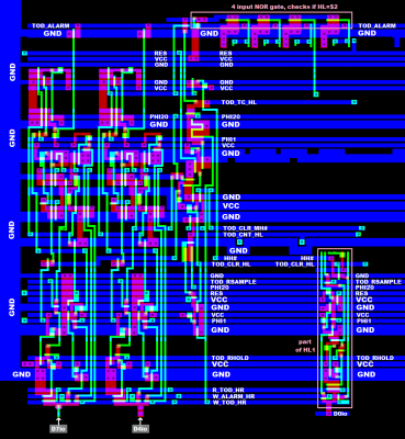
si8521r1_14f_tod_hh_pm.png [ 77.13 KiB | Viewed 1843 times ]

Attachment:
8521r1_14f_tod_hh_pm.png
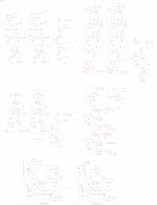
8521r1_14f_tod_hh_pm.png [ 232.1 KiB | Viewed 1843 times ]


Top
 Profile  
Reply with quote  
 Post subject: Re: 8521 dissection
PostPosted: Wed Nov 30, 2022 11:36 am 
Offline
User avatar

Joined: Fri Nov 09, 2012 5:54 pm
Posts: 1392
14g) TOD INT

Note: the TOD counter Bit cells operate with the PHI20 clock.
PHI20 is HIGH at PHI2, in every fourth PHI2 cycle.
Means that TOD is clocked with PHI2/4.

High_active signal ALARM_EQ is generated by a 24 input NOR gate,
which is distributed among all of the TOD comparator cells
(comparing the TOD counter Bits with the ALARM register Bits).
The pullup resistor (FET) of this NOR gate is integral part of 14g).

If the values in the TOD counter Bits match the values
in the ALARM register Bits, ALARM_EQ is HIGH.

ALARM_EQ is sampled by a transparent latch at PHI20,
then by another transparent latch at PHI1,
then goes into a rising edge detector.

When a rising edge is detected, high_active signal TOD_INT
goes active for one PHI2 cycle,
what sets the ALARM interrupt flag.

;...

Attachment:
si8521r1_14g_tod_int.png
si8521r1_14g_tod_int.png [ 17 KiB | Viewed 1843 times ]

Attachment:
8521r1_14g_tod_int.png
8521r1_14g_tod_int.png [ 85.05 KiB | Viewed 1843 times ]


Top
 Profile  
Reply with quote  
 Post subject: Re: 8521 dissection
PostPosted: Wed Nov 30, 2022 11:38 am 
Offline
User avatar

Joined: Fri Nov 09, 2012 5:54 pm
Posts: 1392
To me, it feels like Frank and me want a bit too fast with that 8521 dissection.
Sorry if the quality of our dissection might have been affected by this.

Hi Dani, good luck with your TTL 6526 implementation. :)

That's all for now,
and 6520 is next.


Last edited by ttlworks on Wed Dec 07, 2022 10:47 am, edited 1 time in total.

Top
 Profile  
Reply with quote  
 Post subject: Re: 8521 dissection
PostPosted: Wed Nov 30, 2022 11:55 am 
Offline

Joined: Thu Jul 20, 2017 9:58 am
Posts: 91
ttlworks wrote:
To me, it feels like Frank and me want a bit too fast with that 8521 dissection.
Sorry if the quality of our dissection might have been affected by this.


I can only speak for me: The creation of the 8521 was a lot of copy&paste from the previous 8520.
Assuming that the differences are much less than they really are I was rather sloppy
in my efforts... :oops:

TLDR; The 8521 was my worst work until today... the next ones will (are) be better! Promised!


Top
 Profile  
Reply with quote  
 Post subject: Re: 8521 dissection
PostPosted: Wed Nov 30, 2022 11:56 am 
Offline

Joined: Fri Jan 25, 2019 2:29 pm
Posts: 191
Location: Madrid, Spain
ttlworks wrote:
To me, it feels like Frank and me want a bit too fast with that 8521 dissection.
Sorry if the quality of our dissection might have been affected by this.


I don't think there are many people in the world with enough knowledge and commitment to do this better.

ttlworks wrote:
Hi Dani, good luck with your TTL 6526 implementation. :)


I've been lurking the thread since you started posting earlier today :D

PCBs for SDR and ICR just landed in Paris. Plenty of work ahead.

Thanks you for this work. It just never stops impressing me.


Top
 Profile  
Reply with quote  
 Post subject: Re: 8521 dissection
PostPosted: Wed Nov 30, 2022 12:06 pm 
Offline

Joined: Thu Jul 20, 2017 9:58 am
Posts: 91
daniMolina wrote:
Thanks you for this work. It just never stops impressing me.


:D

Keeping fingers crossed that everything works with your TTL6526 until the day the VIC-II dissection is finished
(if this will ever happen... :wink: )
Seeing a VIC-II built from TTL chips will be even more impressing.


Top
 Profile  
Reply with quote  
 Post subject: Re: 8521 dissection
PostPosted: Wed Nov 30, 2022 1:19 pm 
Offline
User avatar

Joined: Thu Dec 11, 2008 1:28 pm
Posts: 10793
Location: England
Most impressive, and as ever, thanks for sharing. Needless to say, I have not digested all the information presented! But it is always very nice to see little quirks and oddities coming from the transistors.


Top
 Profile  
Reply with quote  
 Post subject: Re: 8521 dissection
PostPosted: Wed Nov 30, 2022 4:48 pm 
Offline

Joined: Wed Jul 27, 2022 9:27 pm
Posts: 5
Very nice. These are all loose fragments - is there a comprehensive diagram (svg) of diffusion+poly somewhere? Or else just a die shot that is detailed enough so that it can be verified by nerds that don't have anything better to do? :)


Top
 Profile  
Reply with quote  
 Post subject: Re: 8521 dissection
PostPosted: Wed Nov 30, 2022 5:05 pm 
Offline
User avatar

Joined: Thu Dec 11, 2008 1:28 pm
Posts: 10793
Location: England
(oh, welcome, mathop!)


Top
 Profile  
Reply with quote  
 Post subject: Re: 8521 dissection
PostPosted: Thu Dec 01, 2022 7:22 am 
Offline
User avatar

Joined: Fri Nov 09, 2012 5:54 pm
Posts: 1392
Hi mathop,
A microscopic picture of the 8521R0 can be found here.

Frank pays 2k€ layoratory costs for decapping a chip and getting a microscopic picture,
then spends months with manually polygonizing said picture with Inkscape.
He had made some bad experiences with people stealing his work in the past.

So if you really need the polygonized 8521R1 picture which was the base for our 8521R1 dissection at full resolution,
you probably would have to sign sort of a NDA, then to negotiate with Frank for the price, sorry.

Your other options would be either to wait until Frank eventually puts his pictures in the open...
...or to join our team. :)

BTW: Frank's other hobby is building/selling FPGA plugin replacements for Commodore chips.
My dissection schematics are the reference for a sanity check if something goes wrong within his FPGA toolchain.


Top
 Profile  
Reply with quote  
 Post subject: Re: 8521 dissection
PostPosted: Thu Dec 01, 2022 8:30 am 
Offline

Joined: Thu Jul 20, 2017 9:58 am
Posts: 91
ttlworks wrote:
....
BTW: Frank's other hobby is building/selling FPGA plugin replacements for Commodore chips.


Just a small correction:

Building replacements -> YES!
Selling replacements -> Not really... as soon as it's working I'm looking for new technical challenges. :D
I usually leave selling stuff to other people that are better businessmen than I am. :mrgreen:


Top
 Profile  
Reply with quote  
 Post subject: Re: 8521 dissection
PostPosted: Thu Dec 22, 2022 9:43 am 
Offline
User avatar

Joined: Tue Jun 07, 2016 4:34 pm
Posts: 53
Nice job guys! An interesting read, I've already found some useful bits.
Looking forward to the VIC-II dissection.


Top
 Profile  
Reply with quote  
Display posts from previous:  Sort by  
Post new topic Reply to topic  [ 50 posts ]  Go to page Previous  1, 2, 3, 4  Next

All times are UTC


Who is online

Users browsing this forum: No registered users and 36 guests


You cannot post new topics in this forum
You cannot reply to topics in this forum
You cannot edit your posts in this forum
You cannot delete your posts in this forum
You cannot post attachments in this forum

Search for:
Jump to: