6502.org Forum  Projects  Code  Documents  Tools  Forum
It is currently Thu May 02, 2024 1:18 am

All times are UTC


Post new topic Reply to topic  [ 7 posts ] 
Author Message
PostPosted: Tue May 23, 2023 7:15 pm 
Offline
User avatar

Joined: Fri Feb 17, 2023 11:59 pm
Posts: 163
Location: Lviv, Ukraine
I'm using W65C22N (yes, NMOS-compatible version), I bought it from Mouser, so it must be a modern part.

(My 6551 is also W65C51N - I preferred them over CMOS versions because of open-drain /IRQ that can be wire OR'ed, and also because I want them to be compatible with some of my other NMOS chips that I might be adding to my SBC).

I'm reading PS/2 in a bit-banging fashion through 65C22N:
- PS/2 data -> PB4
- PS/2 clock -> CB2

I have my VIA fire an interrupt on the falling edge of CB2:
Code:
        lda #%01111111  ; Disable all interrupts
        sta VIA1_IER
        lda #%10001000  ; Set interrupt flag for CB2 (page 27)
        sta VIA1_IER

My ISR then counts 11 bits and registers a "key pressed/released" flag.

However I'm sometimes getting weird /IRQ assertions when pressing keys on a keyboard (happens <1% of time, but is annoying as hell):

Attachment:
phantom_irq.png
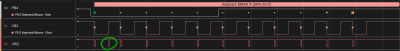
phantom_irq.png [ 23.4 KiB | Viewed 875 times ]


The green circle shows a place where /IRQ is asserted despite CB2 is rising. You can clearly see that it's aligned with CB2. This results in clock skew, so now all my PS/2 packets are off by 1 bit. This happens in random places.

- My /IRQ is pulled up with 5K resistor. Same issue is reproducible with my another SBC which has a 3.3K pull-up.
- Both PS/2 lines are pulled up with 1K resistors.
- No other hardware is using /IRQ - it's wired only from 65C22N to 65C02S (I've removed 65C51N for debugging.)
- My ISR takes ~4us to clear VIA's interrupt flag (I'm doing that as early as possible) and you can clearly see that the /IRQ line is released normally.
- This seems to occur much more frequently when I rapidly slam my keyboard. However, my logic analyzer still properly decodes PS/2 packets.
- I'm running @ 8 MHz.

Why could this be happening?

EDIT: This is also reproducible with another keyboard AND with another revision of my SBC (which has totally different PCB traces, so I highly doubt that crosstalk is involved.)
<s>EDIT 2: I'm going to try another VIA for this. That's the only part I've reused in both builds. I highly doubt that it's my software that's guilty - the code is very simple.</s> nope - same issue with a different W65C22N.
EDIT 3: Could it be due to mixing W65C02S & W65C22N?
EDIT 4: I think I should replace my 'N chips with 'C versions and join IRQ lines through 74HC08 (or 74HC11 to have an extra line for open-drain chips.)

_________________
/Andrew

deck65 - 6502 slab with screen and keyboard | ПК-88 - SBC based on KM1810VM88 (Ukrainian i8088 clone) | leo80 - simple Z80 SBC
nice65 - 6502 assembly linter | My parts, footprints & 3D models for KiCad/FreeCAD


Top
 Profile  
Reply with quote  
PostPosted: Tue May 23, 2023 8:45 pm 
Offline

Joined: Sun May 13, 2018 5:49 pm
Posts: 247
and3rson wrote:
However I'm sometimes getting weird /IRQ assertions when pressing keys on a keyboard (happens <1% of time, but is annoying as hell):
Why could this be happening?
It's most likely an actual falling edge at the CB2 pin - from the perspective of the 65C22. Do you have an oscilloscope? If so, you want to look at CB2 with the scope probe using the 65C22's VSS pin as the ground reference. My guess is signal or ground bounce - the latter might look like the CB2 trace dips even though it's actually a rise on the ground line instead.

Is this on your V15 65ad02 board? If so, the power and ground traces appear super-thin on that board, and I don't see any cap next to the PS/2 connector for the power sent to the keyboard. I'm also having a hard time tracing the GND connection from the bypass cap C9 to the VSS pin of the 65C22 (using the photos and diptrace screenshot you posted earlier). You may want to solder a 0.1uF ceramic cap directly across the VSS/VDD pins of the 65C22 on the back (or top, if you prefer) of your board. It's a bit of a stretch on that IC, so you may need to "extend" one of the legs, but you want the connections between the bypass cap and the IC to be as short as physically possible. If the traces are too long between the bypass cap and the VCC/VSS pins of the IC you are trying to bypass, then the cap is unable to do the job.

If you don't have a scope to look at what CB2 is actually seeing (a logic analyzer may not catch it), you might want to also try beefing up the power and ground to the keyboard (eg. solder wire from connector over to regulated power for power and ground, and add a bulk cap (actual value not too important - perhaps 100uF) and 0.1 ceramic bypass cap). You may also want to beef up the ground connection between 65C22 and the PS/2 port, as those need to stay close to each other and if one or the other moves too much it could create a "phantom" falling edge. PS/2 keyboards can pull up to 100mA (modern keyboards often draw less, but some older ones draw even more than that) and the power traces should be sized for that. The signal traces can be thin and that's generally not an issue.

If this is a different board, then can you send photos of your setup?


Top
 Profile  
Reply with quote  
PostPosted: Wed May 24, 2023 3:39 pm 
Offline
User avatar

Joined: Fri Dec 11, 2009 3:50 pm
Posts: 3350
Location: Ontario, Canada
I agree with SamCoVT that, from the VIA's point of view, there probably is a falling edge at the CB2 pin. Of course the overall trend is to rise, but within that rising waveform there's a low-amplitude "kink" -- an instant during which the voltage actually lowers then resumes its upward direction. This is the result of noise superimposed on the desired signal.

I can think of some low-effort remedies that might reduce the noise, and Sam has touched on some of those. Some experimentation may be required.

But if you want to proceed directly to a solution, IMO your surest bet of success is to add a 74HC14 or 'HC132 Schmitt-trigger IC between the incoming Clk signal and the CB2 pin. (Since the '14 and the '132 invert, you could use two successive sections in order to restore the expected polarity. Or, alter your code to accept the new polarity, in which case you only need a single gate. That means you could save a lot of space by using a delightfully tiny '1G Series Schmitt.)

Incidentally, the -N type VIA is more susceptible to noise than the -S version. This is not about the /IRQ output; it's because all inputs on the N version are TTL compatible, which is to say they require a fairly small voltage swing (a swing from .8V to 2V or less) to respond. This means it takes only a small amount of noise to (mis-)trigger them. By comparison, the S version has better noise immunity because it's designed to accept CMOS levels (not TTL) and thus requires a larger voltage swing to respond. So, if you're reluctant to add a Schmitt, one experiment that'd be worthwhile is to try using an S type VIA.

BTW, this noise immunity issue could explain why your Logic Analyzer doesn't display the noise glitch.

-- Jeff

Edit: 'HC132, not 'HC32

_________________
In 1988 my 65C02 got six new registers and 44 new full-speed instructions!
https://laughtonelectronics.com/Arcana/ ... mmary.html


Last edited by Dr Jefyll on Wed May 24, 2023 9:39 pm, edited 1 time in total.

Top
 Profile  
Reply with quote  
PostPosted: Wed May 24, 2023 8:01 pm 
Offline
User avatar

Joined: Fri Aug 30, 2002 1:09 am
Posts: 8429
Location: Southern California
I give a description of what causes the groundbounce at viewtopic.php?p=55450#p55450 .  Even if the VIA isn't outputting data at the particular instant you're occasionally seeing the trouble, a nearby device could be, whether it's a memory IC or even the processor switching a lot of address lines at once, like to go from $C7FFF to $C800, or reading an instruction's operand at $C7FF followed by the address of a variable low in ZP.  There's more about how to remedy the problem in the first point in the AC-performance page of the 6502 primer at http://wilsonminesco.com/6502primer/construction.html .  It could be that just adding shorter connections between ICs' ground pins (and maybe power pins too) will be all that's needed to correct the problem.

There are other differences between the W65C22N and W65C22S besides just the IRQ\ output; so I encourage using the S version wherever practical.

_________________
http://WilsonMinesCo.com/ lots of 6502 resources
The "second front page" is http://wilsonminesco.com/links.html .
What's an additional VIA among friends, anyhow?


Top
 Profile  
Reply with quote  
PostPosted: Wed May 24, 2023 8:27 pm 
Offline

Joined: Sun May 13, 2018 5:49 pm
Posts: 247
It's also worth noting that the PS/2 protocol uses an open collector bus. This uses transistors to pull the line low and uses pullup resistors to pull the line high when they aren't actively being driven low by either the computer or the keyboard. Because the pullups are a weaker "pull", the rise time will be much longer on a rising edge than the corresponding falling edge.

I see in the W65C22 datasheet that CB2 has a MAX rise/fall time of 70ns and this likely isn't being met on the rise time if the pullup is weak (eg. 10K or larger). That would be another argument for adding the Schmitt-trigger IC between the CLK from the keyboard and the 65C22, as that would help to give nice crisp rising and falling edges. I agree with Jeff's recommendation of the HC family of logic, as it's reasonably fast but still slow enough that there won't be as much ringing on a transition.

If you don't have an oscilloscope to be able to measure things, I'd try the easy modifications first, one at a time, and test to see if the problem is better or worse (report back if one of these makes things worse, as that can be important too):
  1. Make sure you have a bypass cap (0.1uF) on the 65C22 with the leads as short as possible.
  2. Make sure the ground connection between the PS/2 port and 65C22 is short (eg. solder a direct wire). It wouldn't hurt to connect the +5V directly between them as well.
  3. Add some bulk capacitance to your board (eg. 100uF) on the 5V rail. Where exactly this gets placed probably isn't important.
  4. Reduce the resistance of your pullup resistor on the clock line to something like 3.3K or less if it's currently 10K or higher. I wouldn't recommend going under 1K.
  5. Add Schmitt-trigger to circuit - this helps reject noise AND make a nice fast rising edge

I see Garth mentioned his construction page, and there is a lot of good reading material in there. I don't think you'll need to get into terminating this line or changing to a multilayer board or anything like that, and you should be able to get your current board working properly. You don't need to eliminate ringing or ground bounce, but you might need to reduce it to a tolerable level where it no longer causes your glitch.


Top
 Profile  
Reply with quote  
PostPosted: Thu May 25, 2023 7:35 pm 
Offline
User avatar

Joined: Fri Feb 17, 2023 11:59 pm
Posts: 163
Location: Lviv, Ukraine
Thank you for all your replies!

SamCoVT - yes, it's almost the same as my V15 design - I'm on V16 already, haven't posted it yet, but it's almost exact same. :)

I've spent some time incorporating what your suggested (by beefing up the power & adding more capacitors), and I was actually able to reduce the noise to tolerable level - it's really hard to reproduce the problem now!

I've also noticed that it happens mostly during access to uSD card, so I think there may really be some ground bounce due to SD Card bending the ground.

I've decided to manually route power & UART lines with thicker traces manually, and leave the rest of the routing to Diptrace. Unfortunately, Diptrace still doesn't properly import Kicad netclasses - it merges them all in one. Not a problem though, since I routed all critical lines by hand.

Jeff - great idea, I'll include 74HC14 for my PS2 clock line in V17 build!

Garth - I've ordered 65C22S from Mouser yesterday, will give it a try and see if anything changes - I'm really curious if the issue will go away. But I'll try to stick to CMOS version in future anyway.

I've also moved ACIA, VIA, PS/2 connector, and ESP8266 as close as possible to each other and added more bypass & decoupling caps.

BTW - I was surprised there's no CMOS version 65C51, only 65C51N.

Last but not least - my ACIA is also messing stuff up: works fine with USB-UART adapter, but has issues with ESP8266 (even though I've added level shifting with 2N7000). I'll have my new PCB printed and see if the issue is still there: it really felt like crosstalk: TX line was getting corrupted when I accessed LCD while TX was low. The spikes were 1/2 cycles long, so I think there's some interference with LCD/EN or one of the address lines.

Manual routes:
Attachment:
File comment: I routed some main lines manually
v17_unrouted.png
v17_unrouted.png [ 412.05 KiB | Viewed 739 times ]


Diptrace for all the rest:
Attachment:
File comment: Diptrace did the rest of the job!
v17_routed.png
v17_routed.png [ 84.11 KiB | Viewed 739 times ]

Attachment:
v17_routed_back.png
v17_routed_back.png [ 82.93 KiB | Viewed 738 times ]


My board is a mess! :D
Attachment:
v16_mess.jpg
v16_mess.jpg [ 232.26 KiB | Viewed 738 times ]

_________________
/Andrew

deck65 - 6502 slab with screen and keyboard | ПК-88 - SBC based on KM1810VM88 (Ukrainian i8088 clone) | leo80 - simple Z80 SBC
nice65 - 6502 assembly linter | My parts, footprints & 3D models for KiCad/FreeCAD


Top
 Profile  
Reply with quote  
PostPosted: Thu May 25, 2023 8:26 pm 
Offline

Joined: Sun May 13, 2018 5:49 pm
Posts: 247
and3rson wrote:
I've spent some time incorporating what your suggested (by beefing up the power & adding more capacitors), and I was actually able to reduce the noise to tolerable level - it's really hard to reproduce the problem now!

I've also noticed that it happens mostly during access to uSD card, so I think there may really be some ground bounce due to SD Card bending the ground.

I've decided to manually route power & UART lines with thicker traces manually, and leave the rest of the routing to Diptrace. Unfortunately, Diptrace still doesn't properly import Kicad netclasses - it merges them all in one. Not a problem though, since I routed all critical lines by hand.
I'm glad to hear you were able to improve the situation, and that would seem to indicate that it is indeed a ringing or ground bounce type of issue.

Your CPU, RAM, and SDcard would also enjoy those wider power and ground traces. Adding a bypass cap at your SDcard socket may also help if you suspect it may be causing problems. They are designed for high speed operation and their current consumption can also vary during use, so it certainly could be causing ground bounce issues.

Your bypass connections on ICs look much improved. They would benefit very slightly from being wider traces as well, but it's not as important as having short connections. Did you switch to axial 0.1uF caps to fit them inside the sockets like that?

You may want to double-check the trace to pad clearance on C18 with it's square pad - I only see one pixel and can't tell if it has good clearance or not. It just caught my eye.

With the other changes you are planning to make, I think you will be in good shape for solving this particular issue.


Top
 Profile  
Reply with quote  
PostPosted: Thu May 25, 2023 9:18 pm 
Offline
User avatar

Joined: Fri Aug 30, 2002 1:09 am
Posts: 8429
Location: Southern California
The rule about making power and ground traces wider was applicable for the power-hungry TTL circuits of decades ago which used many amps of DC current and needed big power supplies and produced a lot of heat.  But for our low-power, higher-speed CMOS circuits, the "rule" is a myth, because our greater enemy is inductance, not resistance, and widening the traces has almost no effect on inductance.  Please see my post at viewtopic.php?p=94626#p94626 .  In your manual-routes picture, you should run another trace from ACIA1's pin 15 to U6's pin 20, making a good short-cut.  Do the same kind of thing from the processor to RAM1, ROM1, etc..

_________________
http://WilsonMinesCo.com/ lots of 6502 resources
The "second front page" is http://wilsonminesco.com/links.html .
What's an additional VIA among friends, anyhow?


Top
 Profile  
Reply with quote  
PostPosted: Fri May 26, 2023 12:00 pm 
Offline
User avatar

Joined: Fri Feb 17, 2023 11:59 pm
Posts: 163
Location: Lviv, Ukraine
SamCoVT wrote:
Your CPU, RAM, and SDcard would also enjoy those wider power and ground traces. Adding a bypass cap at your SDcard socket may also help if you suspect it may be causing problems. They are designed for high speed operation and their current consumption can also vary during use, so it certainly could be causing ground bounce issues.

Your bypass connections on ICs look much improved. They would benefit very slightly from being wider traces as well, but it's not as important as having short connections. Did you switch to axial 0.1uF caps to fit them inside the sockets like that?


I've added another bypass cap for uSD card - that thing could definitely have been a bottleneck!
I'm not using axial caps here - just ceramic discs, the reason why the holes are so far apart is that I wanted to have an extra "pass through" space under them, so I'm simply spreading their legs during assembly as such:
Attachment:
cap_spread.png
cap_spread.png [ 80.31 KiB | Viewed 691 times ]

This allows traces to run traces under the "hovering" cap on the same layer - I've seen a silimar technique being used with SMD 0-R resistors as jumpers to cross two traces on the same layer. This way I need less vias in case Diptrace decides to route a bunch of data lines through my chip.
They also fit nicely inside the machine-tooled socket, so I can keep them on the same side of the board as the IC, right under it.
Of course, this would become redundant with 4-layer boards.

SamCoVT wrote:
You may want to double-check the trace to pad clearance on C18 with it's square pad - I only see one pixel and can't tell if it has good clearance or not. It just caught my eye.
With the other changes you are planning to make, I think you will be in good shape for solving this particular issue.

Thanks! Yeah, it's outside of hole courtyard and is passing the DRC, so it should be good.

Updated routing:
Attachment:
v17b_unrouted.png
v17b_unrouted.png [ 241.93 KiB | Viewed 691 times ]

Diptrace saves the day, as usual:
Attachment:
File comment: 10 mil trace width, 10 mil clearance
v17b_routed.png
v17b_routed.png [ 125.67 KiB | Viewed 691 times ]


GARTHWILSON wrote:
The rule about making power and ground traces wider was applicable for the power-hungry TTL circuits of decades ago which used many amps of DC current and needed big power supplies and produced a lot of heat. But for our low-power, higher-speed CMOS circuits, the "rule" is a myth, because our greater enemy is inductance, not resistance, and widening the traces has almost no effect on inductance. Please see my post at viewtopic.php?p=94626#p94626 . In your manual-routes picture, you should run another trace from ACIA1's pin 15 to U6's pin 20, making a good short-cut. Do the same kind of thing from the processor to RAM1, ROM1, etc..


Thanks for the feedback - I've added this trace as well as merged the rest of chips together so that now I have all important IC grounds properly connected!

_________________
/Andrew

deck65 - 6502 slab with screen and keyboard | ПК-88 - SBC based on KM1810VM88 (Ukrainian i8088 clone) | leo80 - simple Z80 SBC
nice65 - 6502 assembly linter | My parts, footprints & 3D models for KiCad/FreeCAD


Top
 Profile  
Reply with quote  
PostPosted: Fri May 26, 2023 12:40 pm 
Offline

Joined: Sun May 13, 2018 5:49 pm
Posts: 247
GARTHWILSON wrote:
The rule about making power and ground traces wider was applicable for the power-hungry TTL circuits of decades ago which used many amps of DC current and needed big power supplies and produced a lot of heat.  But for our low-power, higher-speed CMOS circuits, the "rule" is a myth, because our greater enemy is inductance, not resistance, and widening the traces has almost no effect on inductance.
Thanks for linking your thread on the trace width vs inductance, Garth. I was trying to locate that but ran out of time. The circuits I design are mostly power converters, so I always like big traces for power and ground :)

And3erson, one thing you will find as you design more circuit boards is that you will be trying to balance/optimize at least 5 different things and often you can make one thing better at the expense of making at least two things worse. This is actually the part I enjoy about designing circuit boards. It's a bit of a game, and it really just needs to be "good enough" at the end of the day.

This board design looks much improved. I'll still call attention to the traces that are very close to pads. The soldermask registration isn't always spot on when the boards are made and most board houses require 4 mils larger soldermask openings around pads so they can be up to 4 mils off. The issue is that, if the soldermask is 4 mils off, it will open up 8 mils on one side and potentially expose a trace there. The board is still functional, but there is a danger during soldering that you might accidentally short to the exposed trace. I've had this happen on a production board, so I try keep traces at least 8 mils away from pads. Do you need to make this change on your board? - probably not. You're only making a few, and if you do see a misaligned soldermask layer you can just take care with soldering. That cap just made my spidey senses tingle because it's power and ground there.


Top
 Profile  
Reply with quote  
PostPosted: Fri May 26, 2023 10:25 pm 
Offline
User avatar

Joined: Fri Feb 17, 2023 11:59 pm
Posts: 163
Location: Lviv, Ukraine
SamCoVT wrote:
It's a bit of a game, and it really just needs to be "good enough" at the end of the day.

This board design looks much improved. I'll still call attention to the traces that are very close to pads. The soldermask registration isn't always spot on when the boards are made and most board houses require 4 mils larger soldermask openings around pads so they can be up to 4 mils off. The issue is that, if the soldermask is 4 mils off, it will open up 8 mils on one side and potentially expose a trace there. The board is still functional, but there is a danger during soldering that you might accidentally short to the exposed trace. I've had this happen on a production board, so I try keep traces at least 8 mils away from pads. Do you need to make this change on your board? - probably not. You're only making a few, and if you do see a misaligned soldermask layer you can just take care with soldering. That cap just made my spidey senses tingle because it's power and ground there.


Thank you!
You're totally right - I've moved it away just to be on the safe side, since I've seen my local vendor slightly offsetting drilled/milled holes, so I'm afraid they might mess it up as well. Better safe than sorry!
Attachment:
v17c_routed.png
v17c_routed.png [ 222.32 KiB | Viewed 642 times ]

_________________
/Andrew

deck65 - 6502 slab with screen and keyboard | ПК-88 - SBC based on KM1810VM88 (Ukrainian i8088 clone) | leo80 - simple Z80 SBC
nice65 - 6502 assembly linter | My parts, footprints & 3D models for KiCad/FreeCAD


Top
 Profile  
Reply with quote  
PostPosted: Sat May 27, 2023 3:56 pm 
Offline
User avatar

Joined: Fri Feb 17, 2023 11:59 pm
Posts: 163
Location: Lviv, Ukraine
So while waiting for my new PCB, I've tried to fix as much as possible in my current board, and I pretty much got things working almost stable!

- Added all the bypass caps as mentioned previously
- Added electrolytic caps next to power-hungry devices
- Cut TX/RX/GND traces between ACIA & ESP8266 (they are on opposites sides of the board) and wired them directly - this resolved all UART issues. I can't believe UART lines were so sensitive: what's even worse - things were working when I connected logic analyzer, but failed to do so when I disconnected the probes! But now it works all the time. I've also kept 2N7000 level shifting on ESP8266 TX line.
- Added 2x 74HC14 on PS/2 clock line.

I wrote a simple serial terminal program for my SBC, and so I managed to connect it to this cool new fancy thing called The Internet! Has anyone heard about it? :D

I'm using https://github.com/dhansel/WifiModem for ESP8266 which emulates a Hayes-compatible modem and allows me to use AT commands to go online.

I'm also added a 256-byte ring buffer to my ACIA/UART implementation, since screen scrollling sometimes took too long and thus I was losing 3-4 bytes from ACIA RX buffer on every scroll.

Here's me connecting to telehack.com:

Attachment:
telehack1.jpg
telehack1.jpg [ 176.84 KiB | Viewed 612 times ]

Attachment:
telehack2.jpg
telehack2.jpg [ 168.09 KiB | Viewed 612 times ]

Attachment:
File comment: GeoIP reports me being in Dnipro, even though I'm in Lviv. I'm using my phone as WiFi hotspot, so I guess IP from my cell phone ISP doesn't resolve properly.
telehack3.jpg
telehack3.jpg [ 171.67 KiB | Viewed 612 times ]

_________________
/Andrew

deck65 - 6502 slab with screen and keyboard | ПК-88 - SBC based on KM1810VM88 (Ukrainian i8088 clone) | leo80 - simple Z80 SBC
nice65 - 6502 assembly linter | My parts, footprints & 3D models for KiCad/FreeCAD


Last edited by and3rson on Tue May 30, 2023 7:35 pm, edited 1 time in total.

Top
 Profile  
Reply with quote  
Display posts from previous:  Sort by  
Post new topic Reply to topic  [ 7 posts ] 

All times are UTC


Who is online

Users browsing this forum: No registered users and 10 guests


You cannot post new topics in this forum
You cannot reply to topics in this forum
You cannot edit your posts in this forum
You cannot delete your posts in this forum
You cannot post attachments in this forum

Search for:
Jump to:  
cron