6502.org Forum  Projects  Code  Documents  Tools  Forum
It is currently Sun Apr 28, 2024 1:16 pm

All times are UTC


Post new topic Reply to topic  [ 10 posts ] 
Author Message
 Post subject: 65C816 breakout board
PostPosted: Sun Jul 31, 2022 9:18 pm 
Offline
User avatar

Joined: Sat Jul 24, 2021 1:37 pm
Posts: 282
Hi all,

I've been refining my 65C816 circuitry for over a year in my YouTube series, and I'm at a point where I consider the design stable enough to make a PCB. This project aims to provide in a single board everything needed to kick off a new 65C816 project. It includes a clock and reset circuit, and then everything that should have been part of the main processor, in my opinion. Here is a list of features and design constraints:

- Built to plug in a breadboard with a 58-wide pin header at the bottom of the board
- Assuming a 150ns EEPROM and a fast address decode circuit, it is specified to run at 4MHz worst case, over temperature. I suspect significant overclocking can be achieved.
- Uses only discrete, through-hole, and in-production components (with an exception for the obsolete DIP format DS1035M-10, which can be replaced by an in-production SMD format DS1135Z-10, depending on your preference)
- Includes a 4MHz clock source that can be disabled and replaced by an external source
- Includes a power-up reset circuit with a manual reset button
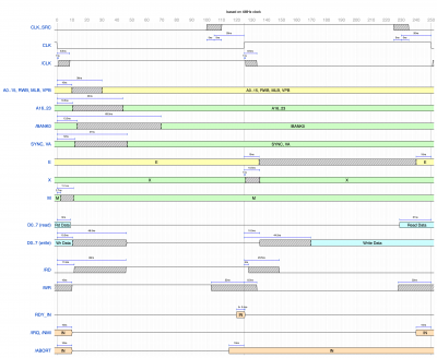
- Uses out-of-phase internal clocks to generate read and write pulses and control the data bus demultiplexing, all in accordance with proper timing (read hold time >= 10ns, write pulse time <= 10ns, bank address latch time <= 10ns but hold time >= 10ns)
- 74AHC logic used for gentle edges on the breadboard while keeping fast propagation. Faster edges (74AC, DS1035) have optional source termination.
- on top of the CPU signals are provided both positive and negative reset and clock signals, /RD and /WR pulses, VA and SYNC signals, Bank0 signal for simple memory maps
- Data bus is free when the clock is low for video access interleaving
- the RDY pin is split into an input-only RDY_IN, and output-only /WAI. RDY_IN is registered on the rising edge of the clock to ensure internal consistency
- the MX pin is split into M and X
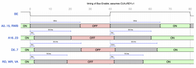
- using Bus Enable for DMA is fully supported, with the data and address buses, R/W, /RD, /WR, and VA signals being tri-stated by BE. They all have weak pull-ups/downs for default values while experimenting with BE on the breadboard.
- using RDY_IN to pause execution as if the clock were held high is fully supported for both reads and writes, with /RD and /WR being kept low and the bank address latch staying closed.

Being in spec with timings and supporting everything means the design is a bit more complicated than what you might need in your project. Presumably, you only need to build this board once to be able to re-use it in most cases. Except for anything faster than 4MHz I guess. Speed, Feature Completeness, Discrete 5V DIP ICs, choose two :mrgreen:
I suspect a future revision with a CPLD will be able to achieve more speed while keeping the features.

I would love to hear your feedback on this design, as I will be routing the PCB soon. Is there anything I missed or might want to tweak? Attached is the schematic as well as the timing diagrams.

I plan on releasing the final board as open-source, and also (maybe? full-disclosure) to sell complete kits on Tindie.

Attachment:
breakout.pdf [212.81 KiB]
Downloaded 61 times


Attachment:
breakout-bw.pdf [209.57 KiB]
Downloaded 48 times


Attachment:
Timing Main.png
Timing Main.png [ 256.7 KiB | Viewed 1137 times ]


Attachment:
Timing BE.png
Timing BE.png [ 1.05 MiB | Viewed 1137 times ]

_________________
BB816 Computer YouTube series


Top
 Profile  
Reply with quote  
PostPosted: Tue Aug 23, 2022 5:59 am 
Offline

Joined: Sun Oct 03, 2021 2:17 am
Posts: 114
Very nice, would like to play with one.


Top
 Profile  
Reply with quote  
PostPosted: Tue Aug 23, 2022 4:10 pm 
Offline
User avatar

Joined: Fri Dec 11, 2009 3:50 pm
Posts: 3346
Location: Ontario, Canada
Sorry for the slow reply, Adrien. Based on a just quick review, here are a few questions and suggestions.

Will the PCB have only one Vcc pin and one Gnd pin that insert into the breadboard? More would definitely be better! (and best to have them spread around, physically speaking -- ie; not adjacent to one another).

Next: in this section below, y' might wanna add a note to the schematic, explaining that the 74xx112, unlike most flipflops, triggers on the falling edge of its Ck input.
Attachment:
mx demux.png
mx demux.png [ 5.92 KiB | Viewed 1001 times ]


Re the reset circuit (below), I'm puzzled to see the cap between the ground and the DS1813 output. That seems iffty, because the rise time will be very slow. I know the signal gets clocked through U18, but even so... ! Certainly that cap is not what they show in the suggested application in the DS1813 data sheet, so I'm not sure what you're trying to accomplish.
Attachment:
RES circuit.png
RES circuit.png [ 6.56 KiB | Viewed 1001 times ]


Finally, and despite what the '816 data sheet may say, I'm not convinced that the '816 /RES input needs to held low for "3 clock rising edges," or even for one edge! That's based on what I recall from hands-on, stopped-clock '816 experience during this project.

My recollection may be incorrect, so if you get a minute maybe you'd like to investigate. (Do it in the name of Science!) Haha, okay, well, no pressure. But if you're curious and get a moment, on your breadboard '816 try stopping the clock while it's high. Pull /RES low then let it go high again. Then, when the clock resumes again I suspect you'll see the processor do its reset sequence. You'd also wanna try the same experiment, but stopping the clock while it's low.

-- Jeff

_________________
In 1988 my 65C02 got six new registers and 44 new full-speed instructions!
https://laughtonelectronics.com/Arcana/ ... mmary.html


Top
 Profile  
Reply with quote  
PostPosted: Tue Aug 23, 2022 6:24 pm 
Offline
User avatar

Joined: Thu May 28, 2009 9:46 pm
Posts: 8147
Location: Midwestern USA
Dr Jefyll wrote:
Finally, and despite what the '816 data sheet may say, I'm not convinced that the '816 /RES input needs to held low for "3 clock rising edges," or even for one edge! That's based on what I recall from hands-on, stopped-clock '816 experience during this project.

See here for some work I did on that.

_________________
x86?  We ain't got no x86.  We don't NEED no stinking x86!


Top
 Profile  
Reply with quote  
PostPosted: Tue Aug 23, 2022 11:19 pm 
Offline
User avatar

Joined: Sat Jul 24, 2021 1:37 pm
Posts: 282
jeffythedragonslayer wrote:
Very nice, would like to play with one.


Not making any promises about the kits, as it is a significant time investment that I can't make today, but if I see sufficient interest, I might give it a go! Thanks for your feedback.

Dr Jefyll wrote:
Sorry for the slow reply, Adrien. Based on a just quick review, here are a few questions and suggestions.

Will the PCB have only one Vcc pin and one Gnd pin that insert into the breadboard? More would definitely be better! (and best to have them spread around, physically speaking -- ie; not adjacent to one another).

Next: in this section below, y' might wanna add a note to the schematic, explaining that the 74xx112, unlike most flipflops, triggers on the falling edge of its Ck input.
Attachment:
The attachment mx demux.png is no longer available


Re the reset circuit (below), I'm puzzled to see the cap between the ground and the DS1813 output. That seems iffty, because the rise time will be very slow. I know the signal gets clocked through U18, but even so... ! Certainly that cap is not what they show in the suggested application in the DS1813 data sheet, so I'm not sure what you're trying to accomplish.
Attachment:
The attachment RES circuit.png is no longer available


Finally, and despite what the '816 data sheet may say, I'm not convinced that the '816 /RES input needs to held low for "3 clock rising edges," or even for one edge! That's based on what I recall from hands-on, stopped-clock '816 experience during this project.

My recollection may be incorrect, so if you get a minute maybe you'd like to investigate. (Do it in the name of Science!) Haha, okay, well, no pressure. But if you're curious and get a moment, on your breadboard '816 try stopping the clock while it's high. Pull /RES low then let it go high again. Then, when the clock resumes again I suspect you'll see the processor do its reset sequence. You'd also wanna try the same experiment, but stopping the clock while it's low.

-- Jeff


Really appreciate you taking the time to review the schematic.

I have made a few tweaks already since originally posting this message. Most notably I made the output connector two rows, with a full row of ground connections. The intent is to help with grounding when this is used as a mezzanine board in a larger "full" computer project. But you could certainly use it to tie a few ground wires to go around your breadboard. I will attach the updated schematic

Attachment:
breakout-bw.pdf [299.45 KiB]
Downloaded 34 times


I must admit I have no idea where I first saw someone put a cap across the reset switch, and it is one of the few things in this board I haven't studied extensively. The reason given was "to prevent spurious resets due to noise". No idea if it actually does any good or if, as you say, it may be counter-productive. The other thing I haven't studied extensively is termination, and my use of source termination resistors on fast gates to "slow down the edges" is a bit handwavy.

Finally, on the reset circuit, you're right! I just did the experiment, with CLK stopped both high and low, the CPU correctly registers the reset when the clock is restarted. Looking at my bus LEDs, it looks like the CPU changes state internally immediately. I seem to remember the 6502 needing these flip flops, and I didn't verify this on the 65816. The more you know! I think I'll keep this for "datasheet compliance" as it is not hurting anything besides board space...

BigDumbDinosaur wrote:
Dr Jefyll wrote:
Finally, and despite what the '816 data sheet may say, I'm not convinced that the '816 /RES input needs to held low for "3 clock rising edges," or even for one edge! That's based on what I recall from hands-on, stopped-clock '816 experience during this project.

See here for some work I did on that.


I'm curious about this now that I did the experiment mentioned above. Can you tell us more about your test conditions?

_________________
BB816 Computer YouTube series


Top
 Profile  
Reply with quote  
PostPosted: Fri Aug 26, 2022 5:43 pm 
Offline
User avatar

Joined: Fri Dec 11, 2009 3:50 pm
Posts: 3346
Location: Ontario, Canada
akohlbecker wrote:
I'm curious about this now that I did the experiment mentioned above. Can you tell us more about your test conditions?
I too am curious. Something must've caused the apparent contradiction. And anybody can make a mistake, I guess... it's all too easy. (can creep in because of how the information is collected and also in the process of reporting it).

-- Jeff

In the linked thread, BigDumbDinosaur wrote:
note that the 816 (and the C02) requires that reset be held low for at least two full Ø2 cycles. In monkeying around with this, I determined that failing to meet that requirement will result in the 816 not responding to the clock.

_________________
In 1988 my 65C02 got six new registers and 44 new full-speed instructions!
https://laughtonelectronics.com/Arcana/ ... mmary.html


Top
 Profile  
Reply with quote  
PostPosted: Fri Aug 26, 2022 6:08 pm 
Offline
User avatar

Joined: Thu Dec 11, 2008 1:28 pm
Posts: 10793
Location: England
What we learn from the 6502 (by way of visual6502) is that the reset input does not fixup all the state or all the t-state machinery. So, how many cycles it might take for reset to have its full effect will depend on the state of the machine - what instruction it's executing and which cycle of execution it has reached. Likewise, I think, the minimum length of time reset will be needed will depend on what the machine is doing at the time.

Edit: I suspect this will have bearing on the '816 too, which is why I mention it.

So, I'd be wary of concluding that one has measured strict limits of operation - such as a datasheet should contain - unless one has applied reset in all possible conditions.

Edit: bear in mind that at power on, the cpu will be in an indeterminate state, one which might not be reachable from any legal opcode. This too needs to result in a clean reset.


Top
 Profile  
Reply with quote  
PostPosted: Fri Aug 26, 2022 7:17 pm 
Offline
User avatar

Joined: Fri Dec 11, 2009 3:50 pm
Posts: 3346
Location: Ontario, Canada
BigEd wrote:
how many cycles it might take for reset to have its full effect will depend on the state of the machine - what instruction it's executing and which cycle of execution it has reached.
A highly pertinent comment, Ed -- thanks. The test conditions Adrien & I experienced don't cover 100% of the ground.

So, the question -- ie, will a /RES pulse lasting less than one clock reliably reset an '816? -- will remain unanswered (to my satisfaction, at least) until an exhaustive test proves "yes" or until sufficient detail is established that anyone can reproduce a failure by setting up the necessary conditions (ie, the state of the machine - what cycle of what instruction is executing, etc)

akohlbecker wrote:
Looking at my bus LEDs, it looks like the CPU changes state internally immediately.
This, to me, seems to argue for the theory that reset simply (and immediately) sets certain state bits; ie, that it is an asynchronous event, and doesn't require /RES to remain low as the result plays out. But I admit it could be both. Ie, it could begin with an asynchronous event but then also -- and only in certain conditions -- require some nailing down as the next few clock cycles elapse.

-- Jeff

_________________
In 1988 my 65C02 got six new registers and 44 new full-speed instructions!
https://laughtonelectronics.com/Arcana/ ... mmary.html


Top
 Profile  
Reply with quote  
PostPosted: Sat Aug 27, 2022 8:25 pm 
Offline

Joined: Tue Jul 05, 2005 7:08 pm
Posts: 990
Location: near Heidelberg, Germany
Doesn't RES work internally like an Interrupt sequence?
I'd be interested if a single cycle RES pulse somewhere in an IRQ sequence would actually work.

_________________
Author of the GeckOS multitasking operating system, the usb65 stack, designer of the Micro-PET and many more 6502 content: http://6502.org/users/andre/


Top
 Profile  
Reply with quote  
PostPosted: Tue Nov 01, 2022 8:40 am 
Offline
User avatar

Joined: Sat Jul 24, 2021 1:37 pm
Posts: 282
Forgot to update this thread with the final PCB!

Attachment:
Screenshot 2022-11-01 at 09.39.25.png
Screenshot 2022-11-01 at 09.39.25.png [ 1.02 MiB | Viewed 621 times ]


Attachment:
IMG_7102.jpg
IMG_7102.jpg [ 2.43 MiB | Viewed 621 times ]


I'm pretty happy with the amount of cleanup I was able to do:

Attachment:
Screenshot 2022-11-01 at 09.31.53.png
Screenshot 2022-11-01 at 09.31.53.png [ 10.06 MiB | Viewed 621 times ]


Board has been quite stable and worked the first time. I already have a few improvements I would like to make for a future version. For example, my IC sockets are too close vertically, so I can't probe the test points with my oscilloscope probes.

_________________
BB816 Computer YouTube series


Top
 Profile  
Reply with quote  
Display posts from previous:  Sort by  
Post new topic Reply to topic  [ 10 posts ] 

All times are UTC


Who is online

Users browsing this forum: Google [Bot] and 21 guests


You cannot post new topics in this forum
You cannot reply to topics in this forum
You cannot edit your posts in this forum
You cannot delete your posts in this forum
You cannot post attachments in this forum

Search for:
Jump to: