6502.org Forum  Projects  Code  Documents  Tools  Forum
It is currently Sat Apr 27, 2024 6:24 am

All times are UTC


Post new topic Reply to topic  [ 45 posts ]  Go to page 1, 2, 3  Next
Author Message
PostPosted: Mon Jul 11, 2022 8:15 am 
Offline
User avatar

Joined: Fri Nov 09, 2012 5:54 pm
Posts: 1392
Previous thread: 6525 dissection

This thread is about a transistor level dissection of the MOS 6522 VIA (Versatile Interface Adapter),
brought to you by Frank Wolf and ttlworks.
//Note, that all of the 6522 chips manufactured by MOS seem to be "revision 0".

6522 features two 8 Bit parallel I\O ports (with handshake),
two 16 Bit timers (down counters) of which one also can operate as an event counter,
plus an 8 Bit shift register for "serial communication".

6522 is "the Swiss Army knife" of IO, and it's not uncommon to have two 6522 chips in a 6502 system,
what makes the 6522 the top_selling chip in the 65xx family.

MOS 6522 (manufactured in NMOS technology) was second sourced by other companies, including Rockwell and Synertek.
We happen to know that the Rockwell 6522 had a completely different chip layout from the MOS 6522,
so it would be interesting to check whether 6522 chips from other manufacturers really are
cycle compatible to the MOS 6522 or not.

All of the 6522 NMOS variants are supposed to be out of production by now,
but WDC still manufactures the CMOS W65C22.
It would be interesting to check whether the W65C22 is cycle compatible to the MOS 6522 or not, too.

NMOS 6522 datasheets:
MOS: 6522 Versatile Interface Adapter (VIA) (Preliminary, Nov. 1977)
Rockwell: R6522 Versatile Interface Adapter (VIA) (Sep. 1993)
Synertek: SY6522 Versatile Interface Adapter (January 1978)
Synertek: SY6522 Versatile Interface Adapter (1982)
Synertek: SY6522, SY6522A VIA Programming Reference

CMOS 6522 datasheet:
WDC: W65C22 Versatile Interface Adapter (VIA) (Sep 13, 2010)

Note:
For consistence with Frank's notation, low_active signals are named foo#, not /foo.

Orientation for all the chip pictures: IRQ# pad is North.

BTW: John McMaster has microscopic pictures of the MOS 6522 silicon here.


Last edited by ttlworks on Fri Mar 10, 2023 7:43 am, edited 1 time in total.

Top
 Profile  
Reply with quote  
PostPosted: Mon Jul 11, 2022 8:16 am 
Offline
User avatar

Joined: Fri Nov 09, 2012 5:54 pm
Posts: 1392
Eagle 6.4 schematics for my schematic pictures in this thread,
just in case if somebody needs them.

Note: KiCad is supposed to be able to import these schematics,
unfortunately it doesn't seem to be possible to disable the layers 'name' and 'value' in KiCad schematics,
so making my schematics look nice and clean in KiCad will require some work, sorry.

Attachment:
6522r0_dissect_schematics.zip [699.2 KiB]
Downloaded 47 times


Top
 Profile  
Reply with quote  
PostPosted: Mon Jul 11, 2022 8:17 am 
Offline
User avatar

Joined: Fri Nov 09, 2012 5:54 pm
Posts: 1392
A picture of the MOS 6522R0 silicon, with the interesting areas marked.

Attachment:
6522r0_orientation.png
6522r0_orientation.png [ 121.78 KiB | Viewed 1537 times ]


Just as a reference, another picture of the MOS 6522R0 silicon without the markings.

Attachment:
6522r0_small.png
6522r0_small.png [ 1.1 MiB | Viewed 1537 times ]


Top
 Profile  
Reply with quote  
PostPosted: Mon Jul 11, 2022 8:19 am 
Offline
User avatar

Joined: Fri Nov 09, 2012 5:54 pm
Posts: 1392
Note, that the 6522 uses dynamic transparent latches for the counters and the shift registers.
It also uses dynamic latches for counter control and shift register control.

Everything else on the chip uses fully static transparent latches (labeled FSTL in my schematics).

6522 cheat sheet:

Attachment:
6522_0_cheatsheet.png
6522_0_cheatsheet.png [ 713.57 KiB | Viewed 1537 times ]


6522 handshake logic simplified: //omitting RST

Attachment:
6522_01_handshake.png
6522_01_handshake.png [ 117.85 KiB | Viewed 1537 times ]

That 6522 handshake logic looks a bit tricky,
I think that maybe somebody (not me) should write a technical article about it.


Top
 Profile  
Reply with quote  
PostPosted: Mon Jul 11, 2022 8:21 am 
Offline
User avatar

Joined: Fri Nov 09, 2012 5:54 pm
Posts: 1392
1) PHI //clock generator

The circuitry which generates the chip_internal (non_overlapping) PHI1 and PHI2 clock signals
from the input clock PHI0.

Nothing fancy in here, and it's "the cheap version" of the usual MOS clock generator.

Note, that some of the circuitry in the chip is clocked directly and unbuffered with PHI0.
We already had that sort of game in the 6530.

Attachment:
si6522_1_clk.png
si6522_1_clk.png [ 57.75 KiB | Viewed 1537 times ]

Attachment:
6522_1_clk.png
6522_1_clk.png [ 66.18 KiB | Viewed 1537 times ]


Top
 Profile  
Reply with quote  
PostPosted: Mon Jul 11, 2022 8:23 am 
Offline
User avatar

Joined: Fri Nov 09, 2012 5:54 pm
Posts: 1392
2a) CS //high_active chip select input

Signal from CS pad goes through an inverter,
and is sampled by a fully static transparent latch at PHI1
which emits low_active 10CS#.

Attachment:
si6522_2a_cs.png
si6522_2a_cs.png [ 18.04 KiB | Viewed 1536 times ]


;---

2b) CS# //low_active chip select input

Signal from CS# pad is samped by a fully static transparent latch at PHI1
which emits low_active 11CS#.

Attachment:
si6522_2b_ncs.png
si6522_2b_ncs.png [ 17.19 KiB | Viewed 1536 times ]


;---

2c) R/W# input //1=read, 0=write

Signal from R/W# pad goes through an inverter,
and is sampled by a fully static transparent latch at PHI1
which emits 1W/R# (0=read, 1=write).

10CS#, 11CS#, W/R# go into "18) bus control, handshake logic".

Attachment:
si6522_2c_rw.png
si6522_2c_rw.png [ 20.71 KiB | Viewed 1536 times ]


;---

2d) IRQ# output

IRQ# pad is the low_active interrupt output of the 6522,
pulled to GND by an "open collector" inverter,
which is fed by high_active IRQ.

Note, that the 6522 has no pullup resistor on chip,
so an external pullup resistor is supposed to be placed between IRQ# and VCC.

IRQ is generated in "12) IFR". //interrupt flag register.

Attachment:
si6522_2d_irq.png
si6522_2d_irq.png [ 39.25 KiB | Viewed 1536 times ]


;---

2e) RST# input //low_active hardware reset

RST basically goes through an inverter, and becomes the high_active RST signal.

Note, that like in the 6530, the 6522 hardware reset is not synchronized with any clock.
It's an asynchronous signal.

Attachment:
si6522_2e_rst.png
si6522_2e_rst.png [ 26.21 KiB | Viewed 1536 times ]


;---

Now for the schematics related to all of the pads:

Attachment:
6522_2_some_pads.png
6522_2_some_pads.png [ 127.15 KiB | Viewed 1536 times ]


Top
 Profile  
Reply with quote  
PostPosted: Mon Jul 11, 2022 8:25 am 
Offline
User avatar

Joined: Fri Nov 09, 2012 5:54 pm
Posts: 1392
3) A0 input

A0..A3 pads connect to the external address bus.

Chip layout for the A0..A3 circuitry looks pretty similar, so we just focus on A0.

Basically, the signal from the A0 pad is sampled by a fully static transparent latch at PHI1,
which emits the buffered signals 1A0 (high_active) and 1A0# (low_active).

1A0 and 1A0# are sampled by another fully static transparent latch at PHI0,
which emits 0A0 (high_active) and 0A0# (low_active).

The outputs of these latches go into "8) address decoder",
where they are used for selecting the register to be read/written.

Attachment:
si6522_3_a0.png
si6522_3_a0.png [ 29.3 KiB | Viewed 1536 times ]

Attachment:
6522_3_a0.png
6522_3_a0.png [ 75.82 KiB | Viewed 1536 times ]


Top
 Profile  
Reply with quote  
PostPosted: Mon Jul 11, 2022 8:26 am 
Offline
User avatar

Joined: Fri Nov 09, 2012 5:54 pm
Posts: 1392
4) D0 input/output

D0..D7 pads connect to the external data bus.

Chip layout for the D0..D7 circuitry looks pretty identical,
so we just focus on D0.

;---

On the output side, basically we have a non_inverting push/pull driver,
fed by the internal read data bus signal D0r.
If the low_active output enable signal OE_RD# is low,
the driver puts D0r on the D0 pad, and that's all there is to it.

OE_RD# is generated in "18) bus control, handshake".
OE_RD# is active during PHI0, when the 6502 reads a 6522 register.

Note, that we have precharge FETs which pull D0..7r to VCC during PHI1.
See "17) D0..7w inverters, precharge".

;---

On the input side, we have a fully transparent static latch
which samples the D0 pad during PHI0.

The output of the flipflop goes through a driver which feeds
the low_active D0w# internal write data bus line.

Note, that the driver has no output enable,
and that the way how the driver is attached to the latch makes sure
that the FETs in the driver do non_overlapping switching to GND/VCC.

Also note, that we have 8 inverting super buffers which turn D0..7w# (low_active)
into D0..7w (high_active), see "17) D0..7w# inverters, precharge".
They are ocated between the D2..5 pads and "16c) Timer 1 low" on the chip.

;---

Attachment:
si6522_4_d0.png
si6522_4_d0.png [ 37.97 KiB | Viewed 1536 times ]

Attachment:
6522_4_d0.png
6522_4_d0.png [ 97.96 KiB | Viewed 1536 times ]


Top
 Profile  
Reply with quote  
PostPosted: Mon Jul 11, 2022 8:27 am 
Offline
User avatar

Joined: Fri Nov 09, 2012 5:54 pm
Posts: 1392
5) PA0

PA0..7 is an 8 Bit I\O port.

Chip layout for PA0..7 is pretty identical,
so we just focus on PA0.

;---

On the output side, we have a non_inverting super buffer,
fed by the low_active PA0# signal.
The buffer drives a big FET which switches PA0 to GND,
also there is a ca. 2.25 kOhm pullup between PA0 and VCC.

PA0# high switches PA0 to GND.

PA0# is generated in "7) PA,PB registers".

//Chip layout related to the pullup makes creative use of space.

;---

On the input side, we have a fully static transparent latch which samples PA0
when high_active control signal LD_PA is high.

The latch has a low_active output named PA0i#.
PA0i# goes into "7) PA,PB registers".

LD_PA is generated by a NAND, which is located in "8c) PA input latch control".
The inputs of the NAND are fed by ACR0 and IFR1:
If PA latching is disabled by ACR0=0, PA input latches always are transparent.
If PA latching is enabled by ACR0=1, IFR1=1 freezes the PA input latches.

//IFR1 interrupt flag is set by active CA1 input edge.

;---

Attachment:
si6522_5_pa0.png
si6522_5_pa0.png [ 46.72 KiB | Viewed 1536 times ]

Attachment:
6522_5_pa0.png
6522_5_pa0.png [ 60.1 KiB | Viewed 1536 times ]


Top
 Profile  
Reply with quote  
PostPosted: Mon Jul 11, 2022 8:29 am 
Offline
User avatar

Joined: Fri Nov 09, 2012 5:54 pm
Posts: 1392
6a) PB0

PB0..7 is another 8 Bit I\O port.

Chip layout for PB0..6 is pretty identical,
so we just focus on PB0.

;---

On the output side, wa have a non_inverting push/pull driver,
fed by the high_active PB0o signal, which switches the PB0 pad to GND/VCC.

If the high_active PB0_DIR signal is high, this enables the driver.

A ca. 5 kOhm pullup ties the PB0 pad to VCC.

PB0o and PB0_DIR are generated in "7) PA,PB registers".

;---

On the input side, we have a fully static transparent latch which samples PB0
when high_active control signal LD_PB is high.

A 2:1 multiplexer controlled by PB_DIR either routes
the output of the latch (if PB0_DIR=0, PB0 direction is input)
or the PB0o signal (if PB0_DIR=1, PB0 direction is output)
into an inverter which emits the low_active PB0i# signal.

Background is, that if the PB0 output driver has to sink/source a lot of current,
we can't be sure if the voltage at the output of said driver matches high or low level.
So if PB0 direction is output, the 6502 reads what's in the register which feeds
the PB0 output driver input instead of what's on the output driver output,#
just to be on the safe side during read/modify/write operations and such.

PB0i# goes into "7) PA,PB registers".

Note, that Timer 2 can count falling edges on PB6.
The input of "21) PB6 falling edge detector" taps into the PB6# signal,
which is generated by an inverter from the PB6 pad.
//Said inverter belongs to the PB6 input latch.

LD_PB is generated by a NAND, which is located in "8d) PB input latch control".
The inputs of the NAND are fed by ACR1 and by the output of a transparent latch
which samples IFR4 during PHI1:
If PB latching is disabled by ACR1=0, PB input latches always are transparent.
If PB latching is enabled by ACR1=1, IFR4=1 (sampled during PHI1) freezes the PB input latches.

//IFR4 interrupt flag is set by active CB1 input edge.

;---

Attachment:
si6522_6a_pb0.png
si6522_6a_pb0.png [ 40.39 KiB | Viewed 1536 times ]

Attachment:
6522_6a_pb0.png
6522_6a_pb0.png [ 93.5 KiB | Viewed 1536 times ]


Top
 Profile  
Reply with quote  
PostPosted: Mon Jul 11, 2022 8:30 am 
Offline
User avatar

Joined: Fri Nov 09, 2012 5:54 pm
Posts: 1392
6b) PB7

PB7 pad input\output circuitry is based on what we had in "6a) PB0",
but because Timer 1 can generate an output signal on PB7,
we have a little bit of additional circuitry on the output side.

If ACR7=0, Timer 1 makes not use of PB7, and the game goes like with "6a) PB0".

If ACR7=1, Timer 1 makes use of PB7, overriding the signals PB7o and PB7_DIR.
The PB7 output driver is enabled.
The PB7 output driver is fed by signal PB7_T1 instead of PB7o.
The inverter emitting PB7i# is fed by PB7_T1 instead of PB7o.
//PB7o and PB7_DIR are just getting ignored by ACR7=1, not changed.

The Timer 1 output signal PB7_T1 is generated in "16b) T1H control".


Note, that I'm trying to simplify things in the description,
because on the silicon, the PB0..PB6 circuitry uses a high_active PB0..6o signal,
but the PB7 circuitry uses a low_active PB7o# signal.

Attachment:
si6522_6b_pb7.png
si6522_6b_pb7.png [ 68.41 KiB | Viewed 1536 times ]

Attachment:
6522_6b_pb7.png
6522_6b_pb7.png [ 117.57 KiB | Viewed 1536 times ]


Top
 Profile  
Reply with quote  
PostPosted: Mon Jul 11, 2022 8:34 am 
Offline
User avatar

Joined: Fri Nov 09, 2012 5:54 pm
Posts: 1392
7a) PA,PB registers

It looks pretty similar to what we already had in the 6530.

RST active asynchronously clears all of the Bits in the registers
ORA, ORB, DDRA, DDRB.

Register section for PA0..PA7 looks pretty identical,
register section for PB0..PB6 looks pretty identical,
so we just focus on the circuitry for the PA0 and PB0 registers.

PB7 register circuitry is just a variation of PB0..6 register circuitry,
emitting a low_active PB7o# signal instead of a high_active PB7o signal.

;---

IRA: PA data input register

High_active control signal R_IRA connects/switches the output of an inverter
to the D0r internal data bus signal during PHI1=0 (wich is different from PHI2=1).
The inverter is fed with the PA0i# signal generated in "5) PA0",
and that's all there is to it.

;---

ORA: PA data output register

We have a fully static RS flipflop working as the ORA0 register Bit.
The internal write data bus signals D0w (high_active) and D0w# (low_active)
are used to set/clear the register Bit by high active control signal W_ORA during PHI0=0.

A NOR gate fed by ORA0 and DDRA0# generates PA0o#.
;
If data register ORA=0, and PA direction is set as output by DDRA0=1,
PA0o# is high, so the output driver switches PA0 to GND.

;---

DDRA: PA direction register //0=input, 1=output

We have a fully static RS flipflop working as the DDRA register Bit.
The internal write data bus signals D0w (high_active) and D0w# (low_active)
are used to set/clear the register Bit by high active control signal W_DDRA during PHI0=0.

High_active read control signal R_DDRA connects/switches the output of the RS flipflop
to the internal D0r read data bus line during PHI1=0.

;===

IRB: PB data input register

High_active control signal R_IRB connects/switches the output of an inverter
to the D0r internal data bus signal during PHI1=0 (wich is different from PHI2=1).
The inverter is fed with the PB0i# signal generated in "6a) PB0",
and that's all there is to it.

;---

ORB PB data output register

We have a fully static RS flipflop working as the ORB0 register Bit.
The internal write data bus signals D0w (high_active) and D0w# (low_active)
are used to set/clear the register Bit by high active control signal W_ORB during PHI0=0.

The buffered output of the RS flipflop is PB0o.

;---

DDRB: PB direction register //0=input, 1=output

We have a fully static RS flipflop working as the DDRB register Bit.
The internal write data bus signals D0w (high_active) and D0w# (low_active)
are used to set/clear the register Bit by high active control signal W_DDRB during PHI0=0.

The buffered output of the RS flipflop is PB0_DIR.

High_active read control signal R_DDRB connects/switches the buffered output of the RS flipflop
to the internal D0r read data bus line during PHI1=0.

;===

Of course I'm simplifying things, because the RS flipflops are not built from two NOR gates,
they are built from two "open collector" inverters which have pullups to VCC at the outputs.
This trick makes the RS flipflops smaller than when using NOR gates.
For RS flipflops built like this, R# is identical to Q, and S# is identical to Q#.

Read/write control signals enter the register block from the South.
North from the register block, we have FETs controlled by the clock signals,
switching the other end of every control signal to GND in the right moment,
to make sure that the control signals are inactive when they are supposed to be.

For every register in the 6522 it's implemented like this,
and we have seen that trick quite often in other MOS 65xx peripheral chips.

Attachment:
si6522_7_pa_pb_regs.png
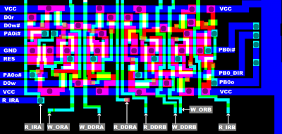
si6522_7_pa_pb_regs.png [ 59.22 KiB | Viewed 1535 times ]

Attachment:
si6522_7_pa_pb_regs_north.png
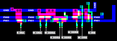
si6522_7_pa_pb_regs_north.png [ 21.41 KiB | Viewed 1535 times ]

Attachment:
si6522_7_pb7_reg.png
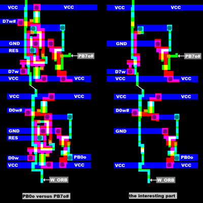
si6522_7_pb7_reg.png [ 34.7 KiB | Viewed 1535 times ]

Attachment:
6522_7_pa_pb_regs.png
6522_7_pa_pb_regs.png [ 155.35 KiB | Viewed 1535 times ]


;---

Like in the 6530, when the 6502 reads data from the I\O ports,
it reads directly what's on the PA0..7 and PB0..7 pads.

To be more specific:
If PA\PB are configurated as inputs, and if PA\PB latching is disabled, the 6502 "directly" reads what's on the PA\PB pads.
In this case: if there is a spike on the PA\PB inputs during PHI2 while the 6502 is reading the PA\PB data input registers,
said spike is supposed to show up on the 6502 data bus during PHI2, and that's not good for signal integrity.

Maybe it would be better for signal integrity to sample the inputs from the pads
by transparent latches during PHI1=1, but then you need to make sure that the
"PA input latch" and "PB input latch" circuitry stays somewhat cycle/timing compatible to the original.


Last edited by ttlworks on Mon Jul 11, 2022 11:56 am, edited 1 time in total.

Top
 Profile  
Reply with quote  
PostPosted: Mon Jul 11, 2022 8:37 am 
Offline
User avatar

Joined: Fri Nov 09, 2012 5:54 pm
Posts: 1392
8) address decoder

The part that generates all of the register read/write control signals
during a certain clock phase, and it's quite big.
So I had to break it into three parts.

In the 6530, the address decoder is a PLA.
In the 6522, the address decoder is built from conventional logic gates.

;---

For read control signals, A0..3 pads are sampled by transparent latches during PHI1=1,
which emit the high_active 1A0..3 and the low_active 1A0..3# address signals, see "3) A0",
for selecting a 6522 register to be read.
;
Read control signals go active during PHI1=0,
that's the second half of the bus cycle in which the 6502 reads a 6522 register.

For write control signals, 1A0..3 (and 1A0..3#) are sampled by transparent latches during PHI0=1,
which emit the high_active 0A0..3 and the low_active 0A0..3# address signals, see "3) A0",
for selecting a 6522 register to be written.
;
Write control signals go active during PHI0=0,
that's the first half of the bus cycle _after_ a 6502 write cycle.

WE# is a low_active signal which is generated in "18) bus control, handshake logic".
It is active when the 6502 does a 6522 register write.

;---

Some little peculiarities in the circuitry related to handshake, Timer reads/writes, and IER writes.

Also we have some circuitry in the address decoder area which is not directly related to address decoding,
like some part of the Timer 1/2 carry circuitry, some part of Timer 2 control (T2H_LD and T2H_CNT),
and PA input latch control.
We are getting there later.

;---

$0 read IRB (input register PB), write ORB (output register PB)
$1 read IRA (input register PA) with handshake, write ORA (output register A) with handshake
$2 DDRB (data direction register PB) //0=input, 1=output
$3 DDRA (data direction register PA) //0=input, 1=output

$4 read T1L counter, write T1L latch
$5 read T1H counter, write T1H latch+counter
$6 T1L latch
$7 T1H latch
$8 read T2L, write T2L latch
$9 T2H counter

$A SR (shift register)
$B ACR (auxiliary control register)
$C PCR (peripheral control register)
$D IFR (interrupt flag register)
$E IER (interrupt enable register)
$F read IRA (input register PA) without handshake, write ORA (output register A) without handshake

;---

Attachment:
si6522_8a_address_decoder.png
si6522_8a_address_decoder.png [ 73.2 KiB | Viewed 1535 times ]

Attachment:
6522_8a_address_decoder.png
6522_8a_address_decoder.png [ 136.63 KiB | Viewed 1535 times ]


Attachment:
si6522_8b_address_decoder.png
si6522_8b_address_decoder.png [ 92.51 KiB | Viewed 1535 times ]

Attachment:
6522_8b_address_decoder.png
6522_8b_address_decoder.png [ 190.02 KiB | Viewed 1535 times ]


Attachment:
si6522_8c_address_decoder.png
si6522_8c_address_decoder.png [ 147.19 KiB | Viewed 1535 times ]

Attachment:
6522_8c_address_decoder.png
6522_8c_address_decoder.png [ 292.03 KiB | Viewed 1535 times ]


;---

Attachment:
6522_8_address_decoder.png
6522_8_address_decoder.png [ 140.55 KiB | Viewed 1535 times ]


Last edited by ttlworks on Mon Jul 11, 2022 11:23 am, edited 1 time in total.

Top
 Profile  
Reply with quote  
PostPosted: Mon Jul 11, 2022 8:40 am 
Offline
User avatar

Joined: Fri Nov 09, 2012 5:54 pm
Posts: 1392
9) ACR,PCR registers

Not much to say, these registers are built in the same way as the DDRB register:
Every register Bit is a static RS flipflop, flipflops are set/cleared by the internal data write busses
D0..7w and D0..7w# by a high_active write control signal during PHI0=0.

The buffered outputs of the RS flipflops goes somewhere to control logic on the chip,
also switches controlled by a high_active read control signal place the output of a register
on the internal read data bus D0..7r during PHI1=0.

Note, that all of the register Bits are asynchronously cleared when RST is active.

Like with the PA,PB register block, read/write control signals enter the ACR,PCR register block from the South,
and at the North of the ACR,PCR register block we have switches which make sure that these control signals
are inactive during a certain clock phase.

Of course I'm simplifying things, because the RS flipflops are not built from two NOR gates,
they are built from two "open collector" inverters which have pullups to VCC at the outputs.
This trick makes the RS flipflops smaller than when using NOR gates.
For RS flipflops built like this, R# is identical to Q, and S# is identical to Q#.

;---

ACR: Auxiliary Control Register

ACR7..6: Timer 1 control
ACR5: Timer 2 control //0=count down with PHI2, 1=count down one step after PB6 falling edge
ACR4..2: shift register control
ACR1: PB latch //1=enabled, 0=disabled
ACR0: PA latch //1=enabled, 0=disabled

;...

ACR4..2: shift register control
000: disabled
001: shift in under control of Timer 2
010: shift in under control of PHI2
011: shift in under control of external clock
100: shift out free running at Timer 2 rate
101: shift out under control of Timer 2
110: shift out under control of PHI2
111: shift out under control of external clock

//Note: shift out means circular shift register operation.

;---

PCR: Peripheral Control Register

PCR7..5: CB2 control
PCR4: CB1 control //0=falling edge, 1=rising edge
PCR3..1: CA2 control
PCR0: CA1 control //0=falling edge, 1=rising edge

;...

PCR7..5 CB2 control, PCR3..1 CA3 control:
000: input falling edge
001: independent interrupt input falling edge
010: input rising edge
011: independent interrupt input rising edge
100: handshake output
101: pulse output
110: LOW output
111: HIGH output

;---

Attachment:
si6522_9_acr_pcr.png
si6522_9_acr_pcr.png [ 16.79 KiB | Viewed 1535 times ]

Attachment:
si6522_acr_pcr_north.png
si6522_acr_pcr_north.png [ 10.91 KiB | Viewed 1535 times ]

Attachment:
6522_9_acr_pcr_regs.png
6522_9_acr_pcr_regs.png [ 97.1 KiB | Viewed 1535 times ]


Top
 Profile  
Reply with quote  
PostPosted: Mon Jul 11, 2022 8:41 am 
Offline
User avatar

Joined: Fri Nov 09, 2012 5:54 pm
Posts: 1392
10) shift register

8 Bit shift register, which shifts out MSB (that's a binary "shift left").

It uses dynamic transparent latches during the shift phase,
and half_static transparent latches during hold phase.
Output of shift register Bit 7 (MSB) is labeled SR_out7.

Note, that SR_out7 goes into a latch at the output of the shift register:
one switch of the latch is part of the shift register block (it's easy to miss that),
the rest of the latch is located in "22) shift register control".

The output SR_CB2_Q of said latch goes to "19) CB2".
If the shift register shifts out (ACR4=1), the CB2 output driver is fed with SR_CB2_Q.
CB2 is the data input/output of the shift register.

In "22) shift register control", we have a 2:1 multiplexer controlled by ACR4.
The output of said multiplexer goes into the LSB of the shift register as SR_IN.
If the shift register shifts in (ACR4=0), the signal from the CB2 pad goes into the LSB.
If the shift register shifts out (ACR4=1), the signal SR_CB2_Q goes into the LSB,
means if the shift register shifts out it does circular shift.

CB1 is the clock input/output for the shift register.
Depending on tha ACR4..2 shift register configuration Bits described in "9) ACR,PCR registers",
CB1 either is fed by an external clock, or emits a clock signal generated by "22) shift register control".
In both cases, an edge detector in "20) CB1" senses the CB1 pad, reports an active edge back to
some circuitry in "22) shift register control" which then generates the clock signals
for shifting/counting the Bits.

Means in "22) shift register control", we have a clock generator for generating the CB1 clock,
we have another clock generator for generating the shift register\Bit counter clocks,
and the generators are "a different pair of shoes".

Note, that the CB1 edge detector related to the shift register senses
CB1 falling edge for shift in, and CB1 rising edge for shift out.

;---

Now for the shift register control signals:

W_SR (high_active) writes the shift register from the internal write data bus D0..7w during PHI0=0.
R_SR (high_active) reads the shift register into the internal read data bus D0..7r during PHI1=0.
These two signals are generated in "8) address decoder", and they also go into "22) shift register control".

The rest of the shift register control signals in generated in "22) shift register control":
HOLD_SR (high_active) clock signal just makes the shift register hold/refresh the current data.
SHIFT_SR (high_active) clock signal shifts the Bits by one step.

North of the shift register block, we have the usual FETs switching the control signals to GND
during a certain clock phase.

Attachment:
si6522_10_sr.png
si6522_10_sr.png [ 15.45 KiB | Viewed 1534 times ]

Attachment:
si6522_10_sr_north.png
si6522_10_sr_north.png [ 13.16 KiB | Viewed 1534 times ]

Attachment:
6522_10_sr.png
6522_10_sr.png [ 71.98 KiB | Viewed 1534 times ]


Top
 Profile  
Reply with quote  
Display posts from previous:  Sort by  
Post new topic Reply to topic  [ 45 posts ]  Go to page 1, 2, 3  Next

All times are UTC


Who is online

Users browsing this forum: No registered users and 31 guests


You cannot post new topics in this forum
You cannot reply to topics in this forum
You cannot edit your posts in this forum
You cannot delete your posts in this forum
You cannot post attachments in this forum

Search for:
Jump to: