6502.org Forum  Projects  Code  Documents  Tools  Forum
It is currently Sun May 05, 2024 4:18 am

All times are UTC


Post new topic Reply to topic  [ 10 posts ] 
Author Message
PostPosted: Thu Apr 21, 2022 9:21 pm 
Offline
User avatar

Joined: Mon May 25, 2015 2:25 pm
Posts: 632
Location: Gillies, Ontario, Canada
I have been working on my Vulcan-74 project (final version) on weekends and have it mostly ready to document.
The last part to optimize was the 6502 IO section, as my old system only ran the CPU at 10MHz.

I did manage to get 14.318MHz several times, but after the IO decoding was added, it became a bit unstable.
So.... I learned a few new tricks!

First, have a look at this...

Image

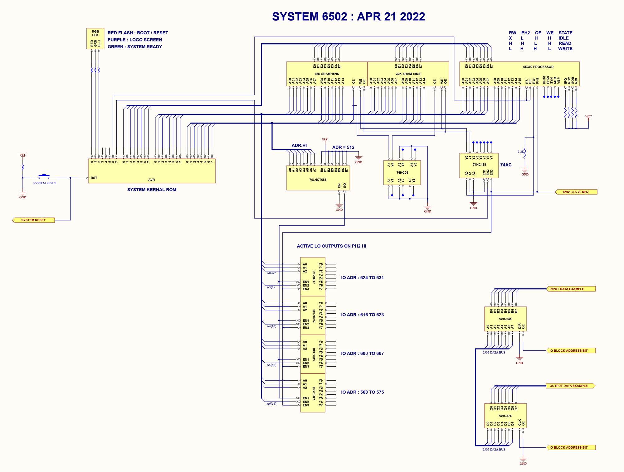
I used to gate RW and PH2 using the usual NAND schematic that seems to be the accepted standard. This works well, and only adds the propagation delay of 2 NAND gates at most, so let's just say it has about 16 nanoseconds of delay.

I wasn't satisfied with that, so I tried a ton of different schemes to finally come up with the one shown above that only introduces 4 nanoseconds total!
This is of course using AC logic, but even with plan old HC (8 ns delay) logic, 18 MHz was stable.

The secret sauce : using a single 138 as the RW/PH2 gating.

I call this setup stable at 20MHz because it will actually do 25MHz, and breaks down around 28MHz. This is my margin of safety.
My IO decode logic is also greatly simplified, feeding the address and select line of the four 138s directly form the lower address bus after triggering the chain from the higher bus at address 512. This is working perfectly on my massive board, and the 65C02 is a real performer now!

Also not that this is the WesternDesgin 65C02, not the TTL version, and I am running fully from 15ns SRAM that has been boot loaded with my Kernal.
A system kludged down with ancient ROM would probably never achieve this level of speed without some serious variable clocking magic.

I am also using my slowest (15ns) SRAM with an inverter to tie the 32K together. I bet 25 MHz or better is possible with 10ns SRAM!

That's it for now, just wanted to share my discovery.... 20MHz 6502 Baby!

Will post some eye candy soon, Vulcan-74 is now 100% logic based and pushing our 360x240 NTSC with 16384 colors.
Blitter performance is just smokin' fast now (10 million pixels per second on a 16 bit video databus!), I am kind of laughing at my previous works now.

Later!
Brad


Top
 Profile  
Reply with quote  
PostPosted: Thu Apr 21, 2022 11:36 pm 
Offline
User avatar

Joined: Thu May 28, 2009 9:46 pm
Posts: 8173
Location: Midwestern USA
I’m not able to read the entire schematic, but I can make out two things that might warrant review.

74HC logic is likely too slow for reliable operation above 10 MHz. I use 74AC logic in my POC units. POC V1.3 runs at 16 MHz, and its predecessor runs at 20 MHz. 74AHC performs at the same level as 74AC, but with less-aggressive outputs.

Chip selects should not be qualified by Ø2. Doing to significantly shrinks the the timing window from when the address bus becomes stable (about midway through Ø2 low) until the selected device is ready for access. Best performance is achieved by allowing selection to occur during Ø2 low and using Ø2 to qualify read/write operations, especially writes.

_________________
x86?  We ain't got no x86.  We don't NEED no stinking x86!


Top
 Profile  
Reply with quote  
PostPosted: Thu Apr 21, 2022 11:38 pm 
Offline
User avatar

Joined: Mon May 25, 2015 2:25 pm
Posts: 632
Location: Gillies, Ontario, Canada
Here is the basic RW + PH2 Qualifier with the other stuff removed.
I have had this running @20MHz for several weeks, using the entire 64K SRAM without any glitches.

Attachment:
RWQ.png
RWQ.png [ 30.35 KiB | Viewed 781 times ]


Cheers,
Brad


Top
 Profile  
Reply with quote  
PostPosted: Thu Apr 21, 2022 11:43 pm 
Offline
User avatar

Joined: Mon May 25, 2015 2:25 pm
Posts: 632
Location: Gillies, Ontario, Canada
Just right click and open in a new window.
Yes, HC offers only 14MHz operation on my board.
With the AC, I can do 25, which is why I consider 20 to be "safe".

I will have to think about your statement, but unless I am missing something, my circuit does exactly what this does, minus the extra gate delay...

Attachment:
RW Connection to RAM.gif
RW Connection to RAM.gif [ 19.57 KiB | Viewed 781 times ]


Also the same as this simpler version (used to use this)...

Attachment:
oe_rw.gif
oe_rw.gif [ 5.1 KiB | Viewed 781 times ]


Also, I never use CE on SRAM. In fact, you can do away with OE in some cases as long as you have a bidirectional buffer.

Ps...
What browser are you using? There should be scroll bars to allow moving around the large image.

Thanks,
Brad

BigDumbDinosaur wrote:
I’m not able to read the entire schematic, but I can make out two things that might warrant review.

74HC logic is likely too slow for reliable operation above 10 MHz. I use 74AC logic in my POC units. POC V1.3 runs at 16 MHz, and its predecessor runs at 20 MHz. 74AHC performs at the same level as 74AC, but with less-aggressive outputs.

Chip selects should not be qualified by Ø2. Doing to significantly shrinks the the timing window from when the address bus becomes stable (about midway through Ø2 low) until the selected device is ready for access. Best performance is achieved by allowing selection to occur during Ø2 low and using Ø2 to qualify read/write operations, especially writes.


Top
 Profile  
Reply with quote  
PostPosted: Fri Apr 22, 2022 12:09 am 
Offline
User avatar

Joined: Mon May 25, 2015 2:25 pm
Posts: 632
Location: Gillies, Ontario, Canada
Here is the board that my 20MHz 6502 has been powering for almost a month now.
I leave this running in my lab to motivate myself to finish the project.

Attachment:
tn.jpg
tn.jpg [ 53.18 KiB | Viewed 768 times ]


https://www.youtube.com/watch?v=OxsC8UrLEuM


That image is 360x240 with 16K colors. Yep, NTSC with 16.384 color on screen at once!
The blitter is hardly working here, and will be doing a lot more once I get the storage system done.

This is just a rough test, which is why the wiring is so ugly. I am redoing it completely once more for my blog before hand wiring it all.
The 64 wires shown at the top are the taps I made using 74HC245 gates to get 64 evenly spaced propagation delays of 3.8 nanoseconds.
Generating NTSC color like this is so much more challenging than going VGA, which is why I decided to go fully retro this time.
My first Vulcan-74 prototype was VGA and it didn't feel old-school enough!

All parts on the board : one 6502, some SRAM, and all 1980's era logic.

Brad


Last edited by Oneironaut on Fri Apr 22, 2022 1:35 am, edited 5 times in total.

Top
 Profile  
Reply with quote  
PostPosted: Fri Apr 22, 2022 12:10 am 
Offline
User avatar

Joined: Thu May 28, 2009 9:46 pm
Posts: 8173
Location: Midwestern USA
Oneironaut wrote:
Just right click and open in a new window.

Some pieces seem to be missing from the schematic. Is it in color?

Quote:
I will have to think about your statement, but unless I am missing something, my circuit does exactly what this does, minus the extra gate delay...

What extra gate delay? On the WDC 65C02, RWB is valid well before the rise of Ø2. So the inverter’s output will already be reflecting the state of RWB when Ø2 goes high, which means there is effectively a single gate delay.

You should know that I have a derivative of that circuit that works at 50 MHz in a test rig, 50 being the highest frequency for which I have an oscillator in my parts pile. Here's the derivative, which is a single-chip solution:

Attachment:
File comment: Single-Chip Qualified Read/Write
read_write_qualify_alt.gif
read_write_qualify_alt.gif [ 46.98 KiB | Viewed 775 times ]

Quote:
Also, I never use CE on SRAM. In fact, you can do away with OE in some cases as long as you have a bidirectional buffer.

With most SRAMs, the time from when /OE is asserted until data is emitted is always shorter than the time from when /CE is asserted. Cypress, in particular, recommends /CE be asserted as soon as a valid address appears and that output be gated with only with /OE. Their timing diagrams clearly illustrate that asserting /CE before /OE will produce faster response.

_________________
x86?  We ain't got no x86.  We don't NEED no stinking x86!


Top
 Profile  
Reply with quote  
PostPosted: Fri Apr 22, 2022 12:38 am 
Offline
User avatar

Joined: Mon May 25, 2015 2:25 pm
Posts: 632
Location: Gillies, Ontario, Canada
In that case dude, your Jedi skills are at a level I can only dream of.
I thought I was doin' good with a 6502 at 20MHz!

Please post a schematic (with RAM), I would love to see my system push 50Mhz!
Even using an FPGA with very tightly controlled delays, I could not get 50MHz out of a 10ns SRAM.

For now though, I shall continue with my 138 solution, which so far has yielded my best performance, even when put up against the other 2 solutions shown above.
I do want to know more about your 50MHz rig though!

Brad

BigDumbDinosaur wrote:
You should know that I have a derivative of that circuit that works at 50 MHz in a test rig, 50 being the highest frequency for which I have an oscillator in my parts pile. Here's the derivative, which is a single-chip solution:


Top
 Profile  
Reply with quote  
PostPosted: Fri Apr 22, 2022 6:32 am 
Offline
User avatar

Joined: Thu May 28, 2009 9:46 pm
Posts: 8173
Location: Midwestern USA
Oneironaut wrote:
In that case dude, your Jedi skills are at a level I can only dream of.
I thought I was doin' good with a 6502 at 20MHz!

:lol: :lol: :lol:

You misunderstood me. I tested the read/write circuit at 50 Mhz, observing its behavior on the scope. No microprocessors were involved.

My POC V1.2 unit runs at 20 MHz. POC V1.3, the current unit, is stable at 16 MHz. Due to prop time associated with bank latching and its effect on the clock-stretching circuit that wait-states ROM and I/O, things go off the rails around 18 MHz. The next rendition will use a CPLD to handle glue logic and latch the bank bits, which should improve the timing picture.

_________________
x86?  We ain't got no x86.  We don't NEED no stinking x86!


Top
 Profile  
Reply with quote  
PostPosted: Fri Apr 22, 2022 12:48 pm 
Offline
User avatar

Joined: Mon May 25, 2015 2:25 pm
Posts: 632
Location: Gillies, Ontario, Canada
Ah... got it. At least it kept me up late thinking about how it was possible.
I had visions of liquid nitrogen, sub nanosecond clock phase tweaking, and overvolting to double digits!

I guess our timing circuits are really dependent on our designs. With mine, I latch out about 30 8 bit values to various 574s on my board, and read 4 values provided by the 245s. Each of those is enabled by the outputs on my 138 decoders. I found that with the AC138 gating RW/PH2, I only required HC138s in my decode.

I checked again, and my system runs fine 1t 25 MHz, breaking down around 28 MHz.
So 20 MHz seems to be the magic number in my design.

In one past experiment, I also drove PH2 at 25 MHz from an FPGA, splitting the HI phase to be about 75% longer than the LO phase. This was stable, but highly complex.
I used the FPGA block RAM as well, so we can say that it was about 6ns access time.

Since I only hoped for 10 MHz speed on this project, I am going to consider 20 MHz a total win.
I am now working on the second massive breadboard, which contains the 6 channel sound system.
This is another 364 square inch breadboard with 250+ ICs, and it has its own 6502 to handle the phase accumulator and channel commands.

Cheers,
Brad

BigDumbDinosaur wrote:
Oneironaut wrote:
In that case dude, your Jedi skills are at a level I can only dream of.
I thought I was doin' good with a 6502 at 20MHz!

:lol: :lol: :lol:

You misunderstood me. I tested the read/write circuit at 50 Mhz, observing its behavior on the scope. No microprocessors were involved.

My POC V1.2 unit runs at 20 MHz. POC V1.3, the current unit, is stable at 16 MHz. Due to prop time associated with bank latching and its effect on the clock-stretching circuit that wait-states ROM and I/O, things go off the rails around 18 MHz. The next rendition will use a CPLD to handle glue logic and latch the bank bits, which should improve the timing picture.


Top
 Profile  
Reply with quote  
PostPosted: Thu May 26, 2022 11:53 am 
Offline
User avatar

Joined: Tue Aug 11, 2020 3:45 am
Posts: 311
Location: A magnetic field
I like to be wowwed and you never disappoint. 20MHz is becoming routine. However, 20MHz, 64KB RAM *and* 32 I/O strobes is very impressive.

Your work often leads to disbelief but I never doubt your figures. Actually, you've inspired me to adapt your address decode strategy. It is possible to eliminate the 74x688 and make one tier of address decode (and extended address latching) which all runs in parallel.

I am alarmed by your lack of capacitors but you can't argue with success.

BigDumbDinosaur on Fri 22 Apr 2022 wrote:
I tested the read/write circuit at 50 Mhz, observing its behavior on the scope.


On Tue 22 Mar 2022, I confirmed that 74HC138 and 74HC139 inverts a 64MHz crystal and implements BigDumbDinosaur's suggested circuit without encountering latency from two sets of clamp diodes. Actually, I ordered 64MHz, 72MHz and 80MHz crystals from dubious suppliers. Of these, one arrived and claims to be 64.000MHz crystal. From data-sheet inferences and cursory test in a limited temperature range, a system with 30MHz RAM and eight or more I/O strobes is possible. With clock stretching, asymmetric clock and 74AC logic, 40MHz might be possible.

74HC139 has become relatively scarce but I only considered 74x00 as a substitute rather than 74x138. Radical Brad shows empirically that 74x138 works for read/write qualification at 20MHz.

Regarding asymmetric clock, akohlbecker has been very formal in a 65816 tutorial video series and has introduced two 10ns delay lines to obtain timings which are completely conformant with data-sheets. 5ns delay line and one OR gate would provide a useful quantity of clock asymmetry. This would compensate for the bus capacitance and clamping diodes which are encountered during 6502's external bus phase. It would otherwise allow 6502 to run at maximum speed. If you don't have a delay line, you can bodge it with two or more OR gates. (A delay line is vastly preferred and I apologize for making professionals wince.) Four sections of 74AC32 should add approximately 6ns and two sections of 74HC32 should add approximately 5ns. Unfortunately, you might get 74x32 which barely meets specification. In this case, asymmetry may be skewed far more than required.

Due to marginal components which remain within data-sheet specification, I prefer to use the address lines of 74x138 before using the enable inputs. 74x138 data-sheet diagrams suggest that the three enable inputs are aggregated and then fed into a final stage. Timing specifications are consistent with this arrangement. However, I understand that 74x138 is commonly implemented with six input logic gates to reduce signal glitching. In either arrangement, enable inputs may be slower than unused address inputs.

Although Radical Brad may be strongly dis-inclined to use 65816, it is possible to add one or two 74x157 chips in a loop-back configuration to obtain 20 bit or 24 bit addressing. This averts the latency of the inverted latch signal shown in the 65816 data-sheet. Ignoring the additional capacitive load (and fragmented memory which is a deal-breaker for many people), using 74AC157 as latch may be no slower than the 4ns latency claimed by Radical Brad.


Attachments:
asymmetric-clock-bodge0-0-0.odg [5.75 KiB]
Downloaded 24 times
asymmetric-clock-bodge0-0-1.png
asymmetric-clock-bodge0-0-1.png [ 4.16 KiB | Viewed 572 times ]

_________________
Modules | Processors | Boards | Boxes | Beep, Beep! I'm a sheep!
Top
 Profile  
Reply with quote  
Display posts from previous:  Sort by  
Post new topic Reply to topic  [ 10 posts ] 

All times are UTC


Who is online

Users browsing this forum: No registered users and 10 guests


You cannot post new topics in this forum
You cannot reply to topics in this forum
You cannot edit your posts in this forum
You cannot delete your posts in this forum
You cannot post attachments in this forum

Search for:
Jump to: