6502.org Forum  Projects  Code  Documents  Tools  Forum
It is currently Thu May 09, 2024 4:07 am

All times are UTC


Post new topic Reply to topic  [ 256 posts ]  Go to page 1, 2, 3, 4, 5 ... 18  Next
Author Message
PostPosted: Mon Apr 04, 2022 1:06 am 
Offline

Joined: Fri Mar 18, 2022 6:33 pm
Posts: 443
Well, things never really go according to plan.

I had in mind to make this thread a step-by-step chronicle of building my first kit computer, an RC6502. I figured I would name the computer "Blue April," since... it's April, I was born in April, and I grew up in the '80s, when exciting computers with "Blue" in their names featured prominently in magazine ads that I gazed at.

The plan was to start with the simplest board (the backplane) and work my way up to the most complicated, meticulously testing as I went. Since I hadn't soldered anything since high-school (and that was stained-glass windows, not electronics), I figured I shouldn't get anywhere near anything more expensive than a resister with a soldering iron until after I had some practice.

All the PCBs I ordered came right away - *except* the backplane! It *still* never showed up (it fell into the black hole that is the USPS Atlanta Peachtree NW Distribution Center) and I ended up ordering a bunch of them from PCBWAY. Meanwhile I practiced soldering on the other boards, but with no backplane to power and connect them to each other I didn't really have a good way to test them.

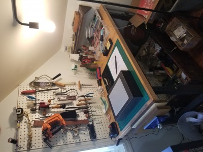
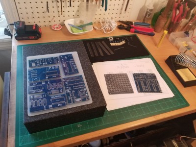
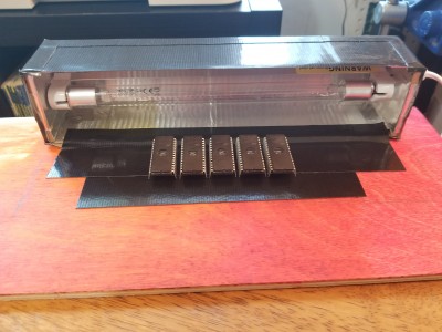
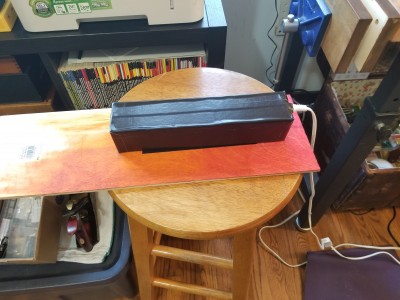
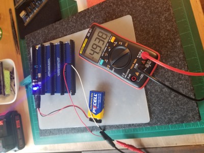
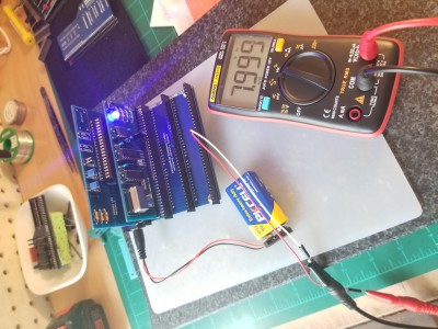
Anyway, here are some photos of the project, my little workspace, and a couple shots of my home-made EPROM de-programmer, just for fun:

Attachment:
20220324_110210.jpg
20220324_110210.jpg [ 3.28 MiB | Viewed 4548 times ]

Attachment:
20220324_114723.jpg
20220324_114723.jpg [ 3.94 MiB | Viewed 4548 times ]

Attachment:
20220325_100852.jpg
20220325_100852.jpg [ 3.75 MiB | Viewed 4548 times ]

Attachment:
20220327_180201.jpg
20220327_180201.jpg [ 3.35 MiB | Viewed 4548 times ]

Attachment:
20220327_180839.jpg
20220327_180839.jpg [ 3.63 MiB | Viewed 4548 times ]

Attachment:
20220331_132437.jpg
20220331_132437.jpg [ 3.65 MiB | Viewed 4548 times ]

Attachment:
20220331_132637.jpg
20220331_132637.jpg [ 3.33 MiB | Viewed 4548 times ]


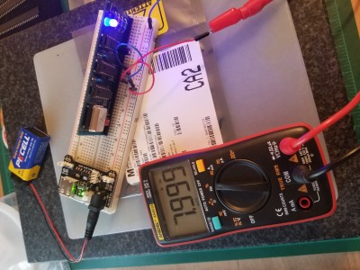
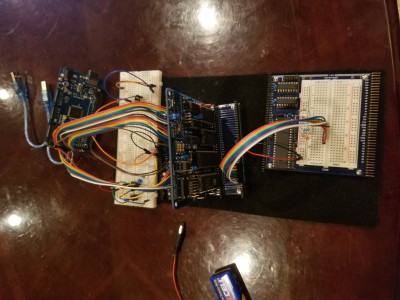
As far as I can tell with my little multimeter, everything is working out OK. The voltage regulator on the backplane seems to be working, the clock module is producing a steady 8Hmz. However, I have encountered a puzzlement. Here is my testing setup:

Attachment:
20220403_202811.jpg
20220403_202811.jpg [ 3.86 MiB | Viewed 4548 times ]


That's an Arduino running Ben Eater's 6502 bus monitor; on the left of the top (larger) breadboard is a single-step circuit; on the right is the reset button. The main event is the RC6502 SBC plugged into the RC6502 backplane. The SBC has RAM, ROM, and PIA disabled via jumpers; I didn't populate the clock (I'm using the single step circuit) and Arduino parts of the board. Even though there's an Arduino in this photo, I'm not really very interested in them, and I don't want to farm out all the most interesting parts of my computer (I.e., I/O) to a tiny but vastly more complex micro-controller. In the foreground is the RC6502 Project Board, which is not connected to anything; I'm just using its mini-breadboard to put out NOPS on the data bus.

Everything in that picture works as expected; the processor (a W65C02S6TPG-14 I ordered from Jameco) jumps to the end of its address space, jumps to $eaea, and starts reading and executing nops off of the data bus and counting through memory.

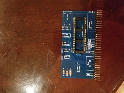
If I pull the SBC from the backplane and plug in this CPU module instead (using selfsame CPU):

Attachment:
20220403_202901.jpg
20220403_202901.jpg [ 4.26 MiB | Viewed 4548 times ]


The address lines fill with gibberish. The CPU board is such a simple one that I can't understand what I might have done to it that made it not work.

The schematic for the CPU module is here:

https://github.com/tebl/RC6502-Apple-1- ... %20CPU.pdf

And the schematic for the SBC is here:

https://github.com/tebl/RC6502-Apple-1- ... %20SBC.pdf

The only differences I spot concerning the CPU are that in the SBC pin 3 (PHIOut) is sent to the bus and pin 36 (BE) is pulled high through a resistor, whereas the CPU module leaves both of them unconnected. I can't see how PHIOut would have anything to do with what I'm seeing; the data-sheet from WDC is somewhat laconic about the BE pin.
Quote:
The Bus Enable input signal provides external control of the Address, Data and the RWB buffers. When Bus Enable is high, the Address, Data and RWB buffers are active. When BE is low, these buffers are set to the high impedance status. Bus Enable is an asynchronous signal.
Does "high impedance status" mean that the CPU is totally cut off from the address / data lines unless BE is pulled high?

I've done what testing I could think of with my multimeter, in terms of continuity testing all the pins on the connector against their corresponding pins on the CPU socket; the resistors are resisting. I'm stumped! I don't have an oscilloscope; short of getting one, is there any other troubleshooting I could try? Should I just try re-making the CPU module? My soldering has improved since then (it was one of the first ones I did), and I also refurbished my soldering iron with better temperature control (it was running WAAAAY too hot).

(Also, all of the photos I included seem to be sideways... I don't spot a way to rotate them inline, but if you click through to the larger version, my orientation descriptions make more sense! :lol: )

_________________
"The key is not to let the hardware sense any fear." - Radical Brad


Top
 Profile  
Reply with quote  
PostPosted: Mon Apr 04, 2022 6:48 am 
Offline
User avatar

Joined: Thu May 28, 2009 9:46 pm
Posts: 8177
Location: Midwestern USA
Paganini wrote:
The only differences I spot concerning the CPU are that in the SBC pin 3 (PHIOut) is sent to the bus...

WDC no longer recommends the use of Ø1 and Ø2 out. Those signals exist primarily to support older systems that relied on those outputs for clock signals. Neither is tested in production and WDC doesn’t even guarantee the two signals will be exactly 180 degrees out of phase, or by how much they will lag the clock input. Best if you follow their recommendations.

Quote:
...and pin 36 (BE) is pulled high through a resistor, whereas the CPU module leaves both of them unconnected.

As a general rule, no inputs on any CMOS device should be allowed to float. All inputs should be driven or pulled up/down. If a CMOS input is left floating it will likely pick up noise and cause the device to do silly things.

Quote:
the data-sheet from WDC is somewhat laconic about the BE pin...When Bus Enable is high, the Address, Data and RWB buffers are active. When BE is low, these buffers are set to the high impedance status...Does "high impedance status" mean that the CPU is totally cut off from the address / data lines unless BE is pulled high?

When BE is high, the 65C02 will drive all of its outputs. When BE is low, A0-15, D0-7 and RWB will go to the high-Z state, meaning those outputs will not drive anything and will look like an open circuit to anything connected to them. This feature makes it possible for something else to take over the buses, e.g., a DMA controller.

Quote:
I've done what testing I could think of with my multimeter, in terms of continuity testing all the pins on the connector against their corresponding pins on the CPU socket; the resistors are resisting. I'm stumped!

Try pulling BE up to VCC with a 3.3K resistor and see what happens.

Quote:
(Also, all of the photos I included seem to be sideways... I don't spot a way to rotate them inline, but if you click through to the larger version, my orientation descriptions make more sense! :lol: )

Just as toilets make lousy drinking fountains (unless you’re a dog :D), cell phones make lousy cameras. You probably need to invest in a cheap digital camera and some image editing software so your pictures turn out clear and correctly oriented.

Incidentally, the PDFs with your schematics can be attached to your posts, same as pictures. Some of us don’t do Github. :)

_________________
x86?  We ain't got no x86.  We don't NEED no stinking x86!


Top
 Profile  
Reply with quote  
PostPosted: Mon Apr 04, 2022 3:28 pm 
Offline

Joined: Fri Mar 18, 2022 6:33 pm
Posts: 443
BigDumbDinosaur wrote:

Quote:
...and pin 36 (BE) is pulled high through a resistor, whereas the CPU module leaves both of them unconnected.

As a general rule, no inputs on any CMOS device should be allowed to float. All inputs should be driven or pulled up/down. If a CMOS input is left floating it will likely pick up noise and cause the device to do silly things.

When BE is high, the 65C02 will drive all of its outputs. When BE is low, A0-15, D0-7 and RWB will go to the high-Z state, meaning those outputs will not drive anything and will look like an open circuit to anything connected to them. This feature makes it possible for something else to take over the buses, e.g., a DMA controller.


Well shi..gee that sucks. After I posted last night I continued searching and found this thread: viewtopic.php?f=4&t=6153 (Apparently, searching for "WD65C02 BE PIN" will provide bupkis, but "W65C02" all by itself will get you just what you're looking for... go figure.)

It appears that although the schematic lists U1 as W65C02, and the *actual silkscreen* on the PCB labels it as W65C02, and even though there's a jumper for VP ground (!), a W65C02 will not actually work on the CPU module, due to BE left unconnected. That's frustrating!

BigDumbDinosaur wrote:

Incidentally, the PDFs with your schematics can be attached to your posts, same as pictures. Some of us don’t do Github. :)


Ah, good tip; I'll keep that in mind.

Thanks!

_________________
"The key is not to let the hardware sense any fear." - Radical Brad


Top
 Profile  
Reply with quote  
PostPosted: Mon Apr 04, 2022 4:41 pm 
Offline

Joined: Fri Mar 18, 2022 6:33 pm
Posts: 443
BigDumbDinosaur wrote:
Try pulling BE up to VCC with a 3.3K resistor and see what happens.


That did the trick! Woop woop!

Thank you!

_________________
"The key is not to let the hardware sense any fear." - Radical Brad


Top
 Profile  
Reply with quote  
PostPosted: Mon Apr 04, 2022 8:04 pm 
Offline
User avatar

Joined: Thu May 28, 2009 9:46 pm
Posts: 8177
Location: Midwestern USA
Paganini wrote:
It appears that although the schematic lists U1 as W65C02, and the *actual silkscreen* on the PCB labels it as W65C02, and even though there's a jumper for VP ground (!), a W65C02 will not actually work on the CPU module, due to BE left unconnected. That's frustrating!

Pin 36 of the NMOS 6502 is a no-connect, whereas it’s BE on the WDC 65C02. The meaning of “no-connect” varies; in some cases, it’s just a pin with no connection, but in other cases, it is internally attached to something and hence should not be externally connected.

If I were making a “universal” MPU module, I’d have jumper blocks on it to isolate/connect pins 1, 5 and 36. Doing so would make it possible for the module to accept any type of 6502, meaning an NMOS part, any of the non-WDC CMOS parts, e.g., the Rockwell R65C02, or the WDC part. Pin 1 is ground on non-WDC parts, but is VPB on the WDC 65C02, which is an active output. Needless to say, you wouldn’t want that grounded.

Pin 5 is a no-connect on a 6502 or non-WDC 65C02, but is MLB on the WDC 65C02, which is also an active output. While pin 5 could be left unconnected in any case, MLB might be of interest with the WDC part. So I’d make a provision to be able to use it, same as with VPB.

The other pin to watch out for is SOB (pin 38). SOB is an edge-sensitive input that when asserted will set the overflow (v) bit in the status register. SOB should always be pulled up to Vcc to avoid v being randomly set and causing otherwise-inexplicable logic errors in programs that depend upon its status following an instruction that affects it, e.g., BIT. If no use of SOB is planned, it is safe to tie it directly to VCC and save the “cost” of a resistor.

Lastly, RDY on the WDC 65C02 is bi-directional and should never be tied directly to VCC. When the MPU executes a WAI instruction, it will drive RDY low. If RDY is tied direct to VCC, the MPU will try to sink the power supply when WAI is executed, resulting in a major malfunction. Typically, a 3.3K pullup is used in circuits that don’t use RDY. If RDY is to be driven by the output of another device, it must be connected to that device through a Schottky diode, or through a resistor of a sufficient value to limit current flow to a safe level. If the diode method is used, the need for a pullup remains, since the driving device can only pull RDY low.

Given the performance, flexibility and ready-availability of the WDC 65C02, I can’t fathom why anything that is newly-designed would be meant for use with an NMOS part. But, that's just me being a curmudgeon. :D

_________________
x86?  We ain't got no x86.  We don't NEED no stinking x86!


Top
 Profile  
Reply with quote  
PostPosted: Tue Apr 05, 2022 4:33 pm 
Offline

Joined: Fri Mar 18, 2022 6:33 pm
Posts: 443
BigDumbDinosaur wrote:

Given the performance, flexibility and ready-availability of the WDC 65C02, I can’t fathom why anything that is newly-designed would be meant for use with an NMOS part. But, that's just me being a curmudgeon. :D


The RC6502 was originally designed as an Apple 1 Replica, following Tom Owad's book "Apple 1 Replica Creation, Back to the garage." My guess is that it has slowly been modernized piecemeal as hobbyist interest has grown. (Some of the older boards still list 74LS series logic in their BOM, for example.) I think the other pins you mention are managed adequately, although pin 5 is NC rather than jumpered. I guess one might say it is "second-best practice." ;)

Attachment:
Screen Shot 2022-04-05 at 12.28.36 PM.png
Screen Shot 2022-04-05 at 12.28.36 PM.png [ 103.97 KiB | Viewed 4430 times ]

_________________
"The key is not to let the hardware sense any fear." - Radical Brad


Top
 Profile  
Reply with quote  
PostPosted: Tue Apr 05, 2022 8:19 pm 
Offline
User avatar

Joined: Thu May 28, 2009 9:46 pm
Posts: 8177
Location: Midwestern USA
Paganini wrote:
Attachment:
Screen Shot 2022-04-05 at 12.28.36 PM.png

:D I can't read that illustration because it’s in color—I’m partially color-blind.

_________________
x86?  We ain't got no x86.  We don't NEED no stinking x86!


Top
 Profile  
Reply with quote  
PostPosted: Thu Apr 07, 2022 10:52 am 
Offline
User avatar

Joined: Thu Dec 11, 2008 1:28 pm
Posts: 10800
Location: England
All working now? That's great! Thanks for sharing your design and your story.

(For the photos: it should be enough to do a trivial edit on your computer just before you attach: a series of 90 degree rotations is suitably lossless.)


Top
 Profile  
Reply with quote  
PostPosted: Thu Apr 07, 2022 2:33 pm 
Offline

Joined: Fri Mar 18, 2022 6:33 pm
Posts: 443
Hi Ed,

Yes, it's working! I made some progress this week; it has an RC Project Platform board hooked up to it now, with an LCD so it can actually do output. I'm planning to write a RAM test program for it over the weekend; I'll post some more photos when that's done. (I'll be sure to spin them around a few times first! :D )

_________________
"The key is not to let the hardware sense any fear." - Radical Brad


Top
 Profile  
Reply with quote  
PostPosted: Mon Apr 11, 2022 1:39 am 
Offline

Joined: Fri Mar 18, 2022 6:33 pm
Posts: 443
Blue April is up and running just fine (as far as I can tell, anyway) at 8Mhz.

Attachment:
20220410_211707.jpg
20220410_211707.jpg [ 2.92 MiB | Viewed 4270 times ]


Here's a side view so you can see her boards:

Attachment:
20220410_211750.jpg
20220410_211750.jpg [ 3.65 MiB | Viewed 4270 times ]


I did work on a RAM testing program - I found an algorithm in an old research report called "Random Access Memory Testing: Theory and practice The Gains of Fault Modelling by P.K. Veenstra" from Eindhoven University of Technology Netherlands that seems interesting and is conceptually simple - but it isn't finished yet because I got tangled up with addressing modes. All the indirect indexed modes I want to use only work in the Zero Page, which I didn't realize until just a while ago. Always read the fine print!

_________________
"The key is not to let the hardware sense any fear." - Radical Brad


Top
 Profile  
Reply with quote  
PostPosted: Mon Apr 11, 2022 11:07 am 
Offline

Joined: Tue Sep 03, 2002 12:58 pm
Posts: 298
Paganini wrote:
All the indirect indexed modes I want to use only work in the Zero Page, which I didn't realize until just a while ago.


You should still be able to use them. It's only the pointer that has to go in page zero. The location it points to can be anywhere.

Code:
    lda #$30
    sta zp
    lda #$12
    sta zp+1
    ldy #4
    lda (zp), Y


This sets up a pointer to location $1230 in the zero page locations 'zp' and 'zp+1'. The final LDA reads this pointer, adds Y to it (in this case Y is 4, giving $1234), then reads from that location. By changing the contents of zp and zp+1, you can access any location in memory.

It's common to either store 0 in the low byte of the pointer and use Y for the 'real' low byte, or to put the low byte of the target address in the pointer and make sure Y is zero.


Top
 Profile  
Reply with quote  
PostPosted: Mon Apr 11, 2022 1:35 pm 
Offline

Joined: Fri Mar 18, 2022 6:33 pm
Posts: 443
Yarr. I was trying to keep the pointers in ROM and skip a step (since it's a RAM test, you should really use ZP until after it's tested... :)

_________________
"The key is not to let the hardware sense any fear." - Radical Brad


Top
 Profile  
Reply with quote  
PostPosted: Mon Apr 11, 2022 3:37 pm 
Offline

Joined: Fri Mar 18, 2022 6:33 pm
Posts: 443
RAM test is now working! No new picture, because it looks just like the last one, except the LCD now says "RAM OK"

Turns out that my RAM test has actually been working for a while and doing what it was supposed to do: detecting hardware problems! Of course, my assumption (for a long time!) was that my hardware is a "known good configuration" and that my programming logic was at fault. But actually, the WDC processor I had in there won't pass the RAM test even at 250Khz. I swapped it out for a CMD one, and it works fine at 4Mhz. I'm guessing that this is a clock / timing related issue; I read in the Primer that the WDC chips are fussy about clock signals, and the RC6502 clock signal comes in over the bus.

_________________
"The key is not to let the hardware sense any fear." - Radical Brad


Top
 Profile  
Reply with quote  
PostPosted: Mon Apr 11, 2022 5:44 pm 
Offline
User avatar

Joined: Thu Dec 11, 2008 1:28 pm
Posts: 10800
Location: England
Oh, that's a result!


Top
 Profile  
Reply with quote  
PostPosted: Mon Apr 11, 2022 11:28 pm 
Offline
User avatar

Joined: Fri Dec 11, 2009 3:50 pm
Posts: 3354
Location: Ontario, Canada
Paganini wrote:
I read in the Primer that the WDC chips are fussy about clock signals, and the RC6502 clock signal comes in over the bus.
That's worth looking into. Meanwhile, here's an alternative theory. It may be that the problem has to do with what's going out of the WDC, not what's coming in. Compared with vintage NMOS and CMOS 65xx processors, modern WDC chips have substantially faster rise and fall times on their outputs. This can result in ringing and other AC performance issues, even at low clock speeds.

-- Jeff

_________________
In 1988 my 65C02 got six new registers and 44 new full-speed instructions!
https://laughtonelectronics.com/Arcana/ ... mmary.html


Top
 Profile  
Reply with quote  
Display posts from previous:  Sort by  
Post new topic Reply to topic  [ 256 posts ]  Go to page 1, 2, 3, 4, 5 ... 18  Next

All times are UTC


Who is online

Users browsing this forum: No registered users and 9 guests


You cannot post new topics in this forum
You cannot reply to topics in this forum
You cannot edit your posts in this forum
You cannot delete your posts in this forum
You cannot post attachments in this forum

Search for:
Jump to:  
cron