6502.org Forum  Projects  Code  Documents  Tools  Forum
It is currently Wed May 08, 2024 3:33 am

All times are UTC


Post new topic Reply to topic  [ 38 posts ]  Go to page 1, 2, 3  Next
Author Message
 Post subject: SRAM mystery
PostPosted: Wed Oct 06, 2021 8:57 pm 
Offline

Joined: Tue Jul 05, 2005 7:08 pm
Posts: 993
Location: near Heidelberg, Germany
Hi there,

I want to share an experience that leaves me somewhat puzzled.

Short summary: it took me about 2 weeks hardware debugging to find out that of the two chips of seemingly identical functionality, namely BSI BS62LV4006PIP55 and Alliance AS6C4008-55PCN, only the Alliance chip works in my computer, the other produces random errors. And I have no idea why...

Long story:

I want to resurrect my CaSpAer computer (aka CS/A65 http://www.6502.org/users/andre/csa/index.html ). To make sure to have a stable system, I have adapted the "8296 burnin" program from the Commodore PET to have a repeatedly running RAM test. See https://github.com/fachat/cbm-burnin-tests
What that test showed me was that after a few minutes random errors appeared in the RAM test for the VMEM (video memory, actually dRAM on the video card), but also in the static RAM ($0200-$8000). Before the tests I was assuming the stability problems I had were coming from using the video card with its dRAM (2x 41464), so I was primarily looking for problems there - however when I saw the SRAM errors (using the BSI chip), I assumed some common problem.

What irritated me was that the errors did not seem to have address patterns, were both of the Read or Write error (Read error is when the data is correctly read again after a first errornous read, Write error is when the data stays incorrect), and also bits did not seem to matter. And those errors happened both in the SRAM test and the VMEM (dRAM test).

So I was looking into the bus drivers on the CPU board (changing between ALS and HCT did not change it). I was looking into bus termination (5k6 to 5V, 3k3 to GND) did not change it. I was improving the backplane's capability to supply 5V - did not change. Switching between 1MHz (40col) and 2MHz (80col) did not change anything.

I then really started focusing on the SRAM, because that was the easier signal path.

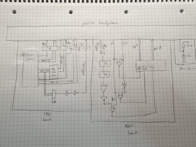
For the signal path see here:
https://flic.kr/p/2mxZNtj
Attachment:
File comment: Signal paths
20211006_180828_1920x1080.jpg
20211006_180828_1920x1080.jpg [ 1.41 MiB | Viewed 1677 times ]


Signals go from the CPU board to the BIOS board with the SRAM. Most signals are straightforward, only higher address lines go through some more complex selection logic. I only drew the a simple version with the ICs on it, to find out the longest (slowest) signal path.
You can find the schematics here: 
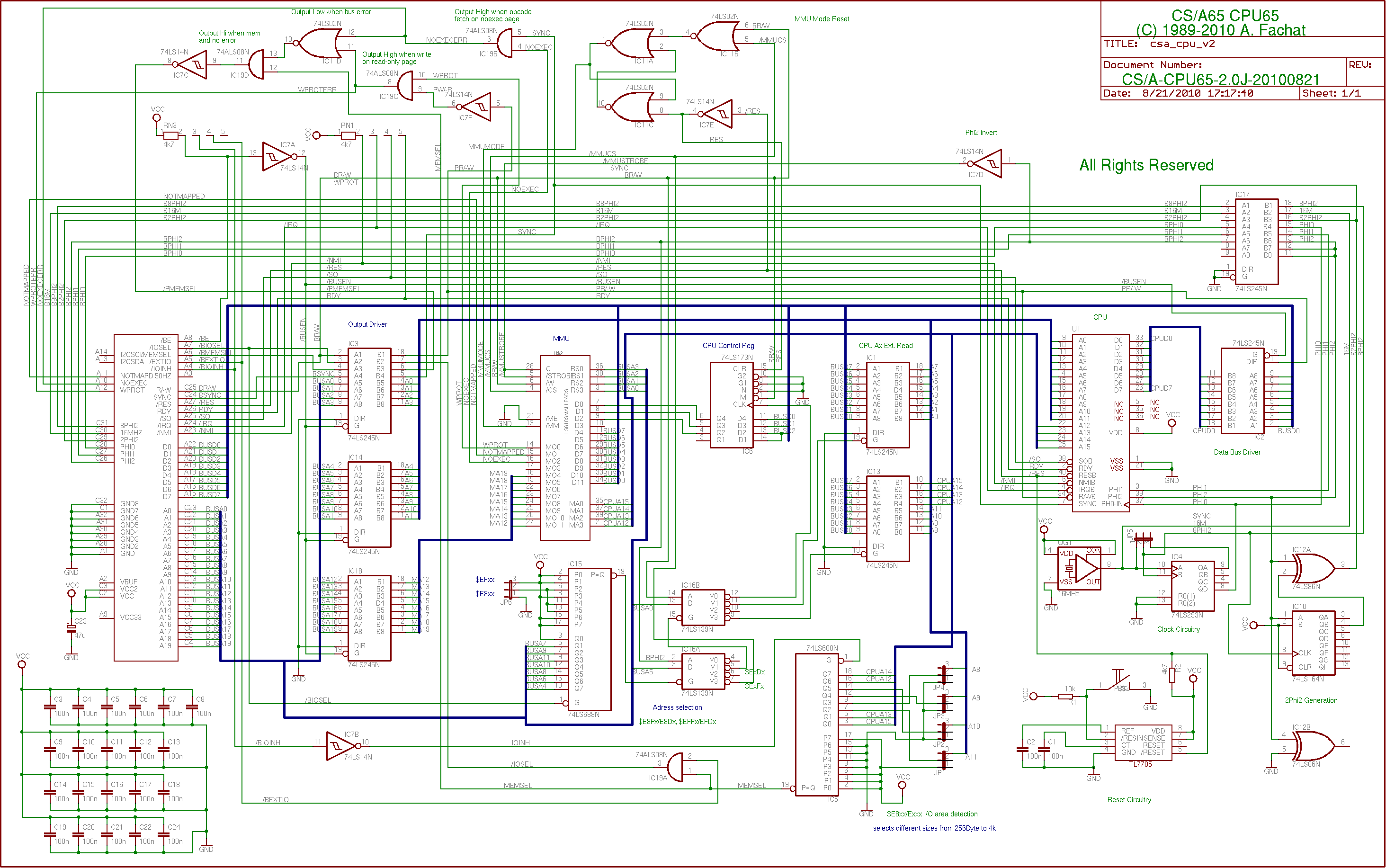
http://www.6502.org/users/andre/csa/cpu ... 0k_sch.png (CPU) and 
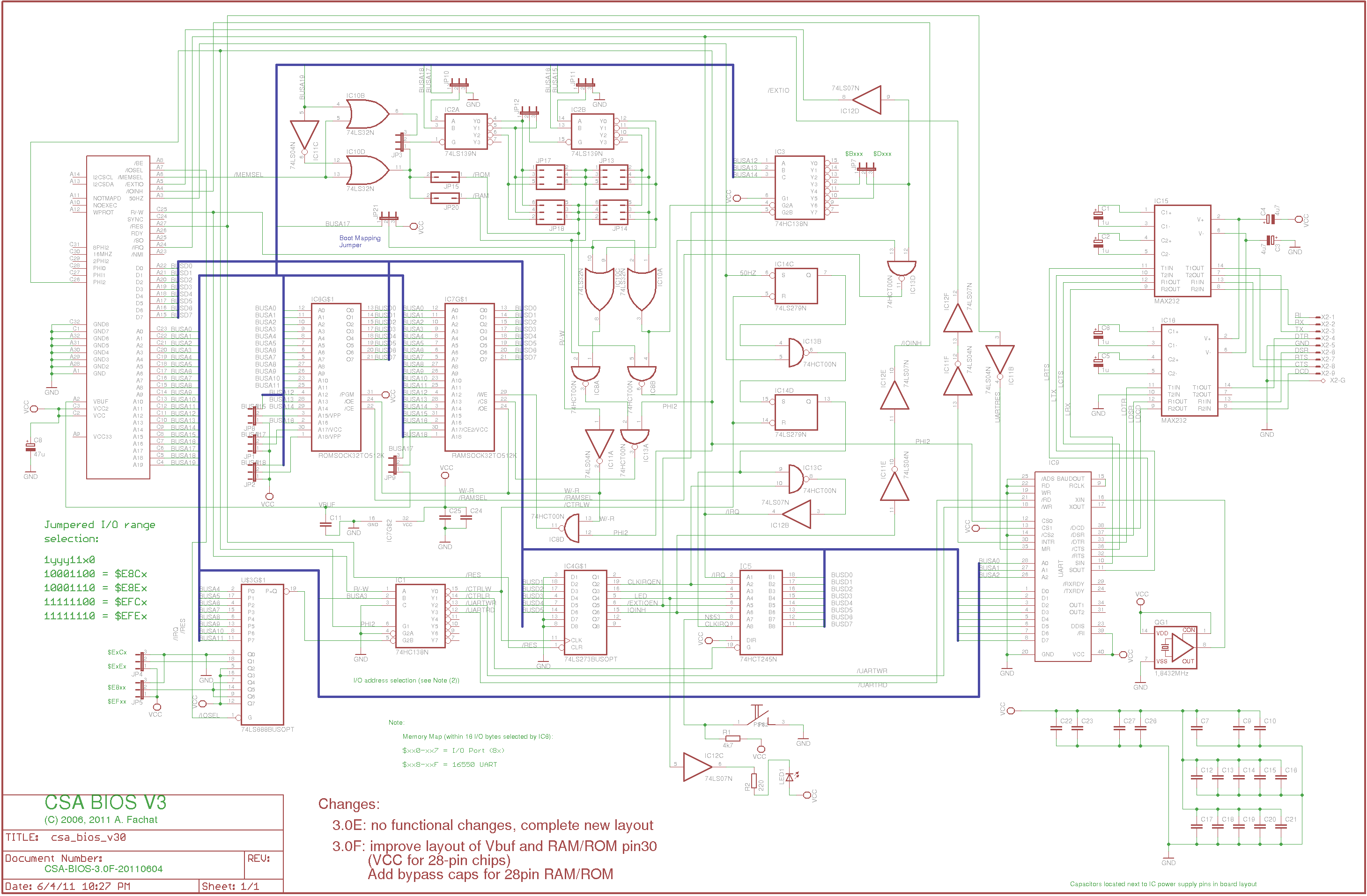
http://www.6502.org/users/andre/csa/bio ... 0f-sch.png (BIOS)

The longest path is in the /CS line - however, when scoping the signal I found that, before qualifying it with Phi2, it was only about 80ns after Phi2 falling (from the previous cycle, so about at least 150ns _before_ it would be active on /CS due to NANDing it with Phi2, so no timing problem here.
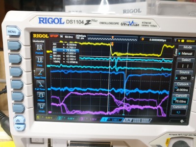
https://flic.kr/p/2mxZNwW
Attachment:
File comment: Address select
20211006_220712_1920x1080.jpg
20211006_220712_1920x1080.jpg [ 1.71 MiB | Viewed 1677 times ]

The yellow signal is Phi2, light blue is address line A0, violet is D0 (all from the bus), and dark blue is the RAM select line taken from the BIOS card directly before NANDing it with Phi2.

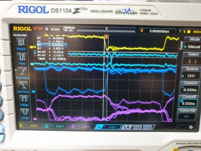
The next signals I looked at were /WE and /CS regarding Phi2 and Data bus.
https://flic.kr/p/2mxZNvo
Attachment:
File comment: /CE and /WE timing
20211006_220255_1920x1080.jpg
20211006_220255_1920x1080.jpg [ 1.8 MiB | Viewed 1677 times ]

The dark blue here is /WE, the others as described above. So /WE goes high about 16ns after Phi2 goes low, while the databus is still valid. /CS and /OE look the same.

Finally, as I was pretty desperate, I switched to another SRAM chip from a different supplier (Alliance). And, suddenly, all errors completely went away! Even the VMEM (dRAM) tests suddenly worked flawlessly. The latter I assume seem to have come because the test itself was running in the (assumed more stable) SRAM...
https://flic.kr/p/2my8oYp
Attachment:
File comment: Successful RAM test
20211005_225955_1920x1080.jpg
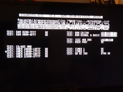
20211005_225955_1920x1080.jpg [ 1.55 MiB | Viewed 1677 times ]

(Ignore the header line except the number of cycles that tell how often the test has ran, also the other errors are known and of no significance - important are the OK on the RAM tests)

I then checked two other chips of the same type from BSI, all had the same problem! I only have that one Alliance chip, but that works flawlessly.

So, I looked at the datasheets of these two chips, but could not find any significant difference (if I haven't overlooked anything).
Driver capacity was the same (up to 1mA IIRC) to drive against termination resistors, but with or without termination resistors on the bus did not change it. Comparing the timing against the scope measurements seems to be totally valid.
10mA is the same power requirements for both chips at 1MHz, which is reasonable. The chips even has extra supply lines directly from the bus connector and an extra 100nF cap soldered to it.

So I am really out of ideas what could be the reason for this problem.

Do you have any ideas what I could check?

_________________
Author of the GeckOS multitasking operating system, the usb65 stack, designer of the Micro-PET and many more 6502 content: http://6502.org/users/andre/


Top
 Profile  
Reply with quote  
 Post subject: Re: SRAM mystery
PostPosted: Thu Oct 07, 2021 12:41 am 
Offline
User avatar

Joined: Sun Jun 30, 2013 10:26 pm
Posts: 1928
Location: Sacramento, CA, USA
I am by no stretch of the imagination a 'scope expert, but it looks to my untrained eye like your data bus is a bit flaky. I understand that some floating is to be expected during phi2 low, but it doesn't look very confidence-inspiring while phi2 is high either.

_________________
Got a kilobyte lying fallow in your 65xx's memory map? Sprinkle some VTL02C on it and see how it grows on you!

Mike B. (about me) (learning how to github)


Top
 Profile  
Reply with quote  
 Post subject: Re: SRAM mystery
PostPosted: Thu Oct 07, 2021 1:01 am 
Offline
User avatar

Joined: Thu May 28, 2009 9:46 pm
Posts: 8176
Location: Midwestern USA
Could you please post the data sheets for the two SRAMs involved?

Also, in the scope samples, is the MPU reading or writing? Is the MPU NMOS or CMOS?

_________________
x86?  We ain't got no x86.  We don't NEED no stinking x86!


Top
 Profile  
Reply with quote  
 Post subject: Re: SRAM mystery
PostPosted: Thu Oct 07, 2021 1:21 am 
Offline
User avatar

Joined: Fri Dec 11, 2009 3:50 pm
Posts: 3354
Location: Ontario, Canada
fachat wrote:
So, I looked at the datasheets of these two chips, but could not find any significant difference (if I haven't overlooked anything).

Interesting problem!

Since you're asking for assistance, maybe you could make it easy for us and anticipate the info we'll need. Can you post the two datasheets, please? (This'll save us from having to go find them). :wink:

-- Jeff

edit: whoops, I see BDD is thinking along the same lines! :)

_________________
In 1988 my 65C02 got six new registers and 44 new full-speed instructions!
https://laughtonelectronics.com/Arcana/ ... mmary.html


Last edited by Dr Jefyll on Thu Oct 07, 2021 2:00 am, edited 1 time in total.

Top
 Profile  
Reply with quote  
 Post subject: Re: SRAM mystery
PostPosted: Thu Oct 07, 2021 1:43 am 
Offline

Joined: Fri Dec 21, 2018 1:05 am
Posts: 1076
Location: Albuquerque NM USA
I'm intrigued by the statement that "after a few minutes random errors appeared ...". Why after a few minutes? Did a device got hot? Was there an intermittent connection changed due to warming up? Does the problem changes if you flex the boards or apply pressure to various parts? This may be a system noise problem so does raising voltage to 5.4V (increase system noise) or lowering voltage to 4.6V (decrease system noise) change anything?
Bill


Top
 Profile  
Reply with quote  
 Post subject: Re: SRAM mystery
PostPosted: Thu Oct 07, 2021 2:31 am 
Offline
User avatar

Joined: Tue Mar 05, 2013 4:31 am
Posts: 1373
An interesting problem of course... here's the datasheets:

Attachment:
AS6C4008.pdf [716.68 KiB]
Downloaded 40 times


Attachment:
datasheet(6).pdf [375.4 KiB]
Downloaded 33 times


As noted, the published specifications don't show any real difference, hence the confusion.

I recently had a similar issue using an older 70ns Alliance 32KB SRAM replacing it with the newer version which is a 55ns Alliance 32KB SRAM. In my situation, the newer 55ns part would not work. I ended up replacing the ATF22V10CQZ glue chip with an ATF22V10C glue chip and that resolved the problem. Granted, I can't pinpoint any significant difference between the two Atmel parts to account for the issue.

If it's heat related (as Bill suggested) than a quick shot of Freon should be able to sort that one out. I'm thinking more along the lines of voltage levels being on the edge, or slew rate creating a slim timing issue to have the required minimum voltage when needed... and perhaps the one SRAM is on the edge of it's spec if this happens. If noise is a suspected problem, then perhaps better decoupling/bypass may change the results.

Beyond this... I think we're mostly guessing at things to check and/or look for.

_________________
Regards, KM
https://github.com/floobydust


Top
 Profile  
Reply with quote  
 Post subject: Re: SRAM mystery
PostPosted: Thu Oct 07, 2021 4:30 am 
Offline
User avatar

Joined: Thu May 28, 2009 9:46 pm
Posts: 8176
Location: Midwestern USA
floobydust wrote:
I'm thinking more along the lines of voltage levels being on the edge, or slew rate creating a slim timing issue to have the required minimum voltage when needed... and perhaps the one SRAM is on the edge of it's spec if this happens. If noise is a suspected problem, then perhaps better decoupling/bypass may change the results.

That is what I was getting at when I asked if the MPU is NMOS or CMOS and if we are seeing a read or write cycle (I'm having a little trouble analyzing the scope display due to some of the colors). The NMOS part's outputs are on the weak side and if one can believe the scope traces, it appears the data bus signal is a little too low to produce a solid logic 1 at TTL levels.

_________________
x86?  We ain't got no x86.  We don't NEED no stinking x86!


Top
 Profile  
Reply with quote  
 Post subject: Re: SRAM mystery
PostPosted: Thu Oct 07, 2021 6:18 am 
Offline

Joined: Tue Jul 05, 2005 7:08 pm
Posts: 993
Location: near Heidelberg, Germany
Thanks for your replies! And thanks to Floobydust for posting the datasheets.
Sorry it was late last night when I wrote this and I have been missing some details because I am so used to them...

A couple of thoughts:
- The signals are all taken from the backplane (except the SRAM selects). So there is a 74ALS245 between this signal and the CPU.
- The CPU is a R65C02P4, a 4MHz Rockwell CMOS version.
- when I tested it yesterday, the errors came dripping in, one each few minutes or so. So I can't really test if using cold spray reduces error rate or I would spend a whole bottle without result. I could only test if making it cold breaks it. I _did_ test with a cold system though this morning. It seems the errors actually appearing faster.
- flexing the board: I ruled that out as I am regularly taking the BIOS board out from the system and putting back in, and it still was consistently the BSI chips failing, the Alliance chip working
- Power supply - It is currently connected to a PC power supply using a floppy-type power connector, I do have a lab power supply so using variating voltages is still on my list. But then why still BSI consistently (across multiple parts) faulty while Alliance works, when the datasheets looks similar?
- Regarding the scope shots: in fact the databus lines are misleading. I took new scope shots this morning that actually revealed something... see next post

_________________
Author of the GeckOS multitasking operating system, the usb65 stack, designer of the Micro-PET and many more 6502 content: http://6502.org/users/andre/


Top
 Profile  
Reply with quote  
 Post subject: Re: SRAM mystery
PostPosted: Thu Oct 07, 2021 6:23 am 
Offline

Joined: Tue Jul 05, 2005 7:08 pm
Posts: 993
Location: near Heidelberg, Germany
I have let the CPU run a simple loop (JMP to *) in the SRAM and took scope shots again.

Again, yellow is Phi2 on the backplane, blue is A0 on the backplane, and violet is D0 on the backplane.

This is the working chip:
Attachment:
File comment: Working Alliance chip
20211007_080750_1920x1080.jpg
20211007_080750_1920x1080.jpg [ 1.77 MiB | Viewed 1627 times ]


This is the one that breaks:
Attachment:
File comment: BSI with faults...
20211007_080504_1920x1080.jpg
20211007_080504_1920x1080.jpg [ 1.77 MiB | Viewed 1627 times ]


Now that's surprising, given that /CE, /OE and /WE are all qualified with Phi2....
(I'll verify this this evening, and maybe take some shots where /CE is not qualified)

André

_________________
Author of the GeckOS multitasking operating system, the usb65 stack, designer of the Micro-PET and many more 6502 content: http://6502.org/users/andre/


Top
 Profile  
Reply with quote  
 Post subject: Re: SRAM mystery
PostPosted: Thu Oct 07, 2021 8:35 am 
Offline
User avatar

Joined: Fri Nov 09, 2012 5:54 pm
Posts: 1393
Nothing obvious in the oscilloscope pictures and in the SRAM datasheets.

Since the ViH and ViL definitions don't look too different for both chips,
I can't tell if this is relevant here, but:
;
Voltage reference level for the timing diagrams in the datasheets is
1.5V for AS6C4008 (Alliance, working) and 2.5V for BS65LV4006 (BSI, not working).

;---

AS6C4008 //Alliance, working
Vil<=0.8V, ViH>=2.4V //at VCC=4.5V..5.5V
Input rise and fall times 3ns
Input and output timing reference levels 1.5V //Datasheet page 4: AC test conditions

BS65LV4006 //BSI, not working
ViL<=0.8V, ViH>=2.2V //at VCC=5.0V
Input rise and fall times 1V/ns
Input and output timing reference levels 0.5*VCC =2.5V //Datasheet page 4: AC test conditions

Hmm... are you using 74LS245 as backplane drivers ?
74LS245 VoH is 2.4V min. at IoH=-3mA and VCC=4.75V


Top
 Profile  
Reply with quote  
 Post subject: Re: SRAM mystery
PostPosted: Thu Oct 07, 2021 9:03 am 
Offline

Joined: Tue Jul 05, 2005 7:08 pm
Posts: 993
Location: near Heidelberg, Germany
Bus drivers are HCT. There was noch change in the situation when switching between ALS and HCT.

_________________
Author of the GeckOS multitasking operating system, the usb65 stack, designer of the Micro-PET and many more 6502 content: http://6502.org/users/andre/


Top
 Profile  
Reply with quote  
 Post subject: Re: SRAM mystery
PostPosted: Thu Oct 07, 2021 9:03 am 
Offline

Joined: Tue Jul 05, 2005 7:08 pm
Posts: 993
Location: near Heidelberg, Germany
Both datasheets state that they are TTL compatible... for whatever that means.

_________________
Author of the GeckOS multitasking operating system, the usb65 stack, designer of the Micro-PET and many more 6502 content: http://6502.org/users/andre/


Top
 Profile  
Reply with quote  
 Post subject: Re: SRAM mystery
PostPosted: Thu Oct 07, 2021 9:06 am 
Offline

Joined: Tue Jul 05, 2005 7:08 pm
Posts: 993
Location: near Heidelberg, Germany
What makes me wonder why the BSI chip first seems to put different values on the bus before quickly switching to the (assumed) correct value.

If during a write a different memory cell is addressed as well this might give a problem, what do you think?

_________________
Author of the GeckOS multitasking operating system, the usb65 stack, designer of the Micro-PET and many more 6502 content: http://6502.org/users/andre/


Top
 Profile  
Reply with quote  
 Post subject: Re: SRAM mystery
PostPosted: Thu Oct 07, 2021 9:25 am 
Offline

Joined: Sun Jun 29, 2014 5:42 am
Posts: 337
I would be tempted to try the following experiment: remove the Φ2 term from the RAM nCS signal.

You can do this by disconnecting the "nCS" NAND gate connection from Φ2 (by bending the IC leg out from the socket), and pulling it high with a 1K resistor.

This will allow a bit more time for the address to settle internally in the SRAM before the output is enabled, which might avoid the additional transitions on the data bus.

If that helps, we can start to theorise why....


Top
 Profile  
Reply with quote  
 Post subject: Re: SRAM mystery
PostPosted: Thu Oct 07, 2021 9:36 am 
Offline
User avatar

Joined: Fri Nov 09, 2012 5:54 pm
Posts: 1393
Attachment:
glitch.png
glitch.png [ 313.01 KiB | Viewed 1603 times ]

I think it would be worth to check if there is a spike\glitch on one of the address lines
(if there is one, maybe it's more confusing to BSI SRAMs than to Alliance SRAMs).

On second thought: "after a few minutes random errors appeared ..."
Have you tried how the BSI SRAM responds to cooling spray ?


Top
 Profile  
Reply with quote  
Display posts from previous:  Sort by  
Post new topic Reply to topic  [ 38 posts ]  Go to page 1, 2, 3  Next

All times are UTC


Who is online

Users browsing this forum: No registered users and 11 guests


You cannot post new topics in this forum
You cannot reply to topics in this forum
You cannot edit your posts in this forum
You cannot delete your posts in this forum
You cannot post attachments in this forum

Search for:
Jump to: