6502.org Forum  Projects  Code  Documents  Tools  Forum
It is currently Sun May 05, 2024 2:08 am

All times are UTC


Post new topic Reply to topic  [ 126 posts ]  Go to page 1, 2, 3, 4, 5 ... 9  Next
Author Message
PostPosted: Mon Sep 27, 2021 1:10 pm 
Offline
User avatar

Joined: Sat Jul 24, 2021 1:37 pm
Posts: 282
Hey everyone,

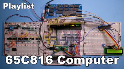
After cbmeeks posted the link to my new 65C816 computer YouTube series and seeing the interest that forum members had, I thought it would be a good idea to create a project thread to exchange ideas.

Here is the link to the playlist where you can watch it from the beginning:

Image

The goal of the project is to build a 65C816 development platform and learn about the CPU. I'm not going for ludicrous speed and features for revision A, here are the goals:

- Runs at 4Mhz
- Prototyped on a breadboard, through-hole ICs only, no programmable logic
- 32KB RAM, 32KB ROM, 512KB extended RAM
- 65C22 and 65C21 for peripheral I/O
- 65C51 for UART

Conceptually, it will be similar to WDC's own development board. I know the 65C51 has a bug but it seems like a good period-accurate starter, and I'll explore newer PLCC options in revision B.
The goal of the series is to provide a good description of all the design decisions, including going in-depth on timing, and be a more advanced complement to something like Ben Eater's 6502 series, as well as show more love to this cool CPU, that it currently lacks.

You can find the source (hardware, software, and documentation) for this project on my GitHub here: https://github.com/adrienkohlbecker/65C816

Once this first revision is complete, I'm thinking of using it to explore designs going in a few directions:

- Moving to surface mount, maybe even to 3.3V
- Programmable logic
- Video and keyboard I/O (could be TMS9918+PS/2?)
- Running at 14Mhz
- And a bunch more ideas floating in my head... probably won't have the time to do them all :)

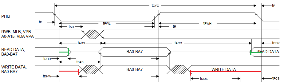
At this point in time, I'm exploring the Data Bus / Bank Address demultiplexing circuit, and improving the one shown in the datasheet by making it work in more situations (using BE, RDY). The next steps are to build a clock and reset circuit, and add memory.
I hope you enjoy this project and that this thread will spark some interesting conversations!

_________________
BB816 Computer YouTube series


Last edited by akohlbecker on Tue May 23, 2023 1:36 pm, edited 5 times in total.

Top
 Profile  
Reply with quote  
PostPosted: Mon Sep 27, 2021 1:11 pm 
Offline
User avatar

Joined: Sat Jul 24, 2021 1:37 pm
Posts: 282
The latest episode is #5, and discusses how to transform the RDY pin into two uni-directional signals, RDY_IN and WAITN. Hope you find it interesting!

This is the current schematic:

Attachment:
65C816.png
65C816.png [ 699.23 KiB | Viewed 7888 times ]

_________________
BB816 Computer YouTube series


Last edited by akohlbecker on Fri Oct 22, 2021 3:24 pm, edited 4 times in total.

Top
 Profile  
Reply with quote  
PostPosted: Mon Sep 27, 2021 1:18 pm 
Offline
User avatar

Joined: Thu Dec 11, 2008 1:28 pm
Posts: 10797
Location: England
Thanks for the new thread - and for delineating your goals up front. Always good to have clarity about what a project is aiming for, and what it isn't.


Top
 Profile  
Reply with quote  
PostPosted: Mon Sep 27, 2021 2:12 pm 
Offline
User avatar

Joined: Fri Dec 11, 2009 3:50 pm
Posts: 3351
Location: Ontario, Canada
akohlbecker wrote:
Hope you find it interesting!
I think we will!

akohlbecker, can I remind you that this forum allows you attach images and other attachments with your posts? I think you'll find this more convenient than off-site storage; also, it's more permanent (because of Mike's backup policy).

cheers,
Jeff

_________________
In 1988 my 65C02 got six new registers and 44 new full-speed instructions!
https://laughtonelectronics.com/Arcana/ ... mmary.html


Top
 Profile  
Reply with quote  
PostPosted: Fri Oct 22, 2021 3:30 pm 
Offline
User avatar

Joined: Sat Jul 24, 2021 1:37 pm
Posts: 282
Dr Jefyll wrote:
akohlbecker, can I remind you that this forum allows you attach images and other attachments with your posts? I think you'll find this more convenient than off-site storage; also, it's more permanent (because of Mike's backup policy).


Updated!

_________________
BB816 Computer YouTube series


Top
 Profile  
Reply with quote  
PostPosted: Fri Oct 22, 2021 3:39 pm 
Offline
User avatar

Joined: Sat Jul 24, 2021 1:37 pm
Posts: 282
The latest episode is #6 (released a couple weeks ago but forgot to post here!).

In that episode, I add support for RDY in my databus demultiplexing circuit. After decoding it into RDY_IN and WAITN in the previous episode, I can now use this signal to determine if I should open the latch and enable the buffer or not. Had to add a flip flop to register the RDY input so that the glue logic and the CPU are kept in sync, as well as a clock flip flop to make the timings work. I'm pretty happy with the results, but I'm now working on the next episode which will go back on the timings, and (spoiler alert), use a DS1035 delay line to make them work even better.

This is the new logic:

Attachment:
new logic.png
new logic.png [ 140.98 KiB | Viewed 7888 times ]


And of course this is the whole new schematic:

Attachment:
65C816.png
65C816.png [ 767.8 KiB | Viewed 7888 times ]


Hope you find this interesting!

_________________
BB816 Computer YouTube series


Top
 Profile  
Reply with quote  
PostPosted: Sun Oct 24, 2021 8:16 am 
Offline
User avatar

Joined: Mon Aug 30, 2021 11:52 am
Posts: 258
Location: South Africa
Hey, I'm really enjoying your series and I really like that you've gone into so much depth on the RDY pin; basically the one pin I had decided was too complicated and so I just ignored.

I'm also just done watching episode 7 which reminded me I have a question about read/write timing.

Image

If you take a look at tDSR does that mean that READ DATA must be valid (at 5V) 10ns before the clock falls? If so I assume that means that the 65C816 is constantly latching that READ data internally and needs it to be latched before the clock fall?

Also as tDHR is 10ns does that mean READ DATA actually needs to be valid for at leas 20ns in total (the green line)?

Thanks,
Andrew


Top
 Profile  
Reply with quote  
PostPosted: Sun Oct 24, 2021 8:35 am 
Offline
User avatar

Joined: Thu Dec 11, 2008 1:28 pm
Posts: 10797
Location: England
Even with a flop which captures data on the clock edge, there is usually a small setup time and a small hold time constraint both of which need to be satisfied for reliable operation. Which is to say, nothing is instantaneous, and there needs to be a little stability around the crucial moment.

In some cases the hold time will be zero, but it's still a constraint.

Internally, what may happen is that an unstable input at the critical moment will cause internal delay as the signal settles, which turns into a problem of getting the right answer in time for the next clock edge. Worse, it's possible that the slowly changing signal on the inside is interpreted as low by one part of the chip and high by another, which can cause completely unexpected results, or a lock up.

Search for 'metastability' for more on this.


Top
 Profile  
Reply with quote  
PostPosted: Sun Oct 24, 2021 11:24 am 
Offline
User avatar

Joined: Sat Jul 24, 2021 1:37 pm
Posts: 282
AndrewP wrote:
Hey, I'm really enjoying your series and I really like that you've gone into so much depth on the RDY pin; basically the one pin I had decided was too complicated and so I just ignored.


Thank you! :wink:

AndrewP wrote:
I'm also just done watching episode 7 which reminded me I have a question about read/write timing.

Image

If you take a look at tDSR does that mean that READ DATA must be valid (at 5V) 10ns before the clock falls? If so I assume that means that the 65C816 is constantly latching that READ data internally and needs it to be latched before the clock fall?

Also as tDHR is 10ns does that mean READ DATA actually needs to be valid for at leas 20ns in total (the green line)?

Thanks,
Andrew


Yes, that is my understanding as well. You need to present the data at the CPU pins 10ns before and 10ns after the falling edge of the clock. Note that the buffer that you add in front of the CPU impacts those timings: in my build using the 74ACT245, I need to present the data to the buffer 19ns before and 9ns after the falling edge of the clock. See this section of my timing diagram

Attachment:
Screenshot 2021-10-24 at 13.22.58.png
Screenshot 2021-10-24 at 13.22.58.png [ 94.76 KiB | Viewed 7814 times ]

_________________
BB816 Computer YouTube series


Top
 Profile  
Reply with quote  
PostPosted: Sun Oct 24, 2021 11:28 am 
Offline
User avatar

Joined: Sat Jul 24, 2021 1:37 pm
Posts: 282
As Andrew mentioned, the latest episode #7 got released yesterday!

In that episode, I go back on the timings of the databus demultiplexing circuit, and I add a delay of 10ns to some signals using a Maxim DS1035M-10, which is a pretty cool, accurate delay chip. This is the final episode in this demultiplexing series, and I'm now pretty happy with the circuit as is. In the next episode, I'll go back to basics and work on the clock!

Here is the new glue logic:

Attachment:
Screenshot 2021-10-24 at 13.27.39.png
Screenshot 2021-10-24 at 13.27.39.png [ 71.75 KiB | Viewed 7814 times ]


And the whole schematic

Attachment:
Screenshot 2021-10-24 at 13.27.58.png
Screenshot 2021-10-24 at 13.27.58.png [ 1.08 MiB | Viewed 7814 times ]

_________________
BB816 Computer YouTube series


Top
 Profile  
Reply with quote  
PostPosted: Sun Oct 24, 2021 8:00 pm 
Offline
User avatar

Joined: Thu May 28, 2009 9:46 pm
Posts: 8173
Location: Midwestern USA
AndrewP wrote:
Hey, I'm really enjoying your series and I really like that you've gone into so much depth on the RDY pin; basically the one pin I had decided was too complicated and so I just ignored.

You should know that the use of the 65C816's RDY input to wait-state a 65C816 with extended RAM presents some not-insignificant problems. While said problems aren't intractable and can be solved if you throw enough silicon at them (and are willing to put up with the resulting propagation delay), they are sufficiently onerous that alternate wait-state methods using clock stretching have been developed and tested. See here for some theory and practical application. Also, see here for a one-chip solution for the 65C02 or a 65C816 without extended RAM.

_________________
x86?  We ain't got no x86.  We don't NEED no stinking x86!


Top
 Profile  
Reply with quote  
PostPosted: Mon Oct 25, 2021 8:58 am 
Offline
User avatar

Joined: Mon Aug 30, 2021 11:52 am
Posts: 258
Location: South Africa
akohlbecker wrote:
... buffer 19ns before and 9ns after the falling edge of the clock. See this section of my timing diagram
BigEd wrote:
Internally, what may happen is that an unstable input at the critical moment...
Thanks! I had a suspicion that might be the case. Now I'm going to have even less time for address decode and reading *sigh*. Also thanks for pointing me to WaveDrom, that's going to come in handy in the future.

BigDumbDinosaur wrote:
...the 65C816's RDY input to wait-state a 65C816 with extended RAM presents some not-insignificant problems.
Yup, I've mostly got around this by using SRAM that's way faster than the 65816's clock rather than using the RDY pin. For slow devices I'm planning to use a FIFO and then poll it. *Not yet a well thought thought out plan but if I get it right I can use one FIFO for all my input devices.


Top
 Profile  
Reply with quote  
PostPosted: Mon Oct 25, 2021 9:16 am 
Offline
User avatar

Joined: Thu May 28, 2009 9:46 pm
Posts: 8173
Location: Midwestern USA
AndrewP wrote:
BigDumbDinosaur wrote:
...the 65C816's RDY input to wait-state a 65C816 with extended RAM presents some not-insignificant problems.

Yup, I've mostly got around this by using SRAM that's way faster than the 65816's clock rather than using the RDY pin.

I think you misunderstood what I said. It has nothing to do with the speed of SRAM. You should probably read the linked topics in my previous post before you go off on a tangent with a FIFO and use a battleship to sink a rowboat. :D

_________________
x86?  We ain't got no x86.  We don't NEED no stinking x86!


Top
 Profile  
Reply with quote  
PostPosted: Mon Oct 25, 2021 4:15 pm 
Offline
User avatar

Joined: Sat Jul 24, 2021 1:37 pm
Posts: 282
BigDumbDinosaur wrote:
AndrewP wrote:
Hey, I'm really enjoying your series and I really like that you've gone into so much depth on the RDY pin; basically the one pin I had decided was too complicated and so I just ignored.

You should know that the use of the 65C816's RDY input to wait-state a 65C816 with extended RAM presents some not-insignificant problems. While said problems aren't intractable and can be solved if you throw enough silicon at them (and are willing to put up with the resulting propagation delay), they are sufficiently onerous that alternate wait-state methods using clock stretching have been developed and tested. See here for some theory and practical application. Also, see here for a one-chip solution for the 65C02 or a 65C816 without extended RAM.


I'm curious to hear what the problems are with using RDY for wait states?

_________________
BB816 Computer YouTube series


Top
 Profile  
Reply with quote  
PostPosted: Mon Oct 25, 2021 4:59 pm 
Offline
User avatar

Joined: Thu Dec 11, 2008 1:28 pm
Posts: 10797
Location: England
I believe it's all about latching the upper address bits correctly: hence the pointer to a simple recipe if you don't need to do that.


Top
 Profile  
Reply with quote  
Display posts from previous:  Sort by  
Post new topic Reply to topic  [ 126 posts ]  Go to page 1, 2, 3, 4, 5 ... 9  Next

All times are UTC


Who is online

Users browsing this forum: No registered users and 13 guests


You cannot post new topics in this forum
You cannot reply to topics in this forum
You cannot edit your posts in this forum
You cannot delete your posts in this forum
You cannot post attachments in this forum

Search for:
Jump to: