6502.org Forum  Projects  Code  Documents  Tools  Forum
It is currently Sat May 04, 2024 10:31 am

All times are UTC


Post new topic Reply to topic  [ 54 posts ]  Go to page Previous  1, 2, 3, 4  Next
Author Message
PostPosted: Tue May 11, 2021 12:44 pm 
Offline
User avatar

Joined: Fri Dec 12, 2008 10:40 pm
Posts: 1000
Location: Canada
enso wrote:
BillO wrote:
...I honestly don't think it's much of an issue....


Yeah, except that if ignored, your design may not work. It probably will, but not necessarily.

Keep in mind that not only are WDC chips not TTL compatible, they are not even CMOS compatible - at least not with any 5V SRAM or EEPROM or FLASH that I've looked at. All the devices I've looked at specify minimum High voltage as 2.4V! Some parts even lower.
...


I think you either did not read everything I wrote or missed the point enso.

Did you look at that spec sheet? My point is, those older CMOS devices were on the market at a time when compliance with TTL specifications was paramount, so that is what the spec sheet shows. If those devices were still in production you would see specifications like in the spec sheet I posted, or they might not even bother with old TTL specs at all. Older devices, like say a 27C256 WILL reliably deliver CMOS performance into CMOS loads. Your design will not fail because of voltage issues.

Question for all. Has anyone here ever had a case where a 27C256 (or CMOS SRAM or CMOS PLD) would not work with a WDC (or other CMOS) CPU provided timing constraints were not overly abused?

I don't expect everyone here will have a degree in physics specializing in electronics, but I would think some would have at least familiarized themselves with how CMOS output stages are built and how they work. There is no need to be a slave to the spec sheet if you know a tiny bit of the science behind the devices. To put it another way, if operational circumstances are different, then the the performance is going to be different. I can personally guarantee everyone here that, if a CMOS device is guaranteed to produce better than 2.4V into a 400 uA load it will hugely exceed that value into a 100 uA or 50 uA load. That is just how CMOS devices work. Find a case where this is repeatably not true (not just a damaged device or something of abnormal design, so that any of us can do the experiment and get the same results) and I will send you $5 for a coffee and donut.

The intent of this thread is to discuss the advisability of mixing modern WDC CPU's with RAM's, ROM's or PLD's etc whose output specifications only guarantee TTL voltage levels. My assertion is, if these RAM's, ROM's or PLD's etc are implemented as all CMOS designs, regardless of their pre-history specs, then there will be no issue.

_________________
Bill


Top
 Profile  
Reply with quote  
PostPosted: Tue May 11, 2021 1:30 pm 
Offline
User avatar

Joined: Fri Dec 12, 2008 10:40 pm
Posts: 1000
Location: Canada
The theory and the math are not tough, so why not go through them.

A MOS FET can be modelled as a variable resistor. The resistance between drain and source being a function of the voltage potential between the gate and the source. When they are fully on, the resistance becomes a fixed value that depends on the size and geometry of the device within a reasonable operating envelope (supply voltage, current, temperature, etc.). In our case supply voltage is 5V, current is between 400ua and 0ua and temperature is somewhere around 25C.

Most of the devices we are talking about specify they will deliver better than 2.4V (Vo) into 400uA from a 5V (Vs) supply. Knowing that this current is being delivered through a MOS FET we can determine the on resistance of that MOS FET from Ohms Law.

We know I = 400uA and we know the voltage drop is Vd = Vs – Vo = 5-2.4 = 2.6

1) We have: R = 2.6V / 400uA = 6500ohm, this is worst case over the specified temp range.

So what is the voltage drop if we have I = 100uA?

Again, using ohms law.

2) Vd = .0001 x 6500 = 0.65V

So, a CMOS device that will provide a Vo of 2.4V or better into 400uA will provide:

3) Vo = Vs – Vd = 5V – 0.65V = 4.35V, or better into 100uA - well within CMOS input specs.
(Note how this result nearly exactly matches the specification in the M27C1001 spec sheet)

How about a more typical 50uA? Rinse and repeat ...

4) Vd = .00005 x 6500 = 0.325V

5) Vo = 5V – 0.325V = 4.675V, even nicer, no?

Still not convinced?

Edit: I should note here that output resistance of most CMOS devices is substantially lower than 6.5K Again, this is the absolute worst case the manufacturer is willing to let out the door and it still easily meets CMOS input specs given CMOS loads.

_________________
Bill


Top
 Profile  
Reply with quote  
PostPosted: Tue May 11, 2021 3:35 pm 
Offline
User avatar

Joined: Fri Dec 11, 2009 3:50 pm
Posts: 3350
Location: Ontario, Canada
Thank you, all, for the replies. The topic has drifted somewhat, which is partly my own fault due to lack of proper emphasis in the lead post. :oops:

The term "TTL compatible" appears occasionally on this forum, and readers (especially newbies) may gather that it has a single, unambiguous meaning. But there are two tiers of "TTL compatibility," and they differ markedly.

That is my key point -- two tiers. We have what I would call genuine TTL compatibility, which any engineer would prefer due to its maximal noise immunity. The second tier is what I'd call "hope it works" TTL compatibility -- and very often it does work (as I was careful to mention in the lead post, and others have echoed that).

But let's not confuse the two tiers:
Attachment:
TTL output to Rockwell CPU .png
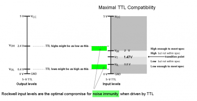
TTL output to Rockwell CPU .png [ 23.15 KiB | Viewed 8405 times ]
Attachment:
File comment: handicapped TTL compatibility
TTL output to WDC CPU .png
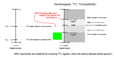
TTL output to WDC CPU .png [ 23.64 KiB | Viewed 8405 times ]

There are also two tiers when we say a certain combination "will work." We need to remember that the TTL-to-WDC combination is far more prone to stop working in noisy circumstances. Those include proximity to external noise, of course, but other important factors include supply noise, crosstalk and inoptimal construction techniques.

The lower of the two attached diagrams shows that the TTL-to-WDC combination actually has negative noise immunity when conveying a 2.4V logic high. Luckily, the shortfall is small when comparing 2.4V with the input transition point, VT. Especially without DC loading, the VOH of most TTL-output devices is likely to exceed the TTL spec of 2.4V... at least sufficiently to bring it slightly above the transition point, and this explains why success is often reported.

But operating near the transition point involves tradeoffs. Poorer noise immunity is the obvious factor, but operating near VT may also increase data setup times, thus degrading the maximum operating speed. :!:

WDC publishes the VIH spec for a reason, and really you want the incoming logic-high level to be at or above VIH. Although VT is only slightly above 2.4V, the shortfall from 2.4V to VIH is not trivial. I suspect there aren't many TTL-output devices which overperform to this extent. This means noise immunity is likely to be compromised, and perhaps maximum clock frequency as well.

I don't feel this unhappy situation deserves to be called TTL compatibility! It is a second-tier solution, not to be confused with the optimal compatibility an engineer would prefer.

-- Jeff

Note: my limited testing of 65xx CPU's can't be used to predict the transition voltage for all extant specimens. Also, the subject of TTL Compatibility involves current as well as voltage, and outputs as well as inputs. But I have focused only on the voltages accepted by CPU inputs because that's by far the most controversial and problematic aspect.

_________________
In 1988 my 65C02 got six new registers and 44 new full-speed instructions!
https://laughtonelectronics.com/Arcana/ ... mmary.html


Last edited by Dr Jefyll on Tue May 11, 2021 8:22 pm, edited 1 time in total.

Top
 Profile  
Reply with quote  
PostPosted: Tue May 11, 2021 5:47 pm 
Offline
User avatar

Joined: Sat Sep 29, 2012 10:15 pm
Posts: 899
Dr Jefyll wrote:
...I don't feel this unhappy situation deserves to be called TTL compatibility! It is a second-tier solution, not to be confused with the optimal compatibility an engineer would prefer.
Agreed. Compatibility implies a 1:1 match between two devices. Perhaps TTL TOLERANT -- it indicates that it is not a happy match. (although that word often implies clamping diodes on a lower-voltage circuit...)

But I hope this topic will not devolve into arguing about the exact meaning of the word 'compatible', or the meaning of the word 'is' for that matter. Focusing on the practical matters:

Obviously the WDC arrangement works in most-likely situations, and as Dr Jefyll pointed out, we are missing a bit of slack if for some reason the valid TTL high is at the low end of acceptable voltage. This puts slightly more pressure on better construction techniques, and trying to eliminate that last bit of ground-bounce.

As for pullup resistors. In most cases of one-offs we won't need them, but it would be nice to know how to build repeatable and noise-tolerant hardware... The cons are:
* reshaping the transition due to capacitance;
* increased power consumption;
* possible back current effects.

I suspect we can get away with very weak pullups, weak enough to ignore the above. Although 10 pullups of even 10K adds up quickly...

_________________
In theory, there is no difference between theory and practice. In practice, there is. ...Jan van de Snepscheut


Last edited by enso on Tue May 11, 2021 6:05 pm, edited 1 time in total.

Top
 Profile  
Reply with quote  
PostPosted: Tue May 11, 2021 5:54 pm 
Offline
User avatar

Joined: Fri Dec 12, 2008 10:40 pm
Posts: 1000
Location: Canada
BigDumbDinosaur wrote:
BillO wrote:
As a exhibit I have attached the datasheet for the ST Micro M27C1001.

'Tis a shame the 27C1001 has become unobtanium. Even my stalwart EPROM, the AMD 27C256-55 has gone the way of $1.00-a-gallon gas. :cry:


True. I still have a small few left and try to buy them when I see them available on eBay. So far I've been able to meet my demands and not gotten any fakes or duds.

_________________
Bill


Top
 Profile  
Reply with quote  
PostPosted: Tue May 11, 2021 7:42 pm 
Offline
User avatar

Joined: Thu Dec 11, 2008 1:28 pm
Posts: 10793
Location: England
It feels to me that if you need pullups to bring a voltage to a reliable level, then that pulling-up is likely to be part of the timing of the machine, and if so, it will matter that the pullup acts quickly enough. (It's also possible that the vulnerable signal is long way off the critical path. So perhaps I'm not saying much...)


Top
 Profile  
Reply with quote  
PostPosted: Tue May 11, 2021 9:58 pm 
Offline
User avatar

Joined: Sat Sep 29, 2012 10:15 pm
Posts: 899
BillO wrote:
...Still not convinced?...


For BillO's worst-case of 400uA:

6) Vd = .0004 x 6500 = 2.6V

7) Vo = 5V – 2.6V = 2.4V, not so nice...

But yeah, I know...

_________________
In theory, there is no difference between theory and practice. In practice, there is. ...Jan van de Snepscheut


Top
 Profile  
Reply with quote  
PostPosted: Tue May 11, 2021 10:51 pm 
Offline
User avatar

Joined: Thu May 28, 2009 9:46 pm
Posts: 8173
Location: Midwestern USA
enso wrote:
As for pullup resistors. In most cases of one-offs we won't need them, but it would be nice to know how to build repeatable and noise-tolerant hardware... The cons are:
* reshaping the transition due to capacitance;
* increased power consumption;
* possible back current effects.

I suspect we can get away with very weak pullups, weak enough to ignore the above. Although 10 pullups of even 10K adds up quickly...

The eight 10K pullups needed to bias a data bus represent only 20 milliwatts of total power consumption, worst-case, in a 5 volt unit. The consumption of the pullups is really not a big deal when compared to a bus transceiver, such as the 74ACT245. A 74ACT245 will consume nearly a watt if all outputs are loaded to the 24mA maximum spec. Given that, if you think you can tolerate the cons enumerated by enso, no reason to not use pullups.

That said, performance with such an arrangement would be better with a much lower value. For example, use of 3.3K on the data bus would consume about 60 milliwatts, worst-case—still less than that of a transceiver seeing maximum loading. The gain is the R-C time-constant would be reduced to one-third of what it would be with 10K pullups, helping to mitigate edge rounding.

Use of a 74xx245 transceiver will exact a penalty in PCB real estate consumption (less so if you are able to use an SOIC package), power consumption and timing. On the plus side, you will get solid drive from rail-to-rail, with no edge rounding, guaranteeing the MPU will not be subjected to marginal input conditions.

Regarding timing and drive, the 74ACT245, 74AHCT245 and 74VHCT245 have single-digit, A-B prop delays. The AHCT and VHCT types will source/sink 8mA, while the ACT245 will source/sink 24mA. All are available in SOIC. The ACT is also available in PDIP for the visually- and/or tactilely-challenged (that would be me :D).

In a 65C02 system, the transceiver's /OE input should be continuously grounded, the DIR (aka TR) input should be directly wired to the MPU's RWB output, and the transceiver's B0-B7 I/O pins should be wired to the MPU's D0-D7 pins. As the state of RWB is established during Ø2 low, the A-B prop delay is the only real timing consideration in this arrangement—unless you qualify chip selects with Ø2 (which is not recommended, and will not work at all with 65xx I/O devices).

In a 65C816 system, the transceiver's DIR input should also be directly wired to the MPU's RWB output. However, /OE should be driven by "Ø1", which is the logical inversion of Ø2. Doing so causes the transceiver to isolate the data bus from the MPU while the latter is emitting A16-A23 on D0-D7. Such an arrangement helps to eliminate a momentary bus contention problem that may arise in some cases.

If your 816 unit's clock generator consists of an oscillator driving a D-type flop and you are using the flop's Q output as Ø2, you can pick up Ø1 from /Q. If you also have a 373/573 latch to demux A16-A23, Ø1 should be connected to the latch's LE input. On the other hand, if Ø2 is derived from an oscillator output instead of a flop, an inverter will be necessary to generate Ø1. That inverter should be very fast to minimize skew between Ø2 and Ø1, which skew can give rise to some obdurate timing problems in a system running at a high Ø2 rate.

_________________
x86?  We ain't got no x86.  We don't NEED no stinking x86!


Top
 Profile  
Reply with quote  
PostPosted: Tue May 11, 2021 11:08 pm 
Offline
User avatar

Joined: Fri Dec 12, 2008 10:40 pm
Posts: 1000
Location: Canada
enso wrote:
BillO wrote:
...Still not convinced?...


For BillO's worst-case of 400uA:

6) Vd = .0004 x 6500 = 2.6V

7) Vo = 5V – 2.6V = 2.4V, not so nice...

But yeah, I know...


Well, that was exactly my starting point .. to determine the worst case internal resistance. So kudos!

_________________
Bill


Last edited by BillO on Tue Jul 05, 2022 1:47 pm, edited 1 time in total.

Top
 Profile  
Reply with quote  
PostPosted: Wed May 12, 2021 12:09 am 
Offline

Joined: Fri Dec 21, 2018 1:05 am
Posts: 1076
Location: Albuquerque NM USA
Pull up resistors are poor substitute for marginal drivers. Let's assume output drivers can only drive to 2.4V and the system relies on pull-up resistors to bring voltage to 3.0V to achieve adequate noise margin. Let's further assume the data bus capacitance is 50pF, so a bit of calculation shows that it takes 130nS for a 10K pull-up to drive 50pF capacitor from 2.4V to 3.0V--not usable unless it is for a very slow system.
Bill


Top
 Profile  
Reply with quote  
PostPosted: Wed May 12, 2021 2:07 am 
Offline
User avatar

Joined: Thu May 28, 2009 9:46 pm
Posts: 8173
Location: Midwestern USA
plasmo wrote:
Pull up resistors are poor substitute for marginal drivers. Let's assume output drivers can only drive to 2.4V and the system relies on pull-up resistors to bring voltage to 3.0V to achieve adequate noise margin. Let's further assume the data bus capacitance is 50pF, so a bit of calculation shows that it takes 130nS for a 10K pull-up to drive 50pF capacitor from 2.4V to 3.0V--not usable unless it is for a very slow system.
Bill

Fortunately, most contemporary devices with TTL outputs can do better than that.

A totem-pole output has a theoretical high limit on a 5 volt system of ~3.5 volts, assuming light to non-existent loading. CMOS inputs are light loads and at least in the opinion of Bill Mensch (see my earlier post), a TTL output should be able to easily attain 3 volts. The threshold at which a 65C02 or 65C816 will recognize a logic 1 on an input is around 2.6 volts, again according to Bill Mensch, and corroborated by Jeff's testing. A 0.4 volt margin over the switching threshold should be more than adequate, assuming the use of good construction techniques.

That being the case, things are not nearly as bleak as they would seem and in fact, most applications in which devices with TTL outputs are connected to WDC MPUs will function fine under reasonable conditions. My POC units are such devices, and POC V1.2 is stable at 20 MHz even whilst I touch the pins on the SRAM—the SRAM has TTL outputs. If there truly was a problem with rise times and noise margins I'd expect the machine to crash when fondling the SRAM. I've not been able to bring that about.

Yes, noise immunity is reduced somewhat, but a lot can be done about that, starting with careful layout and liberal use of bypass capacitors. Substantial ground and Vcc wiring/PCB traces are de rigueur to avoid voltage sags and/or ground bounce. A four-layer board with internal power and ground planes not only solidifies power and ground distribution (and aids in creating a denser layout), it also does a lot to keep a lid on noise and transmission line effects.

If all else fails, there are always bus drivers and transceivers that can act as level converters...

_________________
x86?  We ain't got no x86.  We don't NEED no stinking x86!


Top
 Profile  
Reply with quote  
PostPosted: Tue Jul 05, 2022 4:43 am 
Offline
User avatar

Joined: Fri Aug 30, 2002 1:09 am
Posts: 8430
Location: Southern California
Besides thresholds, I imagine there's a difference in timing, which I'll illustrate this way:
Attachment:
TTL-CMOSthresholdTime.gif
TTL-CMOSthresholdTime.gif [ 14.94 KiB | Viewed 8117 times ]

Note that in this case, the TTL output reaches the TTL threshold before the CMOS output reaches the CMOS threshold, so the TTL part may appear faster; but when it has to drive a CMOS input, it takes it longer to reach the CMOS threshold than the CMOS output takes, because its drive strength is lost before it has charged the bus capacitance up to a high-enough voltage.

This excludes considerations for groundbounce which may make things worse, shifting the input reference level.

_________________
http://WilsonMinesCo.com/ lots of 6502 resources
The "second front page" is http://wilsonminesco.com/links.html .
What's an additional VIA among friends, anyhow?


Top
 Profile  
Reply with quote  
PostPosted: Tue Jul 05, 2022 2:36 pm 
Offline
User avatar

Joined: Fri Dec 12, 2008 10:40 pm
Posts: 1000
Location: Canada
This will never be resolved. Rant follows ..

The simple solution would be to just not use TTL devices with CMOS CPUs. In Jeff's original post he mentioned RAMs, ROMs and PLDs. There may in deed be devices in these classifications that have TTL outputs on them. However I have not ever found one (not that I've gone looking). Anything made from the '80s on would have been made with CMOS technology.

Everyone keeps tripping over the spec sheets. The spec sheets, for whatever reason, give performance in TTL environments. The spec sheets all give output performance into 400uA loads. Why? I guess this is (or was) a reasonable worst case. Your RAM chip might have had to drive a bus with a few TTL loads on it .. back in the day. This is not the case anymore. Today we can all make stuff that has no TTL in it, even using parts from the '80s.

What we can't hope for is that manufacturers will update the spec sheets of obsolete parts. Take them with a grain of salt. A SBC based on a WDC CPU (or other CMOS CPU) using all CMOS components will have loads in the 10s of uA .. maybe 30uA - 60uA (for a big system). Not 400uA!

Even if you did find a TTL RAM or ROM chip, or felt compelled to use a TTL buffer to drive a bus with only CMOS receivers on it, the tiny CMOS loads will mean even these TTL devices will easily meet CMOS input specs.

I would guess that if you have a TTL part that will not drive CMOS input levels into a 50uA load, you have a defective part. It would probably fail entirely trying to drive a 400uA load. Not that you ever have to drive anything new with TTL these days.

_________________
Bill


Top
 Profile  
Reply with quote  
PostPosted: Tue Jul 05, 2022 6:28 pm 
Offline
User avatar

Joined: Fri Aug 30, 2002 1:09 am
Posts: 8430
Location: Southern California
Bill, what I'm thinking of is not the DC drive, but charging the bus capacitance. 400µA charging 50pF only slews at 8mV/ns, meaning 400µA takes 125ns to charge up the 50pF load a single volt. As the TTL-output part starts its trip up from .4V to the higher voltage, it will initially go faster for the first couple of volts because the drive strength is greater; but then it slows way down before it has finished the job of bringing the voltage to a dependable CMOS logic '1'. But yeah, the spec sheets often leave out information we wish they would include, rather than assuming in this case what our intended load is. So although it may work up to some speed, finding the real boundaries requires us to do some very detailed testing which probably none of us has the equipment to do.

_________________
http://WilsonMinesCo.com/ lots of 6502 resources
The "second front page" is http://wilsonminesco.com/links.html .
What's an additional VIA among friends, anyhow?


Top
 Profile  
Reply with quote  
PostPosted: Tue Jul 05, 2022 7:49 pm 
Offline
User avatar

Joined: Fri Dec 12, 2008 10:40 pm
Posts: 1000
Location: Canada
Gotcha.

But I'm really not condoning using TTL in CMOS environments. What I'm really trying to say is those CMOS RAM, ROM and PLD devices we use (and only get TTL load specs for) will do fine in CMOS environments and we need to stop taking those TTL environment specs so seriously because that is just no longer the reality.

_________________
Bill


Top
 Profile  
Reply with quote  
Display posts from previous:  Sort by  
Post new topic Reply to topic  [ 54 posts ]  Go to page Previous  1, 2, 3, 4  Next

All times are UTC


Who is online

Users browsing this forum: No registered users and 9 guests


You cannot post new topics in this forum
You cannot reply to topics in this forum
You cannot edit your posts in this forum
You cannot delete your posts in this forum
You cannot post attachments in this forum

Search for:
Jump to: