6502.org Forum  Projects  Code  Documents  Tools  Forum
It is currently Sat Apr 27, 2024 7:52 pm

All times are UTC


Post new topic Reply to topic  [ 43 posts ]  Go to page Previous  1, 2, 3
Author Message
PostPosted: Fri Jan 26, 2024 5:00 am 
Offline

Joined: Fri Dec 21, 2018 1:05 am
Posts: 1076
Location: Albuquerque NM USA
This 10-second video shows the barebone 6502 bit banging PS2 input and displaying text and video. The PS2 input are captured bit-by-bit during the active video phase by sampling the PS2 data/clock with 31.5KHz interrupts. As many as 8 bytes of PS2 data can be accumulated in a queue during the 15.3mS active video phase. During the 1.4mS vertical retrace phase, the data is read off the queue, decoded, and displayed on screen in 8x15 fonts. The PS2 task also looks for ESC character to toggle the video on or off. The video is BadApple's sword play scene in 192x144 format and stored in the CF disk. It is played at 17 frames/sec when turned on.

The demo video first showed texts entered via PS2 keyboard; then ESC character was entered to turn on the video; more typing and then ESC was entered again to turn off the video.

The horizontal activity bars on the upper right corner of the screen showed the rolling computational loads of last 15 vertical retrace periods. There are 15 horizontal bars, each bar represents how many units of 800-clock (one horizontal sync period) is utilized for that particular vertical retrace period. There are 45 horizontal sync during a vertical retrace and each pixel represents one horizontal sync period. The horizontal bar should not touch the heavy vertical bar at edge of the screen which marks the maximum available throughput.

Most of the throughput was consumed by video display which is moving 1KB of video data from CF disk to display memory every vertical retrace. Processing of PS2 data consumed insignificant amount of throughput. You can barely see a few dimples on the activity bar when keyboard data was entered during the first few seconds of the video.
Bill
Edit, added schematic for pc board and CPLD design
Attachment:
PS2_input_VGA_text_video.gif
PS2_input_VGA_text_video.gif [ 5.11 MiB | Viewed 2573 times ]


Attachments:
VGA65r1n2_CPLD_top_scm.pdf [25.25 KiB]
Downloaded 28 times
VGA65_r1n2_scm.pdf [30.69 KiB]
Downloaded 34 times
Top
 Profile  
Reply with quote  
PostPosted: Sun Jan 28, 2024 4:58 am 
Offline

Joined: Fri Dec 21, 2018 1:05 am
Posts: 1076
Location: Albuquerque NM USA
In addition to reading PS2 keyboard and selecting next row of data to display, I have also added scrolling function in the back porch time slot of the horizontal scan. A scroll variable defines where in video memory to start scanning. By increasing or decreasing the scroll variable, the screen appeared to roll down or up. If video memory is not changed, then it is wrapped around from one end of the screen to the other end. This is fast like the hardware scroll, except it is done in software.

I now have 10 spare clocks left in the back porch time slot, I probably can't add any more functions.
Bill
Attachment:
Scrolling_demo.gif
Scrolling_demo.gif [ 4.32 MiB | Viewed 2531 times ]


Top
 Profile  
Reply with quote  
PostPosted: Sun Jan 28, 2024 3:44 pm 
Offline
User avatar

Joined: Fri Aug 03, 2018 8:52 am
Posts: 745
Location: Germany
you can also pull off horizontal scrolling in a similar fashion by offsetting where in a row of data you start reading from (wrapping around as well), but it would only allow for 8px jumps instead of fine scrolling as you can't do unaligned byte loads without some extra logic.

on another note, i have made my own video card design based on your idea and am almost ready to order the boards. should i make a seperate thread to talk about how it works, or throw it into this one?


Top
 Profile  
Reply with quote  
PostPosted: Sun Jan 28, 2024 4:12 pm 
Offline

Joined: Fri Dec 21, 2018 1:05 am
Posts: 1076
Location: Albuquerque NM USA
I'm packing 3 lines in 256 bytes. Each line is 80 bytes, so there are 16 unused bytes per page that may be somehow useful when doing horizontal scrolling. If picture is in the center with blank field all around, I can do a "fake" horizontal scroll up to 16 bytes, but I don't know how to do it in more general cases.

I've always learn a lot from you designs, so please feel free to describe your approach here.
Bill


Top
 Profile  
Reply with quote  
PostPosted: Mon Jan 29, 2024 6:10 pm 
Offline
User avatar

Joined: Fri Aug 03, 2018 8:52 am
Posts: 745
Location: Germany
plasmo wrote:
I'm packing 3 lines in 256 bytes. Each line is 80 bytes, so there are 16 unused bytes per page that may be somehow useful when doing horizontal scrolling. If picture is in the center with blank field all around, I can do a "fake" horizontal scroll up to 16 bytes, but I don't know how to do it in more general cases.

hmm, sadly you can't make use of the natural wrapping of the Y register because you have multiple lines in a single page. and you have no cycles between reading bytes to do any checks to wrap after n bytes in software.... hmm.

only thing i could think of would be to replace the whole line reading routine, do it with absolute addressing (either X/Y indexed or not) instead of indirect and use self-modifying code to set the addresses to point to the correct bytes.
then you would need to use the small amount of time you have in the H-blanking period to update the addresses to point to the next line and take into account how much the screen is scrolled horizontally. this is obviously a lot more work compared to updating 2 bytes in ZP, but gives you complete horizontal (and vertical) scrolling.

plasmo wrote:
I've always learn a lot from you designs, so please feel free to describe your approach here.

oh boy, this one is gonna be a bit of a doozy.

the main difference to your design is that the CPLD takes care of both H-Sync and V-Sync and there are 2 FIFOs between the CPLD and CPU bus for loading video data.
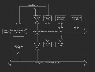
so let's first look at the block diagram i made that roughly describes the system:
Attachment:
draw.io_PtSHM7Wn3g.png
draw.io_PtSHM7Wn3g.png [ 109.79 KiB | Viewed 2478 times ]


Because this is an expansion card to my 65816 SBC (ie the "primary" system) i needed some kind of interface between the it and the 65C02 (ie "secondary" system), so i'm using 2 FIFOs pointing in opposite directions, forming a single bi-directional FIFO. the ATF1502 is only there to handle the decoding logic and FIFO flags on the primary side.

The secondary system has 62kB of RAM (the W24512AK/W241024AK are the fastest DIP SRAM ICs i could find) and 2kB of ROM used for booting and testing. the Interface FIFOs are mapped to memory plus a status and control register which is located inside the CPLD.

let's get to the main part, the 2 FIFOs and the video generation!

the reason why there are 2 FIFOs in parallel is because of the resolution i'm aiming for. specifically 320x240 or 400x300 (currently the logic is designed for 400x300).
as you can probably tell both of these are made using larger resolutions, 640x480 and 800x600 respectively. they're simply divided by 2 both horizontally (drawing each pixel twice in a row) and vertically (drawing each scanline twice in a row). and one important thing to note is that while this quarters the total amount of memory a single frame takes up, it only halves the bandwidth needed to draw it. and the reason why it only havles the bandwidth instead of quartering is because the vertical dividing doesn't actually reduce the amount of scanlines, it only makes 2 consecutive scanlines use the same data. so when drawing 400x300 you actually have to draw all 600 scanlines.

this is where the second FIFO comes in, whenever the CPU reads from the video area in memory the byte is also loaded into both FIFOs, then when the CPLD reads out data to draw on screen, it uses one FIFO for the even scanlines and the other for odd scanlines. this successfully halves the memory bandwidth again, so the CPU only needs to read each byte exactly once per frame.

now let's look at how i plan to keep the FIFOs filled and what happens when the CPU fails to keep them filled.

the FIFOs are all 1kB in size, and i've hooked up their Half-Full Flags (which go LOW when the FIFO is more than half full) through the CPLD, negate it, and then connected to the CPU's IRQ line. so when both FIFOs are less than half full, the CPU will receive and IRQ until they are over half again.
since i'm going for 400x300 @ 1bpp, each line of pixels is 50 Bytes large, therefore when an IRQ occours the CPU knows that it can safely fit 5 whole Rows of data into the FIFOs (5 * 50 = 500, 500 < 512). after which it returns and continues whatever work it did before.
this should work fine and allow the CPU to do regular work while only occasionally being interrupted to top off the FIFO.

but i still nedded a plan in case the CPU gets stuck in an infinite loop with interrupts disabled and atleast one of the FIFOs actually runs dry. if that happens the video output disables itself and sends an NMI to the CPU. the CPU can then manually reset the FIFOs (emptying them) and reset the IRQ variables back to the beginining of the frame data and preloads 10 lines of data into the FIFOs before re-enabling the video output again.
enabling the video output doesn't make it continue drawing right away, that would be stupid as the CPU has no idea where the video output currently (like in the middle of a frame) so instead at the end of each frame the video output checks the enable bit in the control register and only then reenables itself, so that the data in the FIFOs lines up with the start of the next frame.

on another note, the FIFOs are always active, even during H- and V-Blank. this is required since the FIFOs could hit the 50% threshold at any time, so the CPU needs to be able to have data loaded into them at any time as well.
but this creates an issue where the CPU wouldn't be able to actually access the data when trying to modify it without a copy of the data also landing in the FIFOs. so to get around that issue i designated 2 seperate video areas. one is always the active area, accessing it will cause writes to the FIFOs while the other one just behaves like regular memory.
so the CPU would be accessing the active area to draw it to the screen, and use the inactive area to construct the next frame, then when it's done it will write to a bit in the control register to flip them (the change only applies at the end of the current frame) and then repeat the process.
one downside is that you don't get access to the current frame to draw the next one.

an alternative idea i had would be to replace that control bit with an enable bit for the FIFO writes. and only enable them at the start of the IRQ ISR and then disable them again before RTI-ing. this would free up ~16kB of RAM and allow the drawing code to directly access it, but could introduce artifacts while drawing stuff to the screen.

and on a final note, since the video circuit is only connected to the CPU bus via some async FIFOs, the CPU and video side don't have to share the same clock. i could run the video side at 40MHz (20MHz pixel clock) and run the CPU at 25MHz to get even more performance, or in case it cannot handle that speed, 16MHz and just spend a bit more time per frame filling up the FIFOs. i have also included a small resistor DAC connected to RGB in parallel to allow for 4 shades of black/white in case i want to go for a higher color depth.

.

but yea that's around the idea i had for this. it's obviously a lot more complicated and relies more on hardware to free up CPU time (i could even fit a small DMAC into the CPLD as it's only around ~50% full, and free up even more CPU time!) but since i wanted to use this as a Co-Processor to do things like drawing shapes and text, i thought that i should free up as much CPU time as possible. maybe i can even get Bad Apple running?

anyways, if there are any more questions just ask! maybe i can even answer them :lol:


Top
 Profile  
Reply with quote  
PostPosted: Mon Jan 29, 2024 10:21 pm 
Offline

Joined: Fri Dec 21, 2018 1:05 am
Posts: 1076
Location: Albuquerque NM USA
A few thoughts as I read your post:
* 720x FIFO has a re-transmit input. Can it be used to send data twice?
* The 39SF0x0 ROM is not necessary. You can either have a small ROM in CPLD and bootstrap from FIFO or more interestingly, immediately after reset wire 6502's RDY to FIFO_empty and execute instruction stream that's loaded into FIFO by 65816.
* Not only can it do pan and scroll, it seems to me power-of-2 digital zoom may also be possible.
* Video FIFO decoupled the 6502 so I think it has more freedom to do things like audio, I2C, and PS2 keyboard interface.
* FIFO and RAM are all fast, so you should run this as fast as you can. 30MHz 6502 is probably realistic.
Bill


Top
 Profile  
Reply with quote  
PostPosted: Mon Jan 29, 2024 11:01 pm 
Offline
User avatar

Joined: Fri Aug 03, 2018 8:52 am
Posts: 745
Location: Germany
i was just about to go to bed, but i still have some time to answer
plasmo wrote:
720x FIFO has a re-transmit input. Can it be used to send data twice?

kind of, but also not really... the re-transmit input only sets the read pointer back to 0. so you could have the CPU write a row of pixels to the FIFOs, have the video circuit read the data for the first scanline, trigger the retransmit, then read the same data again for the second scanline.
but after that you have to reset the FIFOs completely and then load the next row of pixels into it, otherwise the re-transmit won't work. this basically shrink's the FIFO's usable size down to a single row of pixels, wasting the rest. plus the CPU would need to fill the FIFO up more often (every second scanline) but it is certainly an option if you want to reduce the IC count.

plasmo wrote:
The 39SF0x0 ROM is not necessary. You can either have a small ROM in CPLD and bootstrap from FIFO or more interestingly, immediately after reset wire 6502's RDY to FIFO_empty and execute instruction stream that's loaded into FIFO by 65816.

i did try to use a small ROM inside a CPLD last time and it didn't work, so i thought "screw it i'll just use a normal ROM this time to be safe", as i mainly just want the secondary CPU to work and do some test communication to the primary system. also RDY/BE are connetced to the ATF1508 so i could directly execute from the FIFO if i change the logic a bit, i might try that once i have the boards.

plasmo wrote:
Not only can it do pan and scroll, it seems to me power-of-2 digital zoom may also be possible.

what exactly do you mean? your system or mine? either way not sure how you would pull of pixel based scrolling/zooming...

plasmo wrote:
Video FIFO decoupled the 6502 so I think it has more freedom to do things like audio, I2C, and PS2 keyboard interface.

yea i guess it could be used as a "Super IO" Card, if this one works i might try another one with a 65C22 onboard for software SPI and PS/2 (maybe even use 65C816 with a W241024AK, which are 128kB, so i could try 320x200 @ 8bpp (64000 Bytes) in bank 1 and leave bank 0 free for the CPU). and if my math is a right a 25MHz 65816 should just about be able to handle that memory bandwidth, but those are dreams for another time!

plasmo wrote:
FIFO and RAM are all fast, so you should run this as fast as you can. 30MHz 6502 is probably realistic.

the FIFOs i got have an access time of 25ns (plus whatever propagation delay the CPLD has), so even at 20MHz i already need to add 1 wait state on the 65C02 side for them to function properly. plus the board is rather large and only 2-layer so i'm not sure if i can even reach 25MHz, let alone 30MHz. but if i can pull it off i would have a ton of CPU time, might even try to do some 3D math!

.

anyways it's really late here i should go to bed...


Top
 Profile  
Reply with quote  
PostPosted: Sat Feb 10, 2024 5:48 pm 
Offline

Joined: Fri Dec 21, 2018 1:05 am
Posts: 1076
Location: Albuquerque NM USA
I forgot it is Chinese New Year and JLCPCB is shut down for a while, so my current batch of boards will be delayed. Therefore I'm returning to 6502-based VGA controller (VGA65) project for a while.

Software for VGA65 was going slowly. PS2 keyboard and scrolling functions are working well, so I was working on a basic monitor that can display and modify memory and go execute software at specified address. The monitor functions must be done in the vertical retrace period and texts must be render from font table so it took longer to execute a command which may require multiple vertical retrace periods to complete. Never have done re-entrant software for 6502 and it certainly was a learning experience.

Because vertical sync is under software control, the penalty of software execution longer than vertical retrace period is loss of video sync which needs a couple second to re-sync. Very annoying.

I didn't think 64-macrocell CPLD has enough resources to do a complete video hsync/vsync generation, but I was surprised! I was able to cram 10-bit horizontal 800-pixel counter with associated horizontal sync and 10-bit 525-line counter with associated vertical sync in the CPLD. Beside the pixel shifter, horizontal pixel counter and sync, vertical line counter and sync, this metaphorically bulging CPLD also contain CF disk boot ROM, CF interface, serial port, PS2 interface, RAM bank, and RAM enable, all in a 64-macrocell PLCC44 package. It is really quite astonishing.

With video syncs generated in hardware, the VGA monitor will always be in sync. So if a command took too long to execute, it will spill into next video frame and momentarily trash the display but without loss of sync; it is like flickers or "snow" on screen. In fact, I can run memory diagnostic on the video memory and see constantly changing random patterns, but no loss of video sync.

It is still desirable to do commands within the vertical retrace period, but certain commands like serial file load may trash the screen for the duration of the command. That's tolerable.
Bill


Top
 Profile  
Reply with quote  
PostPosted: Sun Feb 25, 2024 4:30 pm 
Offline
User avatar

Joined: Fri Aug 03, 2018 8:52 am
Posts: 745
Location: Germany
Alright, my PCBs arrived! this was the fastest one yet, JLC send them at the start of the week and they arrived yesterday.
and while my Amiga 500 still doesn't have functional IDE despite the 4 PCBs i've made for it at this point, i can atleast say that the video card is coming along nicely!
Attachment:
20240224_182713.jpg
20240224_182713.jpg [ 2.74 MiB | Viewed 2364 times ]


For testing purposes the 1508 only contains the logic necessary for the 65C02 to function, because i of course first want to make sure the System works at all before throwing video generation at it.

4kB of ROM, 60kB of RAM, and 2 Bytes of IO for the Status/Control Register and the Bi-Directional FIFO for interfacing. I'm currently running it with a 25MHz clock divided by 4 for a 6.25MHz CPU clock. the current ROM program just waits for a byte in the FIFO, reads it, inverts all the bits, and then sends it back.
and it runs perfectly fine with no botch wires (yet)!

next i want to try running at some faster clock speeds (12.5, 20, 25MHz) with wait states for IO and ROM, then i can think about adding video.
even if the video stuff doesn't work as planned i would still have a fast Co-Processor for offloading computational work to.

I'll throw out an update when i got something more complex going


Top
 Profile  
Reply with quote  
PostPosted: Wed Feb 28, 2024 8:52 pm 
Offline
User avatar

Joined: Fri Aug 03, 2018 8:52 am
Posts: 745
Location: Germany
well then. i was just kinda watching anime and eating dinner and checking the forum from time to time, almost making myself ready for bed when i saw plasmo's post over on the >8MHz thread asking about the issues i was having.

then i thought, well damn, might as well try myself at this again for like an hour and see if i can figure out the cause and make a small update in this thread about how inconsistent the FIFO interface was and what i tried so far.
i did some more program tests and wrote up a post, but then out of nowhere i actually freaking fixed it! this was not expected at all!

so i now deleted that post and re-wrote it from scratch to just say what it was.

basically the issue i was having was just the interface behaving weirdly, it would send extra bytes when not asked to and misread bytes i would send it. i triple checked the schematic, swapped out the FIFO chips, redid my code on both sides... nothing was working.
so then i checked quartus to compare the pin assignement to the schematic and then i noticed it...
i renamed 2 pins in the logic which were for the FIFO interface, the full flag (when the transmitting FIFO is full it's 1) and the empty flag (when the receiving FIFO is empty it's 1). and after renaming them i forgot to reassign them to their pins, so the fitter assigned them automatically. the CPLD is completely full so the only free pins left were the 2 for the flags, but the fitter assigned them swapped. so when the CPU read out the full flag it actually read the empty flag, and vise versa.

so i swapped them by manually assigning them, reflashed the CPLD and now it works perfectly!
i won't be testing RAM yet since it's pretty late. but tomorrow i want to implement a small bootloader on the ROM to load a program from the FIFO to memory and then execute it (with 0 wait states) which should allow me to test some higher speeds!


Top
 Profile  
Reply with quote  
PostPosted: Thu Feb 29, 2024 6:52 pm 
Offline
User avatar

Joined: Fri Aug 03, 2018 8:52 am
Posts: 745
Location: Germany
another smol update. i made the bootloader and tested it at various speeds, even using my DS1086 board to program it while in circuit without having to power cycle the whole thing.

~25MHz seems to be the upper limit. at higher speeds (even just 26MHz) it can still load a program into RAM (because the ROM slows the clock down) but as soon as it tries to execute the function (at 0 wait states) it fails and seems to completely crash.
currently i'm using a 25MHz Oscillator to run the CPU with 1 wait state on both ROM and the FIFOs.

on another note, i guess because the data paths are a lot shorter on my current VGA compared to the last i'm atcually able to run the SBC itself slightly faster as well. using the DS1086 again i got up to 35MHz (17.5MHz CPU clock, before it was 15MHz), pretty good!

i guess next goal is actually setting up the VGA logic, the current design takes up around 28 Macrocells (22%) so i should have enough room to get something working.


Top
 Profile  
Reply with quote  
PostPosted: Fri Mar 01, 2024 2:58 pm 
Offline

Joined: Fri Dec 21, 2018 1:05 am
Posts: 1076
Location: Albuquerque NM USA
This is the PC board version of VGA65 (2-layer PCB, 100mmX100mm). It boots from CF disk, loads file via serial port at 115200, has monochrome 640x480 VGA graphic interface and PS2 keyboard interface. W65C02 is operating at 25.175MHz and has two banks of RAM. This is a minimal standalone 6502 computer and still has prototype area for more experimentation.

I'm currently working on a monitor for the board that has basic functions of display memory, modify memory and execute program.
Bill
Attachment:
VGA65_rev0PCB.jpg
VGA65_rev0PCB.jpg [ 1.15 MiB | Viewed 2276 times ]


Top
 Profile  
Reply with quote  
PostPosted: Sat Mar 02, 2024 3:40 am 
Offline

Joined: Fri Dec 21, 2018 1:05 am
Posts: 1076
Location: Albuquerque NM USA
Here is a screen capture of a basic monitor program for above VGA65 hardware. It takes input from PS2 keyboard and output to 640x480 monochrome VGA monitor. The simple monitor can change memory, display memory, and go execute program. It also has a BadApple demo.

VGA65 is a graphic display with 6502 as the graphic controller so it spent most (90%) of its time painting the VGA screen; monitor functions are performed during the vertical retrace period which is not enough time to display multiple lines of data because texts need to be rendered from 8x15 fonts. Each vertical retrace period only has enough time to scroll the screen and display one new line. The 15-bar display at the right side of screen measures how much time is utilized. I had struggled writing this simple monitor; a real time scheduler would be very helpful here.

Ironically, it can display graphic image much faster. The BadApple demo is stored in CF disk; it can be retrieved from CF disk and displayed on screen as 192x144 video at 17 frames a second.

The noise at the bottom of screen is due to lack of vertical blanking. The CPLD is completely full so to add the vertical blanking logic, I'll need to re-assign most of the CPLD pins. That'll be next iteration of PC board. For now, I just adjust the monitor to hide the noise.
Bill
Attachment:
VGA65_monitor_plus_badapple_demo.gif
VGA65_monitor_plus_badapple_demo.gif [ 5.1 MiB | Viewed 2251 times ]


Top
 Profile  
Reply with quote  
Display posts from previous:  Sort by  
Post new topic Reply to topic  [ 43 posts ]  Go to page Previous  1, 2, 3

All times are UTC


Who is online

Users browsing this forum: No registered users and 34 guests


You cannot post new topics in this forum
You cannot reply to topics in this forum
You cannot edit your posts in this forum
You cannot delete your posts in this forum
You cannot post attachments in this forum

Search for:
Jump to: