6502.org Forum  Projects  Code  Documents  Tools  Forum
It is currently Mon May 06, 2024 5:36 pm

All times are UTC


Post new topic Reply to topic  [ 182 posts ]  Go to page Previous  1, 2, 3, 4, 5, 6 ... 13  Next
Author Message
PostPosted: Wed Sep 30, 2020 6:41 am 
Offline
User avatar

Joined: Sun Oct 18, 2015 11:02 pm
Posts: 428
Location: Toronto, ON
Dr Jefyll wrote:
Drass wrote:
(I didn’t have another AND gate, so I used an XOR gate and tied one of the inputs to GND with a little patch cable. It’s a mess but it did the job). :D
Urk! This description and the photo you posted are creating, how shall I say, an unsettled reaction in my tummy (!). But I won't argue with success -- nice work, Drass! :P
Thanks Jeff. To be clear, the AND gate has one input tied to VCC and the XOR gate one input tied to GND. Each passes the remaining input unchanged and the drivers always add up. There is no effect on the logic value of the input but the delay is properly reflected.

Quote:
In case anyone has forgotten how darn small these gates are, have a look at the photo upthread. :shock:
Yeah, that XOR gate is 0.65mm pitch, so the jumper spans 1.3mm from pin 1 to pin 3 while carefully avoiding pin 2. :evil:

_________________
C74-6502 Website: https://c74project.com


Top
 Profile  
Reply with quote  
PostPosted: Wed Sep 30, 2020 7:56 am 
Offline
User avatar

Joined: Fri Nov 09, 2012 5:54 pm
Posts: 1393
Drass and Jeff: putting CMOS output in parallel, nice going.
//I still wonder if clock buffers/distributors could distribute data signals as well... and if their outputs could be wired together.

:---

Now for some boring statistics: Fairchild\Onsemi NC7SV versus TI 74AUC.
Propagation delays of different logic chips, load = 30pF parallel 500 Ohms to GND, 25°C.

Format is "min. / typ. / max." in ns.
When typ. was not specified, I assumed typ. = (min. + max.) /2 and added a question mark.

//1 gate per chip
NC7SV08: 2.3V..2.7V: 0.8 / 1.2 / 2.6, 2.7V..3.6V: 0.7 / 1.0 / 2.3
NC7SV14: 2.3V..2.7V: 0.8 / 1.8 / 3.7, 2.7V..3.6V: 0.7 / 1.5 / 3.3
NC7SV86: 2.3V..2.7V: 0.8 / 1.2 / 3.6, 2.7V..3.6V: 0.7 / 1.0 / 3.3

//1 gate per chip
74AUC1G08: 2.5V: 0.5 / 1.25? / 2.0
74AUC1G14: 2.5V: 0.5 / 1.5? / 2.5
74AUC1G86: 2.5V: 0.7 / 1.35? / 2.0

//2 gates per chip
74AUC2G08: 2.5V: 1.0 / 1.3? / 1.6
74AUC2G14: not available.
74AUC2G86: 2.5V: 0.7 / 1.35? / 2.0

//4 gates per chip
74AUC08: 2.5V: 0.5 / 1.15? / 1.8
74AUC14: 2.5V: 0.7 / 1.7? / 2.7
74ACU86: not available.

;---

Sorted for speed, based on typ. propagation delay:
NC7SV08@3.3V:1.0 > 74AUC08:1.15? > NC7SV08@2.5V:1.2 > 74AUC1G08:1.25? > 74AUC2G08:1.3?
NC7SV14@3.3V:1.5 = 74AUC1G14:1.5? > 74AUC14:1.7? > NC7SV14@2.5V:1.8 //74AUC2G14 not available.
NC7SV86@3.3V:1.0 > NC7SV86@2.5V:1.2 > 74AUC1G86:1.35? = 74AUC2G86:1.35? //74AUC86 not available.

And the winner for Schmitt trigger inverters, AND and XOR is +3.3V powered NC7SV.

;---

Edit:
Requested by Jeff down in the thread:

NC7SV04@3.3V: 0.7 / 1.5 / 2.3
NC7SV04@2.5: 0.8 / 1.8 / 2.7
74AUC1G04: 0.5 / 1.2? / 1.9
74AUC2G04: 0.7 / 1.1? / 1.5
74AUC04: 0.5 / 1.25? / 2.0

NC7SV240: not available.
74AUC1G240: 0.8 / 1.25? / 1.7
74AUC2G240: 0.6 / 1.15? / 1.7
74AUC240: 0.9 / 1.25? / 1.6
74AUCH240: 0.9 / 1.25? / 1.6

The winner for inverters is +2.5V powered 74AUC2G04.

Attachment:
cmos_propagationdelay.png
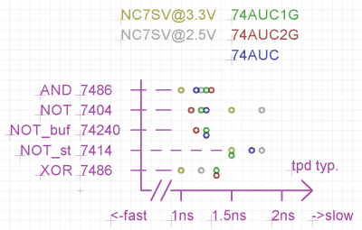
cmos_propagationdelay.png [ 48.22 KiB | Viewed 2379 times ]

;---

Just for the fun of it:

//-5.2V NECL from the 80s (obsolete):
//MC10H113 (4* XOR): 0.40 / 1.05? / 1.70
//MC10H104 (4* AND): 0.45 / 1.10? / 1.75

//fully differential 3.3V..5V PECL with chips from 2020:
//MC100EP05 (1* AND): 170ps / 220ps / 270ps
//MC100EP08 (1* XOR): 180ps / 250ps / 300ps

//CML and "don't look for the price": AnalogDevices.
//HMC726 (1*AND): 95ps typ. //13 Gbps
//HMC725 (1*XOR): 105ps typ. //13 Gbps

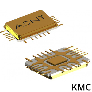
//CML and IDKFA: Adsantec, the computer probably would be as expensive as a Cray-1 then.
//ASNT5160 (1* AND): 50 Gbps, 25GHz
//ASNT5143 (1* XOR): 32 GHz

Attachment:
adsantec_package.png
adsantec_package.png [ 78.3 KiB | Viewed 2455 times ]


Last edited by ttlworks on Wed Oct 07, 2020 6:34 am, edited 2 times in total.

Top
 Profile  
Reply with quote  
PostPosted: Wed Sep 30, 2020 9:35 am 
Offline
User avatar

Joined: Fri Nov 09, 2012 5:54 pm
Posts: 1393
Analog FET switches.

There are switches for USB3.0, analog video, DisplayPort (DVI\HDMI), PCI_Express, Gigabit Ethernet, MIPI M-PHY and whatnot.
While them switches are designed to feed through high frequencies, the typical switching time between the channels seems to be slower than for our humble 74AUC2G53.

For instance: TI TS3L4829 Gigabit LAN switch. Propagation delay 40ps typ., but select time 0.5ns .. 15ns.
74AUC2G53: propagation delay 100ps max., select time 0.5ns .. 1.6ns. //Edit: 500Ohm, 15pF load to GND.

Found no faster chip than the 74AUC2G53 in the NC7* or 74* logic families, so it looks like we have to stick with it.

74AUC2G53:
Supply voltage: VCC Maximum ratings -0.5V .. 3.6V, recommended "operates at 0.8V .. 2.7V".
Input voltage range (A and INH ?): Maximum ratings -0.5V .. 3.6V, recommended 0V .. 3.6V.
Switch I\O voltage range: Maximum ratings -0.5V .. VCC+0.5V, recommended 0V .. VCC.

Translation:
If VCC = 3.3V, 74AUC2G53 won't get damaged by VCC. Chip might be working at VCC = 3.3V, but TI won't take any responsibility for this.
If VCC = 2.5V, driving the select input A with 3.3V is supposed to work, but thou shalt not send more than 2.5V into the switch.


Last edited by ttlworks on Thu Oct 01, 2020 1:05 pm, edited 1 time in total.

Top
 Profile  
Reply with quote  
PostPosted: Wed Sep 30, 2020 2:03 pm 
Offline
User avatar

Joined: Fri Nov 09, 2012 5:54 pm
Posts: 1393
For SBC (Q = A - B), we would have to invert one of the ALU adder inputs.
Drass's idea was putting XOR gates between RAM data output and ALU B latch input.

;---

A nice idea would have been hiding that part in the pipeline by wiring two registers with three_state outputs in parallel:
one with non_inverting outputs, one with inverting outputs... replacing the ALU B latch.

The fastest register with inverting three_state outputs I was able to find is the 74AC534,
propagation delay is 2.5ns .. 16ns at 3.3V, that's way too slow.

//74ABT534 propagation delay is 3.4ns .. 6.7ns, but it's 5V only, and it's still way too slow.

;---

Noticed that there is a buffer containing 8 XOR gates (the chip has a control pin for inverting or non_inverting a Byte):
In theory the 74AHC8541 could simplify the PCB layout,
propagation delay is 15ns typ. at 3.3V, that's way too slow.

Was unable to find a chip with that functionality in logic families other than 74AHC.


Last edited by ttlworks on Thu Oct 01, 2020 6:13 am, edited 1 time in total.

Top
 Profile  
Reply with quote  
PostPosted: Wed Sep 30, 2020 7:15 pm 
Offline
User avatar

Joined: Fri Dec 11, 2009 3:50 pm
Posts: 3353
Location: Ontario, Canada
ttlworks wrote:
//I still wonder if clock buffers/distributors could distribute data signals as well... and if their outputs could be wired together.
Ordinarily there'd never be a need to wire their outputs together, so do you have something special in mind, Dieter? Like replacing our doubled-up gate, perhaps? :)

ttlworks wrote:
Now for some boring statistics: Fairchild\Onsemi NC7SV versus TI 74AUC.
Nice work! I particularly like the graph.

One thing that really jumps out is the laggardly performance of the inverters with Schmitt trigger ( NOT_st ). It would be helpful if you could expand the graph to include inverters without Schmitt trigger. I expect these will be substantially faster... and, in an actual CPU, a non-Schmitt inverter ought to suffice. :!:

(It won't suffice for the test PCB, of course. Attentive readers will notice there's a DC feedback path from the inverter's output back to its input... meaning that a non-Schmitt inverter would eventually go linear and self-bias to roughly 50% of Vcc).

-- Jeff

PS to Drass: yes, of course you're right: the output of the AND expresses the same logical equation as the output of the XOR you soldered on top. However, I have a fuss-budget streak that makes me nervous about any timing skew between the two nominally identical outputs. Since the dice are non-identical there may indeed be a little bit of skew, and since the outputs are in parallel skew translates to current spikes, and this makes me a bit queasy. But, in the heat of the night when the solder is flowing, anything goes!! :twisted: :lol:

_________________
In 1988 my 65C02 got six new registers and 44 new full-speed instructions!
https://laughtonelectronics.com/Arcana/ ... mmary.html


Top
 Profile  
Reply with quote  
PostPosted: Thu Oct 01, 2020 6:20 am 
Offline
User avatar

Joined: Fri Nov 09, 2012 5:54 pm
Posts: 1393
Dr Jefyll wrote:
Ordinarily there'd never be a need to wire their outputs together, so do you have something special in mind, Dieter? Like replacing our doubled-up gate, perhaps? :)

No, replacing the ALU B latch with two latches (inverting plus non_inverting) to get rid of the XOR gates in front of the ALU B latch inputs.
Looks like this didn't come out that clear from my posting above, so I felt the need to clarify/edit my text.

Dr Jefyll wrote:
It would be helpful if you could expand the graph to include inverters without Schmitt trigger.

Done, the fastest 7404 type inverter appears to be 74AUC2G04.

Dr Jefyll wrote:
However, I have a fuss-budget streak that makes me nervous about any timing skew between the two nominally identical outputs.

Yes, that's the reason for my asking if clock buffers could distribute a data signal instead of a symmetrical clock signal. :lol:
Skew between the outputs of clock buffers is supposed to be less than skew between the outputs of logic gates.

There are clock buffers with two inputs and a multiplexer switching between the inputs, like LMK0334.
Here, the interesting question is whether the multiplexer switches asynchronously according to the CLKin_SEL control signals or not.
If it switches asynchronously, it would be interesting to know if the chip probably could be used as a two input logic gate with 4 outputs that could be wired together.
Propagation delay ca. 1.5ns typ., but maybe there are faster chips...

//'True art' is using components\parts in a way not predicted/intended by their manufacturer.
Edit: I miss the good old times, when Fairchild datasheets had contained the transistor level equivalent of a chip.


Top
 Profile  
Reply with quote  
PostPosted: Thu Oct 01, 2020 12:05 pm 
Offline
User avatar

Joined: Sun Oct 18, 2015 11:02 pm
Posts: 428
Location: Toronto, ON
Dr Jefyll wrote:
But, in the heat of the night when the solder is flowing, anything goes!! :twisted: :lol:
Indeed, you‘ll be amused to learn that I had an AND gate but lost it after a false move sent it pinging around the PCB like a pinball. It was my last one, so an XOR gate it had to be! :)

ttlworks wrote:
Now for some boring statistics: Fairchild\Onsemi NC7SV versus TI 74AUC.
Thanks for this analysis Dieter. It’s going to be valuable to have these various tradeoffs available when the time comes.

I like the 3.3V NC7SV family, and indeed I based my original cycle-time estimates on it (along with AVC and LVC). It doesn’t have the same dynamic impedance outputs (DOC) that the AUC and AVC families have, so longer traces will require termination. However, that won’t be the case in close proximity sub-circuits like the adder where their stronger drive (24mA) make them a great choice for the carry chain.

It’s worth noting the mixed supply environment we’re seeing here. We will want to keep ICs powered optimally for maximum speed and the CPU will need counters, decoders and muxes that are only available in the 3.3V LVC and CBTLV families. The AVC and AUC families are both great choices for registers at 3.3V and 2.5V respectively, so there is some flexibility there. But there seems to be no good 3.3V alternative to the 74AUC2G53 FET switches in the adder. (Most AUC ICs are 3.3V tolerant, but as you correctly point out, the 74AUC2G53 does not want voltages in excess of VCC on its data pin. This may impose some restrictions on the ICs that drive them and perhaps also a mixed supply requirement).

A related issue is how best to keep the VCC place as continuous as possible. From what I understand, a split in the VCC plane will disturb the impedance of traces running across it, and create loops in the return currents with added inductance. I have been thinking in terms of distinct 3.3V and 2.5V “zones” in the VCC plane with stitching caps between the split planes to create a more direct path for return currents. I’m not sure what impact these discontinuities will have on 100MHz signals, but I suspect we will want to avoid a unnecessarily checkered VCC plane.

So, all that to say that will want to give some thought to the various supply levels and how best to manage them on the PCB. I suspect it will be possible to keep mostly to a 3.3V supply (using LVC, AVC and CBTLV families), and use 2.5V in specific circuits (like 74AUC2G53s in the adder, for example). But perhaps I am being unnecessarily cautious here and a more liberal distribution of various supply voltages on the board is not a problem. I’m not sure.

P.S. Perhaps a 74CBTLV3126 and 74CBTLV3125 pair can be used as a 3.3V alternative to a 74AUC2G53 in the FET carry chain?

_________________
C74-6502 Website: https://c74project.com


Top
 Profile  
Reply with quote  
PostPosted: Thu Oct 01, 2020 1:04 pm 
Offline
User avatar

Joined: Fri Nov 09, 2012 5:54 pm
Posts: 1393
Drass wrote:
Perhaps a 74CBTLV3126 and 74CBTLV3125 pair can be used as a 3.3V alternative to a 74AUC2G53 in the FET carry chain?

Short answer: No, I don't think so.
Long answer:

//Load: 500Ohm, 50pF to GND
74CBTLV3125@3.3V: tpd=250ps max., ten= 2.0 / 3.2? / 4.4, tdis= 1.0 / 2.6?/ 4.2
74CBTLV3126@3.3V: tpd=250ps max., ten= 1.9 / 3.05? / 4.2, tdis= 1.0 / 2.9?/ 4.8

//Load: 500Ohm, 30pF to GND
74CBTLV3125@2.5V: tpd=150ps max., ten= 2.0 / 3.3? / 4.6, tdis= 1.1 / 2.5? / 3.9
74CBTLV3126@2.5V: tpd=150ps max., ten= 1.6 / 3.05? / 4.5, tdis= 1.3 / 3.0? / 4.7

When using 74CBTLV3125 plus 74CBTLV126, the switching times for both chips don't exactly match.
I think that capacitance per switch is 7pf typ, that's 14pf typ. for two switches wired together.

;---

//Load: 500Ohm, 30pF to GND
74AUC2G53@2.5V: tpd=200ps max., switching time is 0.5 / 1.4? / 2.3
I think that the capacitance per switch is 4.5pF.

;---

Conclusion:
Compared to 74CBTLV3125\74CBTLV3126, 74AUC2G53 has a slightly slower propagation delay, but switches faster, and gives you a lot less capacitance per node (and a nicer PCB layout).
Would suggest to stick with 74AUC2G53.

To answer your next question:
//Load: 500Ohm, 30pF to GND
74AUC1G125: tpd= 0.9ns .. 1.7ns
74AUC2G125: tpd= 0.7ns .. 1.8ns
74AUC125: tpd= 0.5ns .. 2.1ns

That's way too slow, didn't bother with looking at 74AUC*126.


Top
 Profile  
Reply with quote  
PostPosted: Sat Oct 03, 2020 7:34 pm 
Offline
User avatar

Joined: Sun Oct 18, 2015 11:02 pm
Posts: 428
Location: Toronto, ON
Thanks for those figures Dieter. I agree we should stick with the 74AUC2G53.

Alright, time for an update ...

I had a chance to run the 16-bit FET incrementer test. I first tried a 16-bit FET carry chain in series just to see what kind of delay we might see. (For reference the test board is configured as follows: R2, R4, R5, R9, R11, R12, R14 and R8 are open and R1, R3, R6, R7, R10, R13 and R15 are closed .. schematic here). Here are the results:

@ 2.5V, 2.2MHz ==> 14.2ns
@ 2.7V, 2.4MHz ==> 12.9ns
@ 2.8V, 2.5MHz ==> 12.5ns
@ 3.3V, 2.9MHz ==> 10.7ns

As expected, a serial 16-bit FET carry chain is much too slow. The incrementer result in the CPU will be fed directly to the synch RAM (when incrementing PC for example), so the setup time of 1.5ns applies here as well. Add to that the tpd for the source register, some transit time, clock skew, etc. and we're pretty much left with about 6.5ns for the incrementer (just like with the adder).

So, the next step was to try carry lookahead. Four levels of AND gates on this board simulate carry lookahead for the first 12 bits of the incrementer. In the test circuit, the lookahead carry is then fed to four FET switches to simulate incrementing the final four bits. In this case, we don't have to include the switch time in the circuit since that happens concurrently with the carry lookahead.

So, I configured the board accordingly (as above, except that R13 is moved to R12 and R15 is moved to R14) and ran the test. Here are the results:

@ 2.5V, 4.9MHz ==> 6.4ns
@ 2.7V, 5.2MHz ==> 6.0ns
@ 2.8V, 5.4MHz ==> 5.8ns
@ 3.3V, 5.9MHz ==> 5.3ns

All good results! -- so we now know we can make a 16-bit incrementer that will be fast enough. Happy day. :)

I then thought I would go back and clean up the 8-bit adder. Recall that I had doubled by drive into the carry chain by soldering and XOR gate on top of the AND gate at the start of the chain, giving Jeff some vertigo. I remembered the previous version of the test board had an NC7SV08 gate on it, so I pulled it off and used it in place of the 74AUC1G08 to drive the carry chain on the new board. The ICs have exactly the same pinout so the footprint would work fine. The NC7SV family chips are rated at 3.3V, so running it at 2.5V would be a little slower. However, the greater drive might well compensate for that.

Alright, I fired up the test at 2.5V with the NC7SV08 in place in the new 8-bit adder, and here is what I got:

@ 2.5V, 4.94MHz ==> 6.33ns

Bingo! it's confirmed. NC7SV logic is a better choice to drive the carry chain. It can be used conveniently for all the AND gates along the carry chain to provide the additional drive when needed. There is also an NC7SV74 flip-flop available which will do nicely for the ALU input Carry. :)

Cheers for now,
Drass

P.S. The four carry lookahead AND gates are on a single VQFN 74AUC08 IC. So, yes, soldering the VQFN package worked out just fine! That’s going to come in handy when it’s time to do layout.


Attachments:
0CA8FED0-C140-4E70-8573-9605C41B46AA.jpeg
0CA8FED0-C140-4E70-8573-9605C41B46AA.jpeg [ 153.06 KiB | Viewed 2287 times ]

_________________
C74-6502 Website: https://c74project.com
Top
 Profile  
Reply with quote  
PostPosted: Sun Oct 04, 2020 5:41 am 
Offline
User avatar

Joined: Thu Apr 11, 2019 7:22 am
Posts: 40
Hi Drass,

Quote:
Four levels of AND gates on this board simulate carry lookahead for the first 12 bits of the incrementer
please, can you clarify that for me?. I see you are using 4 'and' gates in series to simulate a carry look ahead delay, then you apply that delay to a 4 bit FET switch incrementer. So if I got it right, you are simply testing a 'delayed' 4 bit incrementer. But how does that translate to your final incrementer circuit?. I can think on a look ahead circuit covering the incementer bits: 4, 8, and 12. So in fact you would have four concurrently-running 4 bit incrementers, where the last three (the most significative ones) would be feed from the carry look ahead circuit. Is this correct, or is it simpler than that?

Quote:
so I pulled it off and used it in place of the 74AUC1G08 to drive the carry chain on the new board
Does this mean that in practice you have replaced the two gates that you had soldered one on top of the other, by just the gate that you had on top? So the slightly worse figures that you have presented belong to the test circuit in its very original state, before the XOR gate was soldered on top?

Thanks
Joan


Top
 Profile  
Reply with quote  
PostPosted: Sun Oct 04, 2020 12:13 pm 
Offline
User avatar

Joined: Sun Oct 18, 2015 11:02 pm
Posts: 428
Location: Toronto, ON
joanlluch wrote:
Quote:
Four levels of AND gates on this board simulate carry lookahead for the first 12 bits of the incrementer
So if I got it right, you are simply testing a 'delayed' 4 bit incrementer.
Hi Joan,
Yes, that’s right. Testing a 4-bit chain specifically is important since chained FET delays are not necessarily linear, We know an 8-bit chain is fast enough on its own. Testing a “delayed 4-bit incrementer” tells us that, worst case, we can run lookahead for the 12-bit and 16-bit chains if necessary. There are other optimizations to try though so we’re not quite done with the incrementer. :)

Quote:
Quote:
so I pulled it off and used it in place of the 74AUC1G08 to drive the carry chain on the new board
Does this mean that in practice you have replaced the two gates that you had soldered one on top of the other, by just the gate that you had on top? So the slightly worse figures that you have presented belong to the test circuit in its very original state, before the XOR gate was soldered on top?
No quite. I removed both the 74AUC1G08 and the 74AUC1G86 on top of it from the test board, and replaced them both with a single NC7SV08 that I had desoldered from a separate donor board. The summary of results is as follows: (at 2.5V)

74AUC1G08 on its own — 7.35ns
74AUC1G08 + 74AUC1G86 on top — 6.25ns
NC7SV08 on its own — 6.33ns

The NC7SV08 is slightly slower than the stacked pair but still fast enough for our purposes.

_________________
C74-6502 Website: https://c74project.com


Top
 Profile  
Reply with quote  
PostPosted: Mon Oct 05, 2020 12:21 pm 
Offline
User avatar

Joined: Fri Nov 09, 2012 5:54 pm
Posts: 1393
Hi Joan,

It's nice that you are asking for clarification sometimes, after 5 years of TTL hobby CPU tinkering we might be in a rut...
...means it's hard to tell for us whether the "average reader" has problems with making sense out of our postings or not.

;---

Since 74AUC2G53 is part of the game, now a slightly different concept for building LUs (logic units) with 2:1 multiplexers.

There are two LUs per Bit in a (multiplexer based) ALU, one generating the P (propagate carry) and the G (generate carry) signal.

Basically, a LU is a 4:1 multiplexer "turned by 90 deg.": data inputs fed by a lookup table, select inputs working as data inputs 'A' and 'B' of the ALU.
One could build a 4:1 multiplexer from three 2:1 multiplexers.

Usually, one then would have 4 TTL input loads on 'A' and 2 TTL input loads on 'B' or such.
In the picture below, the 2:1 multiplexers are wired a bit different than usual to have 3 TTL input loads on 'A' and 3 TTL input loads on 'B'.

//Not sure if it finds use in the 100MHz CPU, it's just another Gedankenexperiment.

Attachment:
c74_100_lu1.png
c74_100_lu1.png [ 14.68 KiB | Viewed 2160 times ]


Top
 Profile  
Reply with quote  
PostPosted: Tue Oct 06, 2020 12:53 pm 
Offline
User avatar

Joined: Sun Oct 18, 2015 11:02 pm
Posts: 428
Location: Toronto, ON
Very nice Dieter, this FET LU looks very economical and fast. It’s good to have one in AUC logic.

One consideration is that using ranks of gates for logic functions doesn’t require an LUOP as an input. That means control signals can be generated in the same pipeline stage as the ALU itself (as opposed to having to register them in the prior cycle). That said, the LUs switch-times may be fast enough to process an LUOP that arrives late in the cycle. That is almost certainly the case if we use horizontal microcode, but microinstruction bits are also at a premium in this design! :roll: There will likely need to be a little decoding involved, and therefore some delay.

For an all gate design, 74AUC08s and 74AUC32s are about the same size as 74AUC2G53s. However, there does not appear to be any 74AUC86s available, so an XOR function would require “1G” ICs if done in gates. Looks like the FET LUs may have the edge in terms of chip count. :)

_________________
C74-6502 Website: https://c74project.com


Top
 Profile  
Reply with quote  
PostPosted: Tue Oct 06, 2020 1:34 pm 
Offline
User avatar

Joined: Fri Nov 09, 2012 5:54 pm
Posts: 1393
Well, a 74AUC2G53 switch seems to have 4.5pF of capacitance.

Considering the capactiance of the input pins fed by the switch, for an 8 Bit ALU
I think that would be more than 30pF of capacitance on the PS3..PS0 and GS3..GS1 signals.

That capacitance will add to the propagation delay of the little decoding.

;---

Quote:
However, there does not appear to be any 74AUC86s available

74AUC1G86 (1 gate) and 74AUC2G86 (2 gates) are available.
Took a look at the TI homepage... and indeed TI does not manufacture the 74AUC86 (4 gates).
;
Jump over to the TI support forum and start complaining ! :mrgreen:
But better not tell them that you only want to buy just two chips.... yet.

OnSemi 74VCX86 is available, but propagation delay for 30pF\500Ohm is 0.6 / 1.8? / 3.0, that's slow.
74AUC1G86 propagation delay for 30pF\500Ohm is 0.7 / 1.35? / 2.

If we don't count ECL, DigiKey doesn't list a chip with 4 XOR gates faster than the 74VCX86.
But it's interesting that 74VCX datasheets seem to specify the output skew...

PotatoSemi PO74G86A has 1.5ns max. at 15pF load, that's not impressive:
74AUC1G86 has 1.3ns max. at 15pF load.


Top
 Profile  
Reply with quote  
PostPosted: Wed Oct 07, 2020 6:08 pm 
Offline
User avatar

Joined: Sun Oct 18, 2015 11:02 pm
Posts: 428
Location: Toronto, ON
One last test for the 16-bit incrementer. ...

We now know that the incrementer can be built out of an 8-bit FET chain, supplemented by two 4-bit incrementers with lookahead (one with 8-bit lookahead and a second with 12-bit lookahead).

12 bits of lookahead requires three 74AUC08s, which is manageable. But I wanted to see if we could get away with just two 75AUC08s in a single 8-bit lookahead chain. The FET carry chain may be just fast enough for this. Consider that, unlike the adder, the incrementer does not need to compute the final carry, nor does it need an AND gate at the input of the initial FET switch.

Testing this concept required some patches to the board to bypass the CARRY7 FET switch. This involved connecting the output of the SUM7 XOR gate directly to the Schmitt trigger inverter at the end of the carry chain (FLIP8) and tying pin 1 of the XOR gate to GND. I then configured the board exactly as it was for the 8-bit adder. For reference, here is the schematic once again.

With that change the circuit simulates an 8-bit incrementer with two gate delays in series. An 8-bit lookahead requires three AND gates in series, so we'll add an additional gate delay to the test results to compensate. Here are the results as measured:

@ 2.5V: 5.28MHz --> 5.91ns
@ 2.7V: 5.56MHz --> 5.56ns

Adding 0.9ns for the missing gate delay we get:

@ 2.5V: 6.81ns
@ 2.7V: 6.36ns

So, it’s just shy of the 6.5ns at 2.5V that we’re looking for. Just for kicks I then tried stacking two NC7SV08s to drive the carry chain ...

@ 2.5V: 6.6ns
@ 2.7V: 6.25ns

And there we have it -- 8-bit lookahead is just fast enough with two NC7SV08s as a driver. I’m not sure that’s quite worth the trade in the end. All told, the 12-bit lookahead design we had before affords a little more breathing room at the cost of an additional 74AUC08. It’s probably the better option.

Alright, that pretty much completes the tests I wanted to run on this little board. I’m very happy with where we’ve landed, and we now have viable implementations for both the 8-bit adder and the 16-bit incrementer. Both those are very significant circuits in the scheme of things, so it’s a nice milestone for the team — many thanks to Dr Jefyll and ttlworks for their help!

Time to move on to other parts of the design ... :D

Cheers for now,
Drass

_________________
C74-6502 Website: https://c74project.com


Top
 Profile  
Reply with quote  
Display posts from previous:  Sort by  
Post new topic Reply to topic  [ 182 posts ]  Go to page Previous  1, 2, 3, 4, 5, 6 ... 13  Next

All times are UTC


Who is online

Users browsing this forum: No registered users and 13 guests


You cannot post new topics in this forum
You cannot reply to topics in this forum
You cannot edit your posts in this forum
You cannot delete your posts in this forum
You cannot post attachments in this forum

Search for:
Jump to: