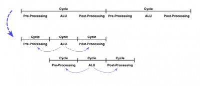
Let's now take a closer look at the pipeline in this design. The objective is to reduce the cycle-time while keeping the cycle-count fixed. The critical path in the CPU falls squarely on the ALU, and associated pre- and post-processing. Rather than cramming all this into one cycle, the basic strategy is to push pre-processing to the prior cycle, and post-processing to the next. This allows the ALU to have the whole cycle to itself, giving us the headroom we need to boost the clock-rate.
Attachment:
 8EE48AA7-1063-4FE1-9FE5-2F36299202AF.jpeg [ 37.24 KiB | Viewed 1240 times ]
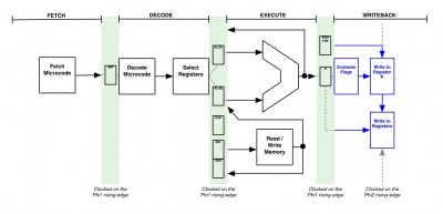
Pre-processing here refers to the work required to set up the inputs to the ALU with appropriate values. That seemingly innocuous task takes a surprising amount of time -- we have to fetch microcode, decode control signals, select source values and output-enable the approriate registers. Post-processing, on the other hand, refers to updating the status flags and writing to the destination register. Rebalancing this workload around the ALU, we end up quite naturally with a four-stage pipeline, as follows:
Attachment:
 0A20172C-7EE4-4D9D-96DE-9DFC021A9BF8.jpeg [ 52.57 KiB | Viewed 1240 times ]
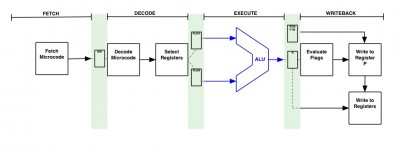
We have FETCH, DECODE, EXECUTE and WRITEBACK -- the idea is to perform a roughly equal amount of work at each stage and then to pass the baton to the next. Along the way, we capture intermediate results in pipeline registers. Specifically, we have the Microinstruction Register (MIR) after the FETCH stage, we have ALUA, ALUB and ALUC registers at the ALU inputs and we have the R register at its output. The FTM (Flags To Modify) and RTM (Registers To Modify) registers direct the WRITEBACK stage regarding which flags and destination register to update. (More on the WRITEBACK stage below.)
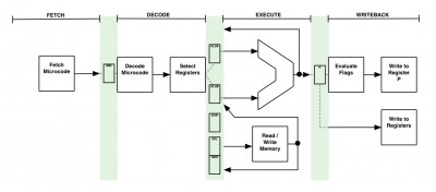
Memory operations using "flow-through" synch RAMs are a good fit for this arrangement. A key feature of these RAMs is that we can clock an address into the RAM's internal registers then read the data value from its outputs before the next clock edge occurs. The ADL and ADH registers allow the pipeline to work in this same way with asynchronous peripherals. For writes, there is also the WE register and a Data Output Register (DOR).
Attachment:
 D50672AF-FBC0-4152-8AC2-424CA09C1F35.jpeg [ 60.45 KiB | Viewed 1240 times ]
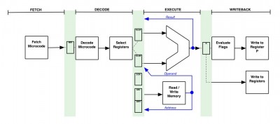
As we've discussed before, the ALU features a "recirculate" path to allow the result to be fed back into its inputs. This is done during address calculation, for example, when the ALU result is immediately required in the next cycle. Memory reads are also recirculated, as either ALU operands or addresses to be used in the next cycle.
Attachment:
 E7B259A6-3F7B-478E-B5C7-D5FBF8A343C2.jpeg [ 64.17 KiB | Viewed 1240 times ]
The WRITEBACK stage calculates the flags based on the ALU result, updates the P register according to the FTM, and writes the result to a destination register according to the RTM.
Attachment:
 16FC68AD-EC89-4E0D-8C9C-6E79EC7FE30A.jpeg [ 76.01 KiB | Viewed 1240 times ]
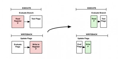
One important thing to highlight is that the WRITEBACK stage writes to registers using a mid-cycle rising clock-edge (PHI2 rising edge). Meanwhile, registers are always sampled at the end of the cycle (PHI1 rising edge). This discipline ensures that we always get an up to date value when a given register is being read and written to in the same cycle. For example, the P register may be updated in the same cycle that a branch test is being executed. Delaying the branch test until the second half of the cycle ensures that the branch test evaluates correctly.
Attachment:
 FE96582E-0EDA-4322-B47B-08E82FCF4BBC.jpeg [ 42.79 KiB | Viewed 1240 times ]
Beyond allowing enough time to calculate the flags, a separate WRITEBACK stage allows the R register to neatly buffer the ALU from the rest of the CPU's internal registers (and the added bus capacitance they would impose). There are over ten destinations for the ALU output, all of which would add unnecessary delay to the ALU's critical path were they connected directly (10 loads x 3pF per load x 50Ω + 6" trace delay = 2.5ns).
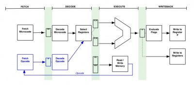
Finally, we should note that the DECODE stage must receive a fresh instruction every cycle in order for the pipeline to function smoothly. To begin with, FETCH retrieves a new opcode from main memory (or simply generates a BRK on a CPU reset) and feeds it to DECODE stage via the Instruction Register (IR).
Attachment:
 7D710D00-CA4C-4635-A91A-B0BB487A09C9.jpeg [ 70.93 KiB | Viewed 1240 times ]
Thereafter, FETCH will retrieve microinstructions associated with that opcode from the microcode store, one per cycle, and feed them to the DECODE stage via the the Mircoinstruction Register (MIR).
Attachment:
 60D1FE67-C0B6-4E71-B174-46F6CF50E679.jpeg [ 68.22 KiB | Viewed 1240 times ]
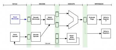
Once we reach the end of the current opcode, a new opcode is fetched and the sequence repeats again. The DECODE stage, meanwhile, always delivers appropriate control signals for downstream pipeline stages, whether by decoding the opcode in one cycle or a microinstruction in another.
And that's it. We'll take a look at how this pipeline executes cycle-accurate 6502 instructions in a future post. For now, the main thing to note is that this is a relatively simple pipeline that still packs a punch in terms of performance. By way of comparison, the critical path on this pipeline is about 20ns long (50MHz) as compared to 50ns (20MHz) on the C74-6502 -- that's assuming similar components in both cases; ie, AC logic for the ALU and CBT logic for tri-state buffers. The hope of course is that faster components and further optimizations (like the FET Switch Adder) will enable us to double the clock-rate yet again and reach the 100MHz milestone. Only time will tell whether we'll manage to get there.
Cheers for now,
Drass
P.S. Many thanks to Dr Jefyll for helping to clarify and edit this description. It is much better for it. Thanks Jeff!


