6502.org Forum  Projects  Code  Documents  Tools  Forum
It is currently Fri Apr 26, 2024 6:07 am

All times are UTC


Post new topic Reply to topic  [ 182 posts ]  Go to page 1, 2, 3, 4, 5 ... 13  Next
Author Message
PostPosted: Tue Sep 08, 2020 11:49 pm 
Offline
User avatar

Joined: Sun Oct 18, 2015 11:02 pm
Posts: 428
Location: Toronto, ON
An often repeated refrain is that homebuilt CPUs are constrained to single-digit clock-rates by limitations inherent in discrete-component design. But we know that's not true. The C74-6502 achieved a 20MHz clock-rate while still being a full-fledged cycle-accurate 6502. It's worth asking, then, could a humble TTL 6502 reach that rarified air above 100MHz? It’s not clear such a thing is possible, but the challenge is on!

We're picking up where we left-off on Ideas for a faster TTL CPU. Team C74 is once again on hand and the objective is to build a next generation TTL 6502 with the highest clock-rate we can muster. The focus will be on reducing the cycle-time while keeping CPI fixed. The over-arching goal as always is to learn and to have fun. This project promises ample opportunity for both, so we'll buckle-up and get ready for a bumpy ride! :)

The effort breaks down into a few key strategies:

1) Use faster hardware
2) Optimize critical circuits
3) Increase parallel processing
4) Manage signal integrity

Let's look briefly at each in turn.

Memory is a key area where faster hardware is essential. Both external memory and the microcode store will need to keep up with a faster clock-rate. Fortunately, access-time can be reduced almost at will using RAM. Hobby-friendly 10ns RAMs are readily available, and synch RAMs are even faster. The latter expect an addresses in advance of the cycle, and deliver in return access-times that are vanishingly small. It's safe to say memory is not likely to be a bottleneck in this design.

By the same token, there are also faster logic families available. The 3.3V LVC family, for example, has a good selection of parts at almost twice the speed of AC logic. The CBTLV family offers 3.3V variants of FET switches which can be very fast when deployed correctly. And then there is the AVC and AUC families. With near-nanosecond propagation delays, these families also feature variable impedance outputs which "provide great signal integrity without the need for external termination when driving traces of moderate length (less than 15 cm)". All-in-all, it's an embarrassment of riches when it comes to fast components.

But there are limitations also. For example, there is no equivalent to the 74AC283 Adder in these faster families, and FET switches are no faster with Select signals than their AC family cousins. Some careful design will be needed in critical circuits to capture the potential gains. Dieter's FET Switch Adder is a good example this, but there are others. The Decode, Flag Evaluation, and Branch Testing circuits are a few examples that are likely to land on the critical path.

Beyond specific optimizations, we'll need to look to increased concurrency. The C74-6502 divided its processing into two stages: the FETCH stage, and the everything-else-stage (aka EXECUTE). An obvious improvement is to split EXECUTE into shorter phases. As we discovered, pipelining can get very complicated very quickly, with multiple caches, hazard checks and branch prediction schemes. So we'll need to be careful lest the whole thing get out of hand. Thankfully, there are significant gains to be had with more TTL-friendly techniques. More on that later.

The final leg of the race is all about signal integrity. Trace geometry, stackup and clock management will all need careful attention. We are likely to need six layers boards, impedance controlled traces and a mixed-voltage supply. It's gonna be fun. (My new bedtime reading is Dr. Johnson's Handbook Of Black Magic)

Alright, so that pretty much lays it out. It's good to be back with Team C74, and we're looking forward to the thrills and spills of this design. But let's take a moment now to pay homage to what is probably the fastest discrete component CPU ever built -- the Fluroinert-cooled Cray 2 supercomputer, clocking in with a 4.1ns cycle in 1985. It's a sight to behold:

Image

I will never forget standing in a darkened observation gallery at Cray Research in the late eighties, and peering into the blueish glow of the demo-lab. Two lab-coated engineers were soberly pulling boards from that now famous circular tower at the center of the room. It was the stuff of legends. The Cray 2’s predecessor, the aptly-named Cray 1, had topped out at 85MHz in 1976, and here was a 244MHz machine. It was not until 1992 that DEC Alpha and HPPA RISC finally took the industry as whole beyond the 100MHz mark.

So is it possible for a discrete-component 6502 to reach that same 100MHz milestone? Well, we're gonna try to find out!

Cheers for now,
Drass

P.S. I wonder how hard Seymour would have worked to try to clip off that last 100ps from the 4.1ns critical path? :)

——————————-
Quick Links

For easy reference, here are some links to posts on specific topics:
  1. Register Clocking
  2. ALU Overview
  3. FET Adder
  4. FET Adder tpd
  5. FET Incrementer tpd
  6. Decimal Mode
  7. Pipeline Description (1)
  8. Flag Evaluation
  9. Pipeline Description (2)
  10. Microcode Description
  11. Critical Path
  12. Logism Model V1
  13. Aspirational Spec
  14. NMOS Quirks and Quarks
  15. Investigating 65816 Support

_________________
C74-6502 Website: https://c74project.com


Last edited by Drass on Sun Dec 27, 2020 6:46 pm, edited 8 times in total.

Top
 Profile  
Reply with quote  
PostPosted: Wed Sep 09, 2020 9:15 pm 
Offline
User avatar

Joined: Sun Oct 18, 2015 11:02 pm
Posts: 428
Location: Toronto, ON
Alright, right up front, we should tackle the ALU, and more specifically the adder. I finally had a chance to test ttlworks' FET Switch Adder. This is an important element of the design and right at the center of the critical path. Within the ALU, the inputs to the adder will be registered, and its outputs will go to the address lines of synch RAM (among other destinations). So the critical path will include the CLK-to-Q delay of the input registers, the Address-to-CLK setup time for the RAM, and a couple of buffers in between. At 100MHz, we get just about 6.5ns available for the adder itself!

The FET Switch Adder uses the fast data-to-Y tpd through the swtiches for the all-important ripple-carry chain. The data inputs are subject to the much slower Sel-to-Y tpd of the switches, but that delay is incurred only once for the whole chain. For the test, I used a variation as suggested by Dr Jefyll, with 74CBTLV3253 muxes, as follows:
Attachment:
sch5.png
sch5.png [ 40.37 KiB | Viewed 7730 times ]

The central challenge in the circuit is the build-up of capacitance along the carry chain. To explore the issue, the test sets up the carry chain to oscillate and trigger a 74LVC163 counter. We can configure the chain as 8-bits or 12-bits, and measure the frequency of oscillation as divided by the counter. The carry chain can also be split with an optional buffer (AND gate) after the 4th element to reduce the capacitance. The whole thing sits on about 1.5 square inches of board space:
Attachment:
626A2BF0-C257-4744-B568-FBE30E8A91A9.jpeg
626A2BF0-C257-4744-B568-FBE30E8A91A9.jpeg [ 44.82 KiB | Viewed 7730 times ]

At these distances, we don't have to worry about transmission line effects, so all connections are unterminated. Here's a trace of the counter output:
Attachment:
FETSwitchAdder3.3V.png
FETSwitchAdder3.3V.png [ 17.47 KiB | Viewed 7730 times ]

We're probing pin 11 on the '163 counter (divide by 16 output), and the carry-chain is configured as two 4-bit segments linked with the AND gate. We can calculate the tpd of the carry-chain based on the 4.29MHz measured frequency as follows:

--> 8-bit carry-chain w/ AND gate: 4.29 MHz x 16 = 68.64 MHz = 14.5ns period / 2 = 7.25ns tpd

Removing the AND gate from the circuit is pretty much a wash -- the delay from the added capatiance is just about equivalent to gate delay we take out:

--> 8-bit carry-chain, no AND gate: 7.2ns

So, we have about 0.9ns per bit. The 12-bit carry chain showed a pretty linear growth in the delay, with 0.9ns per bit as well:

--> 12-bit carry-chain: 10.8ns

So, it turns out that the Elmore Delay calculation I used to estimate the performance of the carry-chain was wildly optimistic. So much for the theory. In practice, the tpd of the adder includes the carry chain plus the switch-time of the 74CBTLV3253, which is 2.9ns (typical). That will remove one bit from the carry chain, so a net addition of about 2ns. The final inverter in the chain should be counted since the carry chain will need to be buffered from the rest of the CPU. So that gives us about 9.2ns for the “A to C” tpd of an 8-bit 74CBTLV3253 FET Switch Adder (roughly 1.2ns per bit).

Not bad at all, and certainly MUCH faster than an equivalent circuit using conventional gates (a conventional ripple-carry adder would be roughly 3ns per bit with NC7SV logic). So a great result, all told, but unfortunately not quite fast enough for 100MHz operation. We’ll have to keep working to squeeze out just a little more performance out of this circuit. :)

Cheers for now,
Drass

_________________
C74-6502 Website: https://c74project.com


Top
 Profile  
Reply with quote  
PostPosted: Sun Sep 13, 2020 10:57 pm 
Offline
User avatar

Joined: Sun Oct 18, 2015 11:02 pm
Posts: 428
Location: Toronto, ON
Here is a different take on the FET Switch Adder. This one relies on a 2:1 74AUC2G53 FET Switch. (Thanks to Dr Jefyll for suggesting this part). This configuration requires an additional gate, but capacitance on the carry-chain is lower — AUC parts have lower intrinsic capacitance to begin with, and the carry chain now connects to one pin on the switch rather than two, as follows:
Attachment:
EvolSch.png
EvolSch.png [ 22.9 KiB | Viewed 7576 times ]

Here is the test circuit:
Attachment:
V2sch.png
V2sch.png [ 96.41 KiB | Viewed 7576 times ]

I took the opportunity to extend the carry chain to better simulate a 16-bit incrementer. This circuit also includes four AND gates in series to simulate carry lookahead feeding the final four bits of the adder. Here is they layout of the test board:
Attachment:
V2brd.png
V2brd.png [ 31.43 KiB | Viewed 7576 times ]

74AUC08 ICs are only available in a VQFN package, so I thought I would experiment with that in passing. Honestly, the footprint (bottom center on the board) looks about the same size as the other VSSOP packages, and the big center pad makes routing harder. Not sure I get the advantages. Anyway, I have added thermal vias to the centre pad as per the datasheet. Not sure these are fully necessary, but I understand they make hand-soldering easier. My instinct for soldering these is to use a hot air gun and reflow pre-tinned pads, rather than fuzzing with solder paste. If anyone has had any experience with QFN please chime in. All suggestions welcome.

Incidentally, the good folks at PCBWay have very kindly offered to support this project with PCB manufacturing. Many thanks to them for that! I used them for all my prior boards, so I’m happy to continue to do so. For now, these little test boards are quite straight forward. I’m sure I will welcome having a contact to talk to when we get to the more demanding impedance controlled boards.

Cheers for now,
Drass

_________________
C74-6502 Website: https://c74project.com


Top
 Profile  
Reply with quote  
PostPosted: Thu Sep 17, 2020 2:02 am 
Offline
User avatar

Joined: Sun Oct 18, 2015 11:02 pm
Posts: 428
Location: Toronto, ON
While we wait for the new test board, let's take a closer look at the ALU. The overall structure is actually fairly straight forward:
Attachment:
ALU Block Diagram.png
ALU Block Diagram.png [ 54.24 KiB | Viewed 7477 times ]

There are registers at the inputs, ALUA, ALUB and ALUC. From there, there are independent paths for the adder and other functions in order to keep capacitance as low as possible for the adder. The shift buffers (SHR and SHL) are placed after the OR function so either the ALUA or ALUB can be shifted by feeding a zero to the other input. Logical operations and shifts are both very fast so there is no issue having them in series. There is a dedicated left-shift buffer rather than using the adder to add a value to itself, as is commonly done. This is so we don't have to connect the A and B inputs of the adder together, which would once again add capacitance.

The R and C registers at the outputs of the ALU capture the ALU result and carry at the end of the cycle. There are paths that bypass these registers to recirculate R and C back into the ALU inputs. Thse are required when two inter-dependent ALU operations follow one after the other immediately. This is the case, for example, when adjusting the high-byte during address calculation.

Control signals going to the ALU are applied only at the outputs in order to select the desired ALU operation output. The control signals can therefore be generated without penalty *during* the cycle while the ALU itself is working. The Flags To Modify (FTM) register is used to capture Write-Enable control signals for each flag that must be updated. The flags are actually updated in the cycle following the ALU operation based on the R and C values. The A7, B6 and B7 hold the indicated bits from the A and B inputs and are used to evaluate the V flag.

The theory of operation for the ALU is that all inputs must be prepared and loaded into registers in the prior cycle. At the clock-edge, the ALU begins working immediately, and the results are captured into output registers at the very end of the cycle. The ALU is thus bracketed by registers on both sides, and can be neatly inserted as a pipeline stage into the datapath.

One thing to note is that the ALU does not invert the B input of the adder for subtract operations. Instead, the B input is inverted in the prior cycle. This manouver reduces the propagation delay through the adder and conveniently shifts the burden to the prior cycle -- which is typically a operand read of the SBC instruction. There is plenty of time to invert the operand on the way in from memory.

And that's a nice segue to the setup for memory:
Attachment:
Memory.png
Memory.png [ 37.46 KiB | Viewed 7477 times ]

In this design, memory too has dedicated registers, namely ADL, ADH, WE and DOR (Data Output Register). Just as with the ALU, these registers are also loaded in the cycle prior to the memory operation. The result of a memory read is clocked into a register also. but rather than using a dedicated register, the data read is placed directly into an appropriate internal register in the CPU (ALUB, ADL, ADH or IR).

This arrangement is very well suited to synch RAMs, which have registered inputs internally. When using synch RAM, ADL, ADH, WE and DOR merely act as shadow registers to the synch RAM's own internal registers. An asynchronous data bus can run at the outputs of ADL and ADH, where traditional RAM, ROM and other peripherals can operate as usual. Of course, very little time will be available for such peripherals in the normal cycle, so it is likely that all aynchronous I/O will be wait-stated (or buffered). More on that later.

Equipped with these registers, both memory and the ALU can be treated as pipeline stages. In both cases, we set up the inputs in one cycle, the operation is completed in the next, and the result is captured in registers at the end of the cycle. The critical path for the pipeline stage includes the CLK-to-Q delay of the input registers and Data-to-CLK setup time of the output registers. If the output is going directly into synch RAM internal registers (when using the ALU to calculate an address, for example), the setup time of the synch RAM must be met.

At 100MHz, only 6.5ns remain available to the ALU after the initial register tpd and before the synch RAM setup time. Hence all the fuzzing about with the FET Switch Adder to reduce the critical path. We'll have to see how those test boards perform once I get them. Fingers crossed on that. :)

Cheers for now,
Drass

_________________
C74-6502 Website: https://c74project.com


Top
 Profile  
Reply with quote  
PostPosted: Thu Sep 17, 2020 7:11 am 
Offline
User avatar

Joined: Fri Nov 09, 2012 5:54 pm
Posts: 1392
Nice going so far.

It's a pity, that 74AUP1G386 (3 input XOR) and 74AUP1G99 (multifunction gate with output enable) are too slow to be useful,
and it looks like no 74AUC version of these chips is in production... yet.

74AUP1G58 is too slow, and there seems to be no 74AUC1G58 in production.
74AUP1G58 can be configurated to work as 2 input AND, 2 input OR, 2 input XOR.
Using only one type of chip for implementing all of the AND\OR\XOR gates would have simplified logistics for ordering parts.
//Since we are at it: in theory, 74AUC1G08 could be substituted by 74AUC2G53, but this won't do good to the capacitances in the carry chain.

There seems to be no "74F298\74F398 equivalent" in 74AUC (2:1 multiplexer plus latch in one chip).
This could have have made it possible to go for a more compact ALU output section.


I'm afraid that inverting B in front of the ALU input latches for having A-B might have a habit of increasing complexity of the control circuitry.
Also, when inverting the data from main memory with XOR gates on their way into the ALU input latches,
I think at 100MHz+ we need to be a little bit more paranoid about the capacitances piling up at the CPU external bus system.


Top
 Profile  
Reply with quote  
PostPosted: Thu Sep 17, 2020 8:03 am 
Offline
User avatar

Joined: Fri Nov 09, 2012 5:54 pm
Posts: 1392
Considering that you would have to calculate "Direct_Register + X\Y + Offset" for some of the 65816 addressing modes,
it might be worth a thought on giving the ALU a three input adder, but this won't do good to the propagation delays.
Google patents: US4783757A.

//80386 had a 3 input adder in the "Segmentation Unit".


Another option would be having shadow registers containing "Direct_Register + X\Y", but I think this would increase complexity of the design,
because then you would need to keep track of changes in "Direct_Register and X\Y".


Top
 Profile  
Reply with quote  
PostPosted: Thu Sep 17, 2020 12:41 pm 
Offline
User avatar

Joined: Fri Nov 09, 2012 5:54 pm
Posts: 1392
Another thought:
In our 20 MHz TTL CPU, we had only one ALU which did arithmetic and logic.
We had used 4:1 multiplexers for implementing the logic units.

Your new block diagram shows separate blocks for arithmetic and logic.
//BTW: how would you increment/decrement memory or X\Y with that design, I think this isn't mentioned in your text above in this thread.

Fact is, that the AND and XOR logic function already is covered by the AND and XOR gates inside the adder (input section).
But tapping into these gates (plus an array of OR gates) with FET switch multiplexers doesn't look like quite the thing.

I guess you are out to put XOR gates in front of the inputs of the ALUB latches for implementing A-B.
If we would have fast 4:1 multiplexers, we could put them as logic units in front of the inputs of the ALUB latches instead,
but even FET switch adders have a considerable propagation delay from select inputs to outputs,
so this also doesn't look like quite the thing.


In theory, one could break the ALU into two parts:
ALUA\ALUB_latches > logic_units > propagate\generate_latches > carry_chain > ALU_output_latches (including shift right),
this buys the carry chain and main memory some more time "to do the job",
but a longer pipeline for data calculations (plus maybe a separate adder for address calculations) won't simplify the design.

Decisions, decisions.


Top
 Profile  
Reply with quote  
PostPosted: Fri Sep 18, 2020 5:27 am 
Offline
User avatar

Joined: Fri Nov 09, 2012 5:54 pm
Posts: 1392
Cray 2 uses 16-gate array logic chips.
It's an interesting question whether a CPU built from gate arrays counts as "discrete CPU" or not...
...and where to draw the line, for instance: Fujitsu\Siemens 7880 and Siemens ECL gate arrays (chips with 64 pins and up to 700 gates).

;---

Some years ago, I had seen a PCB from a CDC Cyber 995.
//There isn't much info about the Cyber 995 (ca. 1987 ?) in the internet.

Don't know what was the function\purpose of that PCB in the computer.
Can't remember much of the details, but I had spotted some MC10181 or MC100181 ALU chips on that PCB.

Cyber 995 had "a 8ns clock", so you better make it a 125MHz+ 6502 for breaking the speed world record. :)

Hmm... chances of making your CPU cycle compatible to a 6502 would decrease exponentially with increasing pipeline depth.
Another interesting question is if whether you still would be supporting decimal mode (and how) or not.


Last edited by ttlworks on Fri Sep 18, 2020 10:34 am, edited 1 time in total.

Top
 Profile  
Reply with quote  
PostPosted: Fri Sep 18, 2020 10:30 am 
Offline
User avatar

Joined: Thu Apr 11, 2019 7:22 am
Posts: 40
Wow, this is all very interesting and a great leaning opportunity for those (like me) who are not used to hardware design. I can't really contribute with anything at this level, but I have a question about the ALU dedicated Shift Left implementation. Allegedly, this is done "so we don't have to connect the A and B inputs of the adder together, which would once again add capacitance." I understand this is the case because this ALU has an independent path for the adder. Now, I suppose this is a bit off-topic but, does this also affect the original implementation featuring logic unit multiplexers before the adder, as per the Dieter docs?


Top
 Profile  
Reply with quote  
PostPosted: Fri Sep 18, 2020 11:24 am 
Offline
User avatar

Joined: Fri Nov 09, 2012 5:54 pm
Posts: 1392
There are different approaches for shifting left, and they all have their pros and cons.
Now to name three approaches: (don't worry, I'll stick with old "Dieter docs" from 2012)

;===

0) In our old 20MHz TTL CPU, the ALU was built from multiplexers working as LUs (logic units) feeding the inputs of a 74283 based adder.

Image

When routing A to both inputs of the adder, we have Q=A+A, that's identical to Q=2*A or Q=SHL(A).
Same thing for B.

Unfortunately, 74283 chips would be way too slow for being useful at 100MHz,
so the ALU for a 100MHz+ CPU has to be built in a different way, avoiding the use of 74283 four Bit adder chips.

;---

1) Now, if we take a closer look into the innards of a binary full adder,
we see A and B feeding a half adder:

Image

//Processing the carry from a lower Bit requires an additional half adder per Bit, but I'm getting off topic.

When replacing these two logic gates at the inputs of a binary full adder with multiplexer based LUs (logic units),
our adder mutates into an ALU like this:

Image

When the P (propagate carry) LU emits 0, and when the G (generate carry) emits A, the ALU shifts A left.
Same thing for B.

;---

2) Another approach is shifting the 8 Bit ALU output left by running it through eight 2:1 multiplexers.

It simplifies the PCB layout when using two 74245 buffers instead of eight 2:1 multiplexers.

First 74245 does not shift:
Q7,Q6,Q5,Q4,Q3,Q2,Q1,Q0 > D7,D6,D5,D4,D3,D2,D1,D0.

Second 74245 does shift left:
Q6,Q5,Q4,Q3,Q2,Q1,Q0,GND > D7,D6,D5,D4,D3,D2,D1,D0.

//Shifting right could be done with a third 74245:
//GND,Q7,Q6,Q5,Q4,Q3,Q2,Q1 > D7,D6,D5,D4,D3,D2,D1,D0.

;===

Hope, this helps.
At the moment, I think there are no concrete plans about what the ALU really should look like in the "end product",
and I think we only are collecting some odd ideas now (and to sort them out later).


Top
 Profile  
Reply with quote  
PostPosted: Fri Sep 18, 2020 4:04 pm 
Offline
User avatar

Joined: Sun Oct 18, 2015 11:02 pm
Posts: 428
Location: Toronto, ON
Great comments Dieter, and hello Joan. Nice to see you posting here. Some responses below:

ttlworks wrote:
I'm afraid that inverting B in front of the ALU input latches for having A-B might have a habit of increasing complexity of the control circuitry.
Yes, but not unreasonably so. The control logic needs to know whether we are fetching an operand on behalf of an SBC or CMP or otherwise. It can then enable the inverter as needed for the memory read. So this comes down to, once again, that pesky FetchOperand cycle. You'll recall that it gave us some trouble in the C74-6502 (for single-byte opcodes for example), and it promises to do so again here. More on that later!

Quote:
Also, when inverting the data from main memory with XOR gates on their way into the ALU input latches,
I think at 100MHz+ we need to be a little bit more paranoid about the capacitances piling up at the CPU external bus system.
I agree. Capacitance is the enemy. My current thought it to divide the data bus into two -- a fast, low-capacitance, synchronous bus for RAM, and a slower asynchronous bus that is wait-stated for ROM and I/O. We can afford to be a little more complacent on the asynch bus.

Quote:
Considering that you would have to calculate "Direct_Register + X\Y + Offset" for some of the 65816 addressing modes,
it might be worth a thought on giving the ALU a three input adder, but this won't do good to the propagation delays.
Google patents: US4783757A.
Very interesting! I considered a three-input adder for a cycle-accurate 65816 implementation. But I was thinking more of hybrid configuration, combining a full 8-bit adder and with a high-byte increment circuit. It would be a little faster than a 16-bit adder since the high-byte propagation would be reduced, and it would eliminate the need for an additional cycle to adjust the high-byte of addresses (or the bank-byte as the case may be). It would also allow 16-bit registers to be incremented and decremented in a single cycle. It may still be possible to do that if the FET Switch Adder is fast enough! :)

Quote:
I guess you are out to put XOR gates in front of the inputs of the ALUB latches for implementing A-B.
Yup, that’s the plan.

Quote:
If we would have fast 4:1 multiplexers, we could put them as logic units in front of the inputs of the ALUB latches instead,
Ha, that’s cool. Pushing ALU logic upstream. But heck, let's extend it further and put an LU right into the memory unit itself! Not something for this design, but what if we implemented "smart" memory that can operate on data without bringing it into the CPU at all. A dual-port RAM where you give the memory unit source addresses, a destination address and an operator, and it performs the operation by itself in the next cycle. Meanwhile, the CPU could be doing something else!

Quote:
8ns machine cycle, so you better make it a 125MHz+ 6502 for breaking the speed world record. :)
At these speeds, 2ns is a mountain! We might have to be satisfied with matching HPPA and DEC Alpha at 100MHz. :)

Quote:
Hmm... chances of making your CPU cycle compatible to a 6502 would decrease exponentially with increasing pipeline depth.
Yes. The current design is still cycle-accurate, but going further would start to add cycles. We need to hit a sweet-spot here. Otherwise, we get shorter cycles, but more of them!

Quote:
Another interesting question is if whether you still would be supporting decimal mode (and how) or not.
Yes, with an additional cycle like in the 65C02. It would not be a pipeline stage, but rather just a wait-state. I think it's a reasonable compromise for Decimal Mode. It happens rather infrequently in the instruction stream, and there is signficant hardware overhead in making the BCD-adjust curcuit a distinct pipleine stage. It would require hazard-checking logic on the A register, which I would rather avoid to keep the pipeline TTL-friendly. :)

joanlluch wrote:
does this also affect the original implementation featuring logic unit multiplexers before the adder, as per the Dieter docs?
Deiter’s original LU design does not connect the A and B inputs together per se. The LUs themselves are used to duplicate the A or B inputs as necessary for the adder which is in series. In this design, the A and B inputs would have to be explicitly connected together in order to use the adder for a left shift. It’s hard to know whether the additional capacitance is worth worrying about in fact. We will know better once the FET Switch Adder tests are complete.

_________________
C74-6502 Website: https://c74project.com


Top
 Profile  
Reply with quote  
PostPosted: Sat Sep 19, 2020 4:52 pm 
Offline
User avatar

Joined: Fri Dec 11, 2009 3:50 pm
Posts: 3346
Location: Ontario, Canada
Drass wrote:
Here is a different take on the FET Switch Adder. This one relies on a 2:1 74AUC2G53 FET Switch.
Attachment:
EvolSch annotated.png
EvolSch annotated.png [ 30.45 KiB | Viewed 7261 times ]

Hello, all. Re the FET Switch Adder, here are a few suggestion/observations, the first admittedly perhaps more fuss than it's worth. As Drass noted, it's important to minimize loading (capacitance) on the carry chain. To that end, it might make sense to insert a series resistor as shown above in a few of the less-significant bit slices (where the resultant delay increase in that bit's SUM output can be afforded). To some extent the resistor would isolate the chain from the XOR gate's input capacitance, and that would sharpen the rise time at that node and thus speed up the chain overall. The improvement would be diluted somewhat because the resistor itself has a certain capacitance to ground; I don't know how much. But even a small net speed increase would make this idea worthwhile.

A more clear cut issue relates to the drive capability of the device(s) driving the carry chain... and of course stronger drive capability means less delay overall. In the unmodified example (left side of the image), each slice drives its C_Out by connecting it to either Vcc or to C_Out from the preceding slice. This means the chain's worst-case drive capability is dependent on a single device -- ie, the flipflop (or whatever) that drives C_In of the least-significant slice. The drive capability of that device is something we would consider carefully.

By contrast, in the modified example on the right the drive for each slice is taken either from the preceding slice or from that individual slice's AND gate, meaning that the worst-case drive capability is now dependent on the individual AND gates near the beginning of the chain. AUC series devices may possibly not be the best choice; something stronger (even though a little slower) might turn out to make more sense. (Or maybe the extra drive should come from two AUC AND gates wired in parallel!)

Finally, the effective speed of the chain is limited by what's deemed to be an acceptable signal level at the final C_Out. We can't afford to wait until this node's voltage approaches one rail or the other; instead, we need to resolve a 49- or 51%-ish voltage into 1 or 0 as soon as can reliably be done. The test board appropriately includes a Schmitt trigger, but if its hysteresis could be reduced then that might aid our cause.

-- Jeff

_________________
In 1988 my 65C02 got six new registers and 44 new full-speed instructions!
https://laughtonelectronics.com/Arcana/ ... mmary.html


Top
 Profile  
Reply with quote  
PostPosted: Mon Sep 21, 2020 1:50 pm 
Offline
User avatar

Joined: Fri Nov 09, 2012 5:54 pm
Posts: 1392
Surprised me to see AM29C334 and ADSP3128 register files from Rochester Electronics at DigiKey
(although at a price that raises an eyebrow), but these chips are too slow for our project anyway.

Edit:
SN74ACT8832 $470. AM29C331 $193, AM29C332 $563.
Very impressive, but again these chips are too slow for our project.

;---

Oh my god:
DigiKey has the MC10H181L 4 Bit ECL ALU for $5.20 //Rochester Electronics
Motorola MECL 1996, PDF page 117.
Propagation delay Cn to Cn+4 2.2ns max.

MC10H179L lookahead carry generator, $1.85

MC10H158 quad 4:1 MUX, $1.85
MC10H173FN quad 2:1 MUX with latch, $1.04

MC10H124, MC10H125, MC10H600..MC10H607: yes, DigiKey has TTL\ECL and ECL\TTL level translators.

MC10H145, 16*4 register file (the ECL equivalent to 74670), 6ns max., $2.85
CY10E474-5KCQ 1k*4 SRAM 5ns, $21.87

Hmm... but no ECL PALs at DigiKey (like National Semiconductor PLDs 1990 PDF page 308: PAL1016RM4A).
No ECL PROMs at DigiKey (like Fairchild 10416).

It's a pity, that 10K and 100K ECL are not compatible:
100179 carry lookahead generator, $4.63
100181 BCD ALU, $8.19

//List is from September 2020.

;---

Edit: The interesting question here is, whether Rochester Electronics only has old Motorola wafers stored in nitrogen, or really might be able to manufacture ECL silicon.
Edit 2: "RoHS non-compliant", I interpret this as "old Motorola chips, not wafers".

If there is a limit to the amount of ECL chips available, there is a limit to the amount of CPUs that could be built when resorting to ECL chips.


Last edited by ttlworks on Mon Oct 05, 2020 5:53 am, edited 1 time in total.

Top
 Profile  
Reply with quote  
PostPosted: Thu Sep 24, 2020 5:46 am 
Offline
User avatar

Joined: Fri Nov 09, 2012 5:54 pm
Posts: 1392
Considering that HP 8082A Pulse Generator repair, I had spent some thoughts on transistorized ECL.

Building something like a ECL 6502 (not 65C02) from transistors doesn't look feasable for some reasons:
0) at 100MHz+, ECL to TTL voltage level conversion isn't trivial. //Anybody who knows PNP switching transistors 2ns or faster ?
1) considering Hanson's block diagram, the CPU won't be small, and routing/distributing the many control signals would kill some of the speed.
2) a CPU of that size probably would burn more than 40W.

Edit:
Fairchild FACT Data Book 1987, PDF page 53, something about TTL\ECL and ECL\TTL logic level conversion.
Unfortunately NECL, not PECL.

Cute, now back to 74AUC\74AUCH.


Last edited by ttlworks on Fri Sep 25, 2020 5:40 am, edited 1 time in total.

Top
 Profile  
Reply with quote  
PostPosted: Thu Sep 24, 2020 8:05 pm 
Offline
User avatar

Joined: Sun Oct 18, 2015 11:02 pm
Posts: 428
Location: Toronto, ON
The boards are here! I’m excited to see how the new FET Adder performs. With some luck, I’ll get a chance to test things this weekend.

In the meantime, here’s an issue to dig into — clock-skew. The cycle is so short in this design that even small delays on clock signals will be material. For example, clock signals that arrive at registers late can encroach into the following cycle and consume valuable time. At the same time, purposeful delays on mid-cycle clock signals can be useful to manipulate the duty cycle (allowing long and short legs of combinatorial logic to share the cycle more equitably, for example). Either way, gaining control over clock line delays is going to be important.

What kinds of delays could we be dealing with? Suppose we have a clock signal internal to the CPU with a 1.2ns rise-time (Tr) driving a 5" trace with ten flip-flops on it. A 50Ω trace on FR4 will present 3.3pF of parasitic capacitance per inch, and each flip-flop will add 3pF of capacitance in addition (assuming AUC logic). The cumulative delay on that trace is something in the order of 3.5ns relative to the input clock signal (i.e., prop delay = Tr + RC, so 1200ps + (5 * 3.3pF * 50Ω) + (10 * 3pF * 50Ω) = 3.5ns). 3.5ns may not seem like much, but it represents more than a third of the cycle at 100MHz!

The moral of the story is to manage capacitance on clock lines carefully. To that end, I'm contemplating using a CDCVF310 1:10 Clock Driver to distribute the clock around the board. A two level clock tree can provide a dedicated trace for up to 100 destinations with minimum capacitance. We can then adjust for the tpd of the clock drivers themselves by using a CY2302 Zero-Delay-Buffer (ZDB) to synchronize these internal signals to the input clock.

Beyond capacitance, there are four key specs in the CDCVF310 clock-driver datasheet that we should examine to better understand skew:

Tpd = 2.8ns max -- Propagation Delay: CLK input to Yn output propagation delay
Tsk(o) = 150ps max -- Output Skew: the variation in the tpd between outputs, i.e., from Ym to Yn
Tsk(p) = 250ps max -- Pulse skew: the variation in tpd from PLH to PHL
Tsk(pp) = 350ps max -- Part to Part skew: the variations in tpd from various ICs on the board

With a multi-level tree, all four specs may come into play, and the total skew can add up to be a problem if we're not careful. Consider two Flip-Flops in series, like this:
Attachment:
CLKFF.png
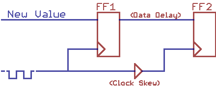
CLKFF.png [ 2.26 KiB | Viewed 7059 times ]

If the clock-delay from FF1 to FF2 is longer than the tpd of FF1 plus the data delay to FF2, then FF2 will not latch the intended value correctly and the circuit will fail. One way to ameliorate the problem is to use trace delays in our favour. We can wire CLK signals so traces go from downstream flip-flops to upstream ones, hence clocking them in reverse order. Another option is to introduce delay in the data signals until the travel time between the flip-flops exceeds the longest clock-skew by some safety margin.

And that brings us neatly into the issue of Write-Enable signals (WE) and how they might impact skew. We have a few implementation options to consider:

1) On the C74-6502, write signals are all routed to a 74AC273 register and released together on the clock-edge -- like this:
Attachment:
CLK273.png
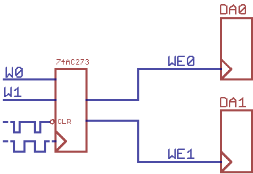
CLK273.png [ 2.52 KiB | Viewed 7059 times ]

The 74AC273 is cleared mid-cycle by a low-going pulse. Active-high WE signals arrive at the 74AC273 at various times throughout the cycle, but then travel to their destinations more or less together. A challenge with using this approach in this design is the potential skew between the outputs of the’273 register. There is no spec for skew mentioned on the 74AC273 datasheet, but it can be as much as 1ns on a 74LVC273. (From the datasheet, Tsk(o) = 1ns max, “Skew between any two outputs of the same package switching in the same direction."). In addition, it’s also more difficut to generate the mid-cycle pulse to clear the ‘273 reliably at these clock-rates.

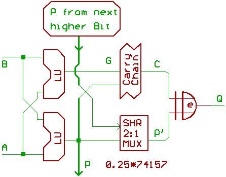
2) To minimize skew, we ideally want nothing in the path between the clock and a flip-flop’s CLK input, as in this alternative based on a 2:1 FET Mux at the data inputs of a register:
Attachment:
CLKMUX.png
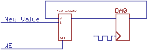
CLKMUX.png [ 1.93 KiB | Viewed 7059 times ]

This method accomodates both active-high and active-low WE signals equally well. The FET switch will add 5Ω of series resistance at the data inputs of the flip-flop, and with it some minimal additional delay that we can safely ignore here. The switch-time of the mux becomes the setup time for the WE signal. One consideration is that clocking all flip-flops every cycle will consume some additional power, but the main drawback is the number of additional ICs required implement the approach. We effectively need one ‘3257 2:1 mux for every 4-bits of registered data in the CPU. That's a lot of hardware overhead.

3) Another approach is to use active-high WE signals with AND gates at the CLK inputs of flip-flops. This gating mechanism is sensitive to glitches if the WE signal is allowed to fluctuate while the clock is high. This is very likely to happen with WE signals that are generated by combinatorial logic. In that case, we can use a transparent latch to hold WE steady during the first half of the cycle, like this:
Attachment:
CLKAND.png
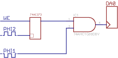
CLKAND.png [ 2.65 KiB | Viewed 7059 times ]

In this case, the datasheet for 74AUC08 lacks any skew information so it’s hard to know what kinds of delay we might be dealing with. We can use the ZDB to synch up the signals with an external clock, but that of course won’t help skew.

4) We can also use OR gates with active-low WE signals, as follows:
Attachment:
CLKOR.png
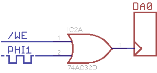
CLKOR.png [ 1.91 KiB | Viewed 7059 times ]

In this case, fluctuations in /WE during the clock-high phase are not harmful. The catch is that once /WE is brought low, the signal must rise again before the following mid-cycle, or a phantom clock-edge will be generated at the flip-flop input when it does rise. The approach is therefore not feasible in situations where WE signals are only available late in the cycle (which is very much the case in this design).

5) Finally, we can use FET switches to gate clock signals, like this:
Attachment:
CLK2G53.png
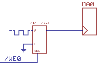
CLK2G53.png [ 1.72 KiB | Viewed 7059 times ]

With this approach, brief fluctuations on the WE signal should not cause a problem. However, longer pulses, or indeed a full switching of the WE signal before the mid-cycle is problematic. Like with AND-gated clock above, a transparent latch could be used to hold WE steady during the first half of the cycle. The advantage here is that the tpd of FET switches is much shorter, and so any deviation from the mean is likely to also be minimal.

I don't doubt there are other approaches to these issues, so please feel free to suggest any alternatives. As always, all input is very much welcome. We'll have to see how all this works out in the final analysis. For now it's safe to say that clock-skew, trace-delay and write-enable signals will all need to be carefully managed if we are to get anywhere near the 100MHz goal.

Cheers for now,
Drass

_________________
C74-6502 Website: https://c74project.com


Top
 Profile  
Reply with quote  
Display posts from previous:  Sort by  
Post new topic Reply to topic  [ 182 posts ]  Go to page 1, 2, 3, 4, 5 ... 13  Next

All times are UTC


Who is online

Users browsing this forum: No registered users and 33 guests


You cannot post new topics in this forum
You cannot reply to topics in this forum
You cannot edit your posts in this forum
You cannot delete your posts in this forum
You cannot post attachments in this forum

Search for:
Jump to: