6502.org Forum  Projects  Code  Documents  Tools  Forum
It is currently Tue May 07, 2024 10:29 am

All times are UTC


Post new topic Reply to topic  [ 4 posts ] 
Author Message
PostPosted: Fri Mar 05, 2021 4:31 pm 
Offline
User avatar

Joined: Wed Aug 17, 2005 12:07 am
Posts: 1207
Location: Soddy-Daisy, TN USA
I am getting really close to laying out my next PCB.

One of the mistakes I made in my last PCB was my through-hole resistor footprint sizes. They were so short that I had to stand the resistors up vertically! I don't know how I made that mistake. LOL

So what I thought I would do is find some other boards around my house and measure the resistor sizes, cap sizes, etc. to see what they used.

But I'd also like to ask your opinions. All of my components are through-hole. I'd like footprints to be as small as possible but still large enough to work with.

Any tips would be appreciated on sizes. I didn't see anything like that in the primer or tips of the day.

Thanks!

**EDIT**

For the resistor, I'm thinking maybe using L11.9mm, D4.5mm, P20.32mm. Does that look about right?


Attachments:
Resistor.PNG
Resistor.PNG [ 42.15 KiB | Viewed 927 times ]

_________________
Cat; the other white meat.
Top
 Profile  
Reply with quote  
PostPosted: Fri Mar 05, 2021 4:57 pm 
Offline
User avatar

Joined: Thu May 28, 2009 9:46 pm
Posts: 8176
Location: Midwestern USA
cbmeeks wrote:
But I'd also like to ask your opinions. All of my components are through-hole. I'd like footprints to be as small as possible but still large enough to work with.

Leaded capacitors and resistors are produced in standardized physical sizes for a given rating. In a computer circuit, the most numerous capacitors are the bypass units associated with the different chips. The usual capacitor type is an MLCC rated at 0.1µF/50 volt, which in radial-lead packages can be had with 0.1" lead spacing. They are available in 0.2" and 0.3" as well, which sometimes is more convenient. However, smaller lead spacing means shorter leads and less lead inductance.

Bypass capacitors with 0.1" lead spacing are quite small and with a little bit of imagination, can often be buried inside the open space in a chip socket. Another construction method is to mount them on the solder side of the board.

Regarding resistors, a common axial-lead size in logic circuits is 1/4 watt, which easily mounts in a hole spacing of 0.35". If you have a number of resistors of the same value and they are physically close to each other, a resistor SIP can save quite a bit of space and sometimes even help with trace routing. SIPs typically have a 0.1" pin spacing and are made in bused and isolated styles. The former is like several resistors with one lead of each connected to a common point. Isolated is several resistors with each one's leads individually brought out.

If you use a SIP pay attention to both the individual resistor wattage rating and the rating for the entire package. Oftentimes, the package rating is less than the sum of the individual resistors' ratings. In most logic circuits that rating limitation shouldn't be a problem.

_________________
x86?  We ain't got no x86.  We don't NEED no stinking x86!


Top
 Profile  
Reply with quote  
PostPosted: Fri Mar 05, 2021 5:05 pm 
Offline
User avatar

Joined: Thu May 28, 2009 9:46 pm
Posts: 8176
Location: Midwestern USA
cbmeeks wrote:
For the resistor, I'm thinking maybe using L11.9mm, D4.5mm, P20.32mm. Does that look about right?

The body length of a 1/4 resistor is around 0.22" and the diameter around 0.1". Parts sizes of resistors were standardized in decimal decades ago.

As I said above, hole spacing of 0.35" is comfortable—you really don't want to go tighter, as it will mean bending the leads right at the body, which is to be avoided.

_________________
x86?  We ain't got no x86.  We don't NEED no stinking x86!


Top
 Profile  
Reply with quote  
PostPosted: Fri Mar 05, 2021 9:40 pm 
Offline
User avatar

Joined: Fri Aug 30, 2002 1:09 am
Posts: 8432
Location: Southern California
In our company, I've always been pressed for maximum density. When we were doing stuff in thru-hole, I always made it so you almost can't see the board on the component side, because there's no space between components. You might not have any reason to go so dense; but if you want to, you can go a lot smaller than you're showing.

¼W resistors are less than .100" wide, and leaving .100" will be plenty. The label, "R21" for example, goes under the component, not beside it, as you mainly only need it when you're stuffing the board. If you want the reference designator for troubleshooting later, well, you have it on your CAD to look up on the screen. You could put the holes for a ¼W resistor as little as .300" apart (on centers); but for our production people, I always gave it .400". Hole size was .030", and pad size was .050". However, I only used ¼W in the rare case that a 1/8W resistor couldn't handle the power dissipation.

For 1/8W or 1/6W resistors, I put the hole spacing at .250", hole diameter .025", and pad width at .045". Leaving .075" width will always be enough; but if you stagger them like in the pictures below, you can go a lot closer. The two pictures are the same part of the same board (which was nearly all analog, not digital), showing how I put 11 resistors and diodes underneath each 14- or 16-pin DIP, staggered in five rows. The first pictures shows it before one of the ICs (in the top-left corner) was put over them, then the next picture shows it after the IC is installed over them.

Attachment:
denseNoU5.jpg
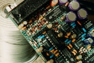
denseNoU5.jpg [ 80.31 KiB | Viewed 902 times ]

Attachment:
denseWithU5.jpg
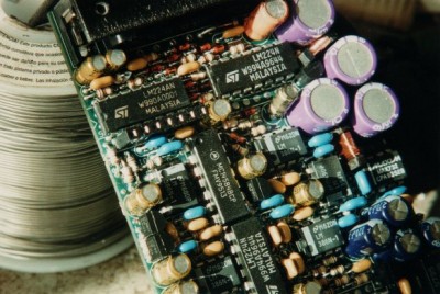
denseWithU5.jpg [ 80.18 KiB | Viewed 902 times ]

(These are shown 2/3 of the way down the "Custom PCBs" page of the 6502 primer.)

The multilayer ceramic capacitors are sometimes available in .1" lead spacing, but I couldn't count on it, at least not back when we were doing this stuff; so I always went for .2" lead spacing. (Then we'd order .2" LS cap.s and what would come be .1's with the leads formed to fit into .2" spots! Grrrr.) The space I left for them was shaped like the racetrack around a football field, .270" long and .100" wide. The holes were .030" diameter and their pads were .050". We never had any production problems with these.

Here's the sandwich the above board went into. The whole thing went into a case hardly bigger than a bar of soap, and had about 500 components in it if it was ordered with all the options. (Actually the one shown is missing a board.)
Attachment:
244eSandwich.jpg
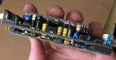
244eSandwich.jpg [ 60.71 KiB | Viewed 902 times ]

Notice that with the mother board and the modules that plug into it on the top, the tall parts miss each other.

_________________
http://WilsonMinesCo.com/ lots of 6502 resources
The "second front page" is http://wilsonminesco.com/links.html .
What's an additional VIA among friends, anyhow?


Top
 Profile  
Reply with quote  
Display posts from previous:  Sort by  
Post new topic Reply to topic  [ 4 posts ] 

All times are UTC


Who is online

Users browsing this forum: No registered users and 6 guests


You cannot post new topics in this forum
You cannot reply to topics in this forum
You cannot edit your posts in this forum
You cannot delete your posts in this forum
You cannot post attachments in this forum

Search for:
Jump to: