6502.org Forum  Projects  Code  Documents  Tools  Forum
It is currently Tue Apr 23, 2024 7:00 pm

All times are UTC


Post new topic Reply to topic  [ 149 posts ]  Go to page Previous  1, 2, 3, 4, 5, 6 ... 10  Next
Author Message
PostPosted: Fri Apr 26, 2019 3:51 pm 
Offline
User avatar

Joined: Fri Nov 09, 2012 5:54 pm
Posts: 1392
Aha. Ralf: What tools you had used for stripping the insulation from Teflon wire ?

RalfK wrote:
My first contact to PCs was to a PET 2000.

Elektor Junior computer hobby kit, later CBM 3016 at school, eventually a C64 at home.

Say... if there would be too many rainy days somewhere in the future,
would you be interested to test if a C74 CPU runs with an Apple, or to build a TTL UART ? ;)


Top
 Profile  
Reply with quote  
PostPosted: Fri Apr 26, 2019 9:58 pm 
Offline

Joined: Sat Aug 19, 2017 1:42 pm
Posts: 35
Location: near Karlsruhe, West-Germany
ttlworks wrote:
Aha. Ralf: What tools you had used for stripping the insulation from Teflon wire ?

Hm, I try to remember this details "some" years later: I think I used the soldering iron.

ttlworks wrote:
Say... if there would be too many rainy days somewhere in the future,
would you be interested to test if a C74 CPU runs with an Apple, or to build a TTL UART ? ;)

A C74 CPU? Maybe in autumn (october or so). There are some 65(C)02 based machines :-) But there are also some other interests i.e. a solution based on hardware and software for reverse engineering of PALs and GALs.
Not to forget this interesting software project: https://www.applefritter.com/content/ar ... -processor

Ralf


Top
 Profile  
Reply with quote  
PostPosted: Thu May 02, 2019 12:14 am 
Offline

Joined: Sun Oct 14, 2012 7:30 pm
Posts: 107
I looked at doing something similar to what you are proposing, and then I explored the option to use just a fast microcontroller to completely emulate the 6502 itself and that is what I stuck with. It's small, cheap, and works. When running code out of the cache or internally mapped memory I can execute up to 8 instructions in one normal PH2 time (1us). These instructions can be anything from a simple NOP to more complex instructions like LDA ($xx),Y. The great thing is that mapping regions as non-cacheable lets normal peripherals (like a 6522) operate at their normal speed. No having to tweak bus speeds on the fly for peripherals is required.

I am still working on support to be able to switch between 6502 (NMOS) and 65C02 versions. I am also working on similar boards to emulate the Z80 and 6809E CPUs. I made a thread about this here:
viewtopic.php?f=8&t=5562


Top
 Profile  
Reply with quote  
PostPosted: Mon May 06, 2019 4:01 pm 
Offline
User avatar

Joined: Fri Nov 09, 2012 5:54 pm
Posts: 1392
Sorry for the delay.

RalfK wrote:
Not to forget this interesting software project

8231 arithmetic processor for the 6502. Nice.
Any facts on the compatibility between 8231, AM9511 and AM9512 ?

Floating point seems to make M$ Commodore BASIC agonizingly slow, how are things with BASIC on Apples ?

Looking forward to seeing a 68881 or 68882 attached to a 6502... someday...
but info about wat actually happens on the bus between 68008 and 68881\68882 already was hard to get
when these chips were in production.

In theory, one could build a TTL FPU for the 6502, but it would be a lot of work... and a different thread, of course.
We just don't have the _time_ now for spending any thoughts on building something like that.


Top
 Profile  
Reply with quote  
PostPosted: Mon May 06, 2019 4:11 pm 
Offline
User avatar

Joined: Fri Nov 09, 2012 5:54 pm
Posts: 1392
But back on ALU design.

Stumbled over the Onsemi\Fairchild NC7SB3257 2:1 FET bus switch, and to me it looks like a "game changer".
5V capable, 250ps propagation delay through the switch, switch resistance 3 Ohm typ. (Vil) and 6 Ohm typ. (Vih).

Attachment:
alu_switch.png
alu_switch.png [ 89.81 KiB | Viewed 2420 times ]


Left: 1 Bit ALU slice.
Right: ALU slice configurated as an adder.

So if we would be going to use 74AC153 multiplexers as LUs (Logic Units), NC7SB3257 2:1 switches for the carry chain and 74AC86 (or faster XOR gates)
for building our carry skip adder, what would be the min\typ\max propagation delay for the ALU ?


Last edited by ttlworks on Wed Jun 26, 2019 5:54 am, edited 1 time in total.

Top
 Profile  
Reply with quote  
PostPosted: Mon May 06, 2019 7:21 pm 
Offline

Joined: Sat Aug 19, 2017 1:42 pm
Posts: 35
Location: near Karlsruhe, West-Germany
ttlworks wrote:
8231 arithmetic processor for the 6502. Nice.
Any facts on the compatibility between 8231, AM9511 and AM9512 ?

i8231 is compatible to AM9511, software and hardware. We bought the Intel chips because they need less power. The AM9512 is different in software and hardware.

I will mainly use the i8231 for 16bit integer multiplication and division within the UCSD p-Machine. The floating point data representation seems to be different to the p-Machines format. I will see ...

ttlworks wrote:
Looking forward to seeing a 68881 or 68882 attached to a 6502... someday...

http://mirrors.apple2.org.za/Apple%20II ... %20Engine/

ttlworks wrote:
but info about wat actually happens on the bus between 68008 and 68881\68882 already was hard to get
when these chips were in production.

Running the 68881/68882 on a 8bit data bus seems to be horrible. These Motorola FPUs were made as compagnion chips to the 68020 coprocessor interface. They use the caches of the CPU and a 32bit data bus.

Regards
Ralf


Top
 Profile  
Reply with quote  
PostPosted: Tue May 07, 2019 5:35 pm 
Offline
User avatar

Joined: Fri Dec 11, 2009 3:50 pm
Posts: 3346
Location: Ontario, Canada
ttlworks wrote:
Left: 1 Bit ALU slice.
Right: ALU slice configurated as an adder.
Great work, Dieter -- very exciting! I agree this could be a game changer (because the use of FET switches minimizes delay in the all-important carry chain).

I don't quite understand the "LU" blocks in the left diagram of your post. But here (below) is a variation on your adder (from the right diagram). It's not any faster, but the chip count is reduced (just two SMD's -- one 6-pin and one 10-pin).

cheers,
Jeff


Attachments:
ADDER using SP4T FET switch.png
ADDER using SP4T FET switch.png [ 3.08 KiB | Viewed 2750 times ]

_________________
In 1988 my 65C02 got six new registers and 44 new full-speed instructions!
https://laughtonelectronics.com/Arcana/ ... mmary.html
Top
 Profile  
Reply with quote  
PostPosted: Tue May 07, 2019 10:22 pm 
Offline
User avatar

Joined: Sun Oct 18, 2015 11:02 pm
Posts: 428
Location: Toronto, ON
I don’t have much to add to the above, except to say WOW! :shock:

Currently, the ALU 8-bit skip-adder is on the critical path:
Code:
ALUA     74AC574    6.0     CLK to Q for input register
ADDER    74AC283   10.6     Lo-byte Adder
SKIP.ADR 74AC257    4.5     Hi-byte Skip Adder
ADR.OUT  74CBT3245  0.25    ALU output select (and latch)
REG.CLK  74AC574    0       Register setup time
Total               21.35ns
Well, now, it seems that this FET-Switch Adder is going to put the critical path elsewhere. Amazing!

The next longest path is the WriteFlags/BranchTest logic, which sits at 20ns. But it currently includes writing to the P register mid-cycle. It’s possible to bypass the register-write with some additional “flag-select” logic in the branch test. This logic would select flag values coming directly from the ALU for those flags that are being modified in the current cycle (i.e. as a result of an ALU operation in the prior cycle). Any flags not being modified would come from the P register. The Branch decision could then be made in parallel with the P register write, and that saves 6ns. (Is this what you were getting at above Dieter?).

_________________
C74-6502 Website: https://c74project.com


Top
 Profile  
Reply with quote  
PostPosted: Fri May 10, 2019 2:57 pm 
Offline
User avatar

Joined: Fri Nov 09, 2012 5:54 pm
Posts: 1392
I think I should elaborate my idea for a different ALU design more detailed.

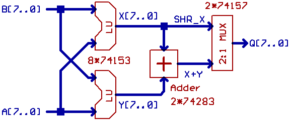
Drass, what we currently have in the CPU are 74153 4:1 multiplexers,
working as logic units, feeding the inputs of 74283 adders:

Image

;...

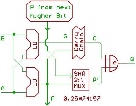
What I'm suggesting is related to the _other_ ALU design described here,
except that the SHR MUX is missing this time.

Image

;---

My suggestion is tossing the 74283 out of the design.

One 74153 contains two 4:1 mutiplexers, which are working as LUs (logic units), emitting the P (propagate) and G (generate) signal for one Bit of data.
(Means, that the ALU control signals for the multiplexers have to be different than they are now.)

The P,G outputs of the two multiplexers per data Bit go to a NC7SB3257 FET switch, 4 FET switches required for 4 Bits of data,
and that's the carry chain.

We need one two input XOR gate per data Bit for generating the ALU output from P and carry, and that's all.

//Maybe tossing the 74283 out of the incrementer\decrementer would make sense, too.

;---

For the two input XOR gate, to me two chips look interesting:
NL17SZ86
NC7SZ86

It's a pity, that there seem to be no XOR gates with three_state output.


Top
 Profile  
Reply with quote  
PostPosted: Fri May 10, 2019 3:03 pm 
Offline
User avatar

Joined: Fri Nov 09, 2012 5:54 pm
Posts: 1392
Ralf, thanks for the link, had not expected to see something like this.

Let's raise the bar: anybody here in the forum who had tinkered with the AM29325 floating point chip ? ;)
And was the heatsink required really as small as in the picture from the data sheet ?


Top
 Profile  
Reply with quote  
PostPosted: Fri May 10, 2019 3:36 pm 
Offline
User avatar

Joined: Fri Dec 11, 2009 3:50 pm
Posts: 3346
Location: Ontario, Canada
ttlworks wrote:
It's a pity, that there seem to be no XOR gates with three_state output.

Dieter, you could consider using 74LVC1G99. It is primarily a 1-bit-wide 2:1 Multiplexer, but its three-state output also has a polarity control. :)


Attachments:
1G99.png
1G99.png [ 1.8 KiB | Viewed 2668 times ]

_________________
In 1988 my 65C02 got six new registers and 44 new full-speed instructions!
https://laughtonelectronics.com/Arcana/ ... mmary.html
Top
 Profile  
Reply with quote  
PostPosted: Fri May 10, 2019 3:51 pm 
Offline
User avatar

Joined: Thu Dec 11, 2008 1:28 pm
Posts: 10793
Location: England
I think you win the prize there for best 74 series gate.


Top
 Profile  
Reply with quote  
PostPosted: Sat May 11, 2019 11:12 am 
Offline
User avatar

Joined: Fri Nov 09, 2012 5:54 pm
Posts: 1392
Jeff, thanks for the hint.
74LVC1G99 also could do the SHR functionality of the ALU.

The problem when building the carry chain from NC7SB3257 FET switches is,
because of the switch resistance and the capacitances in the design to me it's hard to judge what would be faster:
Trying to build an 8 Bit carry chain, or to stick with the carry skip adder topology (4 Bit chunks) we currently have in the TTL CPU.

Would suggest to build a test SBC containing just an ALU and a register for both approaches,
then to configurate the ALUs for "increment" and to see which approach would offer more speed.


Top
 Profile  
Reply with quote  
PostPosted: Sat May 11, 2019 11:19 am 
Offline
User avatar

Joined: Fri Nov 09, 2012 5:54 pm
Posts: 1392
Since the AM29325 was mentioned above, I also took a look at the LVPECL chips.

OnSemi\Fairchild MC100LVEL looks interesting, Microchip\Micrel SY55\SY58 looks interesting, too.

Chips might draw 20..60mA from the power supply, maybe at 5..12€ per chip.
Chips usually contain only one gate, multiplexer or flipflop, and we would be going to need level converter chips too,
so this would take a lot of chips.

IMHO making use of ECL in our CPU _would_ make the CPU a lot faster than memory,
but it will cost too much, draw too much current from the power supply,
and might require something like active (liquid) cooling.

That's like sending the Yamato for sinking a rowboat, in other words: uneconomical.


Top
 Profile  
Reply with quote  
PostPosted: Thu May 23, 2019 3:34 pm 
Offline
User avatar

Joined: Fri Nov 09, 2012 5:54 pm
Posts: 1392
From the datasheet, Microchip\Micrel SY58051 2:1 CML multiplexer is an interesting chip.
If one happens to have all of the signals in inverted and non_inverted form (like when using CML or differential ECL), a 2:1 multiplexer can replace any logic gate.
Edit: at physical layer, it appears that DVI and PCI_express seem to be CML, so it's interesting that there are coventional logic chips in the "CML corner".


Looks like one CML output only can drive one CML input.
But for the other logic families: when building something like a multiplexer or a decoder from something like a tree of 2:1 multiplexers,
the load on the signal lines controlling the multiplexer select inputs usually isn't distributed evenly.

Whygee has written a neat article about creatively stacking 2:1 multiplexers (or SPDT relay switches) in French,
containing some tricks for evenly distributing the load on the control lines.


Top
 Profile  
Reply with quote  
Display posts from previous:  Sort by  
Post new topic Reply to topic  [ 149 posts ]  Go to page Previous  1, 2, 3, 4, 5, 6 ... 10  Next

All times are UTC


Who is online

Users browsing this forum: No registered users and 6 guests


You cannot post new topics in this forum
You cannot reply to topics in this forum
You cannot edit your posts in this forum
You cannot delete your posts in this forum
You cannot post attachments in this forum

Search for:
Jump to: