6502.org Forum  Projects  Code  Documents  Tools  Forum
It is currently Sat Apr 27, 2024 11:58 pm

All times are UTC


Post new topic Reply to topic  [ 149 posts ]  Go to page Previous  1, 2, 3, 4, 5, 6, 7, 8 ... 10  Next
Author Message
PostPosted: Thu Jun 27, 2019 12:48 pm 
Offline
User avatar

Joined: Fri Nov 09, 2012 5:54 pm
Posts: 1392
Looks nice.

To avoid confusion to our readers:
In my hand drawn schematics, ADRLC is C4, and BCDLC is C4'.


Replacing the 74283 BCD.ADJ.LO BCD correction adder (Bit 3..0) by multiplexers and XOR gates would be simple.

Replacing the 74283 BCD.ADJ.HI BCD correction adder (Bit 7..4) by multiplexers and XOR gates would be complicated,
because BCDLC goes into the carry input of that adder.


Unfortunately, feeding the A inputs of the BCD.ADJ.HI adder from the outputs of the SKIP.ADR.BCD.F multiplexer
(instead of the outputs of the ADR.HI.CLO.4..7 adder) for removing BCDLC from the BCD.ADJ.HI adder carry input
(simplifying the BCD.ADJ.HI correction circuitry) would increase the popagation delays a lot.

Need to spend some thoughts on this.
Cheers !


Top
 Profile  
Reply with quote  
PostPosted: Sat Jun 29, 2019 1:14 pm 
Offline
User avatar

Joined: Sun Oct 18, 2015 11:02 pm
Posts: 428
Location: Toronto, ON
[EDIT: Found a useful optimization over the previous circuit ... ]

Here’s where I’m at for the BCD.ADJ.HI adder, which now includes a BCDLC carry input. It’s just the same as the previous BCD.ADJ.LO circuit, but followed by a carry-lookahead incrementer (the carry-look ahead uses a 74LVC138 as a 4-input AND). The XOR gates that followed the MUXes for Q1 and Q2 have been folded into the Multiplexers to make the incrementer more efficient. The combined circuit comes in at 5ns, as follows:
Attachment:
5EF8BBA6-0952-41B0-8B6C-F8D3EA4D9176.jpeg
5EF8BBA6-0952-41B0-8B6C-F8D3EA4D9176.jpeg [ 60.42 KiB | Viewed 2701 times ]

But now I’ve noticed that the [A..F] DETECT.HI ICs are CBT parts, and that means we don’t get /BCDHC for free. An inverter adds 2ns, so in fact this circuit takes 7ns. :evil:

hmmm, a 4-bit FET Switch adder has a higher IC count, but comes in at just 6ns. Gonna have to keep working at this ... :|

_________________
C74-6502 Website: https://c74project.com


Top
 Profile  
Reply with quote  
PostPosted: Sat Jul 13, 2019 5:43 pm 
Offline
User avatar

Joined: Sun Oct 18, 2015 11:02 pm
Posts: 428
Location: Toronto, ON
I’ve been working on refining the critical path for the CPU, and part of that work requires an estimate of the tpd for the new FET Switch Adder.

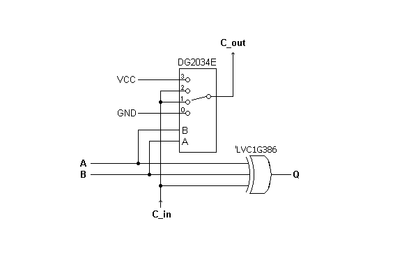
To recall, a 1-bit slice of Dieter’s FET Switch Adder as refined by Dr Jefyll looked like this:
Attachment:
A859E501-88F7-4C86-9213-BEC3D0F19BC4.png
A859E501-88F7-4C86-9213-BEC3D0F19BC4.png [ 3.08 KiB | Viewed 2616 times ]
For our purposes, we can use a 74CBTLV3253 for the 4-way FET Switch. As Jeff suggested, the second channel in the Dual 1-of-4 Mux can be used as a “Logical Unit” (http://6502.org/users/dieter/a2/a2_1.htm) to implement OR, AND and XOR functions for the ALU. All in all, it’s a tidy arrangement.

Ok, the carry-chain in this circuit includes several FET Switches in series, and while the datasheets usually provide a tpd figure for FET Swtiches, they do so with an asterisk:
Quote:
*The propagation delay is the calculated RC time constant of the typical on-state resistance of the switch and the load capacitance, when driven by an ideal voltage source (zero output impedance).
In order to get a better handle on how the likely propagation delays might play out, I set about doing some calculations, which I show below. (I should mention that I am not at all certain about the approach here, and I would appreciate any comments or insights better informed folks might offer).

Alright, moving on ... we have figures from the datasheets as follows:

74CBTLV3253 ON-State Resistance (Ron) — 15Ω
74CBTLV3253 Input capacitance (Ci) — 0.9pF
NC7SV86 XOR Gate Input Capacitance (Ci) — 2pF
IC Following the carry-chain Input capacitance (Ci) — 3pF

The tpd of the final FET Switch in the carry chain is easy to calculate as a simple RC delay. The load is the input capacitance of the IC following the carry-chain (assume 3pF) multiplied by the ON-State resistance of the switch (15Ω) = 45ps (as expected, lightning fast!). The other FET Switches, on the other hand, are not so straight forward to figure out. Googling around a bit, it became clear that the delays here are no longer a simple RC delays. Rather, a better approximation can be calculated as an Elmore Delay (https://en.m.wikipedia.org/wiki/Elmore_delay).

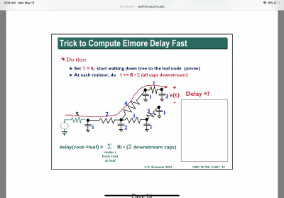
From what I understand, Elmore delays can be used to approximate the delay through an tree-structured RC-Network. Here is a nice illustration of the process:
Attachment:
41568F9C-AB66-4CF6-9907-6F43F2B07715.png
41568F9C-AB66-4CF6-9907-6F43F2B07715.png [ 315.39 KiB | Viewed 2616 times ]
In essence, the delay of each node in the tree is the resistance at that node multiplied by the sum of all downstream capacitance. The total delay through a given network path is the sum of all such RC delays in the path.

In our case, the second to last FET Switch has the following load on it: an XOR Gate pin (2pF) + 2x ‘3253 pins (0.9pF) + the “following IC” pin (3pF) = 6.8pF. So the simple RC delay for this node is 15Ω * 6.8pF = 102ps. Given this, I tallied up the simple RC delays for each of the FET Switches in an 8-bit carry-chain, as follows:

Bit 7 — 0.045 ns
Bit 6 — 0.102 ns
Bit 5 — 0.159 ns
Bit 4 — 0.216 ns
Bit 3 — 0.273 ns
Bit 2 — 0.330 ns
Bit 1 — 0.387 ns
Bit 0 — 0.444 ns

The Elmore delay for the full carry-chain is the sum of all these delays (~2ns), and the delay excluding the last FET Switch is ~1.5ns.

Now, the adder’s SUM signal path begins with the SEL to Y delay of the first ‘3253, it works its way though all but the last FET Switch, and ends with an XOR gate at the high-order bit output. The relevant tpd figures are:

74CBTLV3253 SEL to Y tpd — 2ns
Carry-chain Elmore Delay — 1.5ns
NC7SV86 XOR Gate tpd — 1ns

So, putting it all together we get 4.5ns tpd for an 8-bit FET-Switch Adder. :shock: Considering that an equivalent 8-bit adder in AC logic might take a long as 21ns, this sure looks like a “game changer”. Nicely done Dieter. (We’ll have to work pretty hard to make sure all the other signal paths in the CPU are worthy of this new adder :)).

Once again, please feel free to comment on the worthiness of this approach, including suggestions for how I might validate this. Eventually the actual delay will be measurable in the CPU, of course, but it would be very helpful to have some a reasonable yardstick now for critical path analysis.

Cheers,
Drass

_________________
C74-6502 Website: https://c74project.com


Top
 Profile  
Reply with quote  
PostPosted: Mon Jul 29, 2019 8:44 am 
Offline
User avatar

Joined: Fri Nov 09, 2012 5:54 pm
Posts: 1392
Just fur the fun of it, some obscure (and probably not 100% technically correct) ideas
which might be (or might be not) useful for other projects:

;===

74151 working as 3 Bit carry lookahead circuitry for an ALU which uses propagate\generate signals.
Downside is, that an 8:1 74CBTLV3521 FET multiplexer\switch might be slower than 2:1 FET switches.

Attachment:
carry_lookahead_3bit.png
carry_lookahead_3bit.png [ 71.12 KiB | Viewed 2546 times ]

;---

An adder which uses a 4:1 multiplexer instead of an XOR gate for generating Q.
Unfortunately, this requires a carry chain with an inverted and with a non_inverted carry signal,
resulting in a higher chip count... and in a higher capacitive load to the carry signals,
so I think it won't be faster than the conventional XOR output adder.

Attachment:
adder_no_XOR.png
adder_no_XOR.png [ 69.69 KiB | Viewed 2546 times ]

;---

Two 8:1 FET multiplexers (74251 or 74CBTLV3251) working as a 2 Bit carry lookahead circuitry for an adder,
but the one inverter required is sort of a "show stopper".

Attachment:
carry_lokahead_adder_2Bit.png
carry_lokahead_adder_2Bit.png [ 98.89 KiB | Viewed 2546 times ]


Top
 Profile  
Reply with quote  
PostPosted: Tue Jul 30, 2019 9:03 am 
Offline
User avatar

Joined: Fri Nov 09, 2012 5:54 pm
Posts: 1392
So we have that BCD mode...

with a $A..$F detection circuitry at the outputs of the adder nibbles,
with +6 and -6 correction at the outputs of the adder nibbles,
with some logic in the carry chain between the adder nibbles and so on.

And that's why I would like to toss in a (probably) controversial idea
for an alternative approach to handling BCD mode,
inspired by how the 100181 ECL ALU handles BCD.

It tosses the $A..$F detection logic and the logic in the carry chain
between the adder nibbles out of the equation...
at the cost of adding +6 to the B inputs of the adder for BCD ADC,
and correct incorrect NMOS 6502 flag evaluation requires an additional 8 Bit adder.

//Somebody please check if this makes sense, and if this works as intended.

Attachment:
100181_bcd.png
100181_bcd.png [ 374.63 KiB | Viewed 2514 times ]


Edit: for SBC, one would have to invert B7..0, that's not shown in this block diagram.


Top
 Profile  
Reply with quote  
PostPosted: Wed Jul 31, 2019 7:47 am 
Offline
User avatar

Joined: Thu Dec 11, 2008 1:28 pm
Posts: 10793
Location: England
Just to throw this in there, there's a BCD-like encoding called excess-3 which deals more symmetrically with addition and subtraction. Just possibly it's a way to build a BCD engine, by converting fore and aft.
https://en.wikipedia.org/wiki/Excess-3


Top
 Profile  
Reply with quote  
PostPosted: Wed Jul 31, 2019 8:43 am 
Offline
User avatar

Joined: Fri Nov 09, 2012 5:54 pm
Posts: 1392
Thanks, Ed.

An interesting topic is, what the 6502 does when adding/subtracting non_BCD values in decimal mode.

Somehow I'm afraid that converting BCD to Excess 3, doing the math, correcting the result
and converting it back to BCD might give us some compatibility problems there.


Top
 Profile  
Reply with quote  
PostPosted: Wed Jul 31, 2019 10:57 am 
Offline
User avatar

Joined: Thu Dec 11, 2008 1:28 pm
Posts: 10793
Location: England
Ah, yes, another little corner of undocumented behaviour!


Top
 Profile  
Reply with quote  
PostPosted: Thu Aug 01, 2019 7:04 am 
Offline
User avatar

Joined: Fri Nov 09, 2012 5:54 pm
Posts: 1392
Yes, all these little details.

NMOS 6502, 65816 and our old TTL CPU produce the same results for ADC\SBC with non_BCD values in decimal mode.
65C02 produces different results for this.

To be honest, I'm not exactly sure how NMOS 6502 compatible my schematic above is when it comes to non_BCD values in decimal mode.
Answering this little question would require running some simulations... but as usual: there is too much to do, and too little time.


Top
 Profile  
Reply with quote  
PostPosted: Thu Aug 01, 2019 7:08 am 
Offline
User avatar

Joined: Fri Nov 09, 2012 5:54 pm
Posts: 1392
Since I had that schematic for building an adder with an inverted and a non_inverted charry chain up in the thread,
now to toss in an idea for an incrementer which ANDs two other values to the result of the increment.

Might be, that it would be useful for implementing the UFOs (instructions UnFOrseen by the NMOS 6502 designers),
might be not.

Attachment:
inc_and.png
inc_and.png [ 110.78 KiB | Viewed 2440 times ]


Top
 Profile  
Reply with quote  
PostPosted: Thu Aug 01, 2019 7:15 am 
Offline
User avatar

Joined: Fri Nov 09, 2012 5:54 pm
Posts: 1392
For being able to handle 16 Bit data types with an 8 Bit ALU (if one would try to implement something like a 65816),
we would need a little modification to the evaluation of the Z flag.

Attachment:
flags_16Bit.png
flags_16Bit.png [ 85.66 KiB | Viewed 2440 times ]

The first AND gate is for writing the Z Flag from the bus (PLP).

The second AND gate can set or reset the Z Flag, depending on if the ALU output is zero or not (that's what we already have now).
This AND gate would be used when the first Byte of 16 Bit data goes through the ALU.

The third AND gate can only reset the Z Flag (that's the new part).
When the second Byte of 16 Bit data goes through the ALU, the flag is cleared when the ALU output is not zero.

//It's just a conceptual drawing, of course, and a physical implementation later might be looking a bit different.


Top
 Profile  
Reply with quote  
PostPosted: Thu Aug 01, 2019 7:26 am 
Offline
User avatar

Joined: Thu Dec 11, 2008 1:28 pm
Posts: 10793
Location: England
I'm not sure if it's true for TTL, but in NMOS NOR is much faster than NAND. When that sort of thing is true, it's worth applying De Morgan's laws liberally to try to make a more NORish implementation of a logic function. Of course, you may already know this well!

(As an aside, it's been noted that my post count is presently walking the lower end of the 74 series range, which is strangely appropriate.)


Top
 Profile  
Reply with quote  
PostPosted: Thu Aug 01, 2019 7:58 am 
Offline
User avatar

Joined: Fri Nov 09, 2012 5:54 pm
Posts: 1392
BigEd wrote:
in NMOS NOR is much faster than NAND

That's true, but there only seems to be an 8 input NAND gate for TTL (7430), no 8 input OR\NOR gate.
One could put eight 7404 inverters in front of the 7430 NAND gate for using it as OR gate.

CD4048 could be configurated as an 8 input OR\NOR gate... if you don't mind a 600ns propagation delay or such.

A 74688 comparator also could be used for comparing an 8 Bit value, but 74688 is too slow for this project.

For implementing an 8 input NOR gate in TTL, we probably would have to use three 7427 three input NOR gates feeding one 7411 three input AND gate or such.
That's because single TTL gates seem to have that habit that the propagation delay goes up with the number of gate inputs, and a 7430 would be too slow.


Top
 Profile  
Reply with quote  
PostPosted: Thu Aug 01, 2019 8:58 am 
Offline
User avatar

Joined: Fri Nov 09, 2012 5:54 pm
Posts: 1392
Now for something different: Opening a big can of worms.

6502 has 8 Bit instruction, and 8:1 decoders have three select inputs.

Spent some time on how to figure out, how to do a (more or less) efficient approach on decoding the 6502 instruction set with 8:1 multiplexers.

Background is, that we have a predecoder in our old TTL CPU, which detects if a fetched instruction is one Byte in size.
If one would want to go a bit deeper into pipelining and such, it might become necessary to go for a bigger predecoder which strips dome more info
from the fetched instruction, like:
if there would be a read or a write on the external data bus later,
if the instruction might cause a change in program flow (JMP\JSR, conditional branch, RTS etc.).

When using a 32 Bit or 64 Bit external data bus, it also might become necessary to decode in a fast way how many Bytes a fetched instruction has.

;---

Now for my proposal for generating one signal from the 8 Bit instruction (256 instructions in total):

Attachment:
OpcodeDecoding1.png
OpcodeDecoding1.png [ 217.75 KiB | Viewed 2430 times ]

You start planning from right to left (signals go from left to right, don't get confused).
I7..0 are the outputs of the instruction register.
The drawing is a bit oversimplified, of course.

0) aiming: make a map on whether the signal should be 0 or 1 for every instruction in the OpCode table.

1) 74151 only has 3 select inputs, so we tie them to I3..1 and use one 74151 for generating our output signal.
//One of the eight 74151 inputs then rakes through two colums of the OpCode table.
//Inputs could be tied to HIGH, LOW, I0, /I0, I4, /I4, or to 2).

2) when necessary, use up to eight 74151 (with the select inputs tied to I7..5) for feeding the inputs of 1).
//Each one of these 151 decoders then rakes through two rows of the OpCode table.
//Inputs could be tied to HIGH, LOW, I0, /I0, I4, /I4, or to 3).

3) when necessary, use a 2 Bit decoder on I4 and I0 for decoding a 2*2 Block of the OpCode table.

BTW: to simplify things, I'm using 74157 and 74151 in the drawing, but it also could be 74CBT(LV)3257 and 74CBT(LV)3251 instead.

;---

Now for decoding the 2*2 blocks for 3)

Attachment:
OpcodeDecoding2.png
OpcodeDecoding2.png [ 388.84 KiB | Viewed 2430 times ]


Left: conventional decoding with 74139 decoder
Right: decoding with 74157 or 74CBT(LV)3257 2:1 multiplexers\switches


Top
 Profile  
Reply with quote  
PostPosted: Thu Aug 01, 2019 9:10 am 
Offline
User avatar

Joined: Fri Nov 09, 2012 5:54 pm
Posts: 1392
Now for a practical example on the 65816 instruction set to see how to make use of the concept:

We want to have a signal, which indicates that we have a 1 Byte instruction.
For the 65816 OpCode map, instruction length looks like this:

Code:
  0123456789ABCDEF

0 2222222212113334 0
1 2222222213113334 1
2 3242222212113334 2
3 2222222213113334 3
4 1222322212113334 4
5 2222322213114334 5
6 1232222212113334 6
7 2222222213113334 7
8 2232222212113334 8
9 2222222213113334 9
A 2222222212113334 A
B 2222222213113334 B
C 2222222212113334 C
D 2222222213113334 D
E 2222222212113334 E
F 2222322213113334 F

  0123456789ABCDEF


So we mark every 1 in the table (every 1 Byte instruction, that is)

Code:
  0123456789ABCDEF

0 ........*.**.... 0
1 ........*.**.... 1
2 ........*.**.... 2
3 ........*.**.... 3
4 *.......*.**.... 4
5 ........*.**.... 5
6 *.......*.**.... 6
7 ........*.**.... 7
8 ........*.**.... 8
9 ........*.**.... 9
A ........*.**.... A
B ........*.**.... B
C ........*.**.... C
D ........*.**.... D
E ........*.**.... E
F ........*.**.... F

  0123456789ABCDEF


The result:

Attachment:
OpcodeDecoding_1Byte.png
OpcodeDecoding_1Byte.png [ 198.3 KiB | Viewed 2430 times ]


Of course, if one has something like a neat Excel list of the OpCodes, and wants to generate some more signals,
he\she\it could automate the process by writing a little C program that reads the list,
and then generates a script which generates a schematic when sending that script into your preferred CAD software.


Top
 Profile  
Reply with quote  
Display posts from previous:  Sort by  
Post new topic Reply to topic  [ 149 posts ]  Go to page Previous  1, 2, 3, 4, 5, 6, 7, 8 ... 10  Next

All times are UTC


Who is online

Users browsing this forum: No registered users and 26 guests


You cannot post new topics in this forum
You cannot reply to topics in this forum
You cannot edit your posts in this forum
You cannot delete your posts in this forum
You cannot post attachments in this forum

Search for:
Jump to: