6502.org Forum  Projects  Code  Documents  Tools  Forum
It is currently Sun Apr 28, 2024 6:51 am

All times are UTC


Post new topic Reply to topic  [ 149 posts ]  Go to page Previous  1, 2, 3, 4, 5, 6, 7 ... 10  Next
Author Message
PostPosted: Fri May 31, 2019 7:11 am 
Offline
User avatar

Joined: Fri Nov 09, 2012 5:54 pm
Posts: 1392
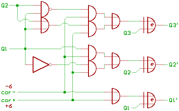
Now for something different: 7485 magnitude comparators.
Since availability of 74F85 and 74AC85 doesn't look good, this posting won't be useful for _this_ project,
but maybe somebody could turn the concept into something useful later in the future (you never know).

Be warned, that it's all untested... and just theory.
Might contain some errors, don't expect things to work at first try.

;---

While flipping through the pages of the 1985 Fairchild 74F data book at Bitsavers,
the picture on page 4-29 (page 74 of the PDF) about cascading 74F85 magnitude comparators had caught my attention:

Attachment:
7485_fairchild.png
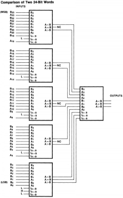
7485_fairchild.png [ 71.97 KiB | Viewed 2897 times ]


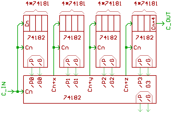
It somehow reminded me to cascading 74182 carry lookahead chips:

Image

;...

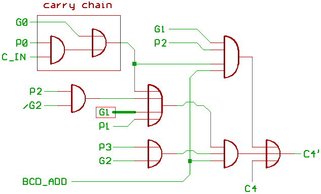
7485 is optimized for speed, so it isn't obvious from the gate level schematic in the 7485 datasheet,
but when drawing a (slower) Bit_sliced version of a magnitude comparator, I'm getting something like this for a single Bit:

Attachment:
7485_slice.png
7485_slice.png [ 174.06 KiB | Viewed 2897 times ]


The light_blue marked part is the logic which detects A>B, and when re_drawing that part a few times,
it appears to be just subtractor circuitry calculating A-B by inverting B (similar to how SBC works in the 6502 ALU).

;...

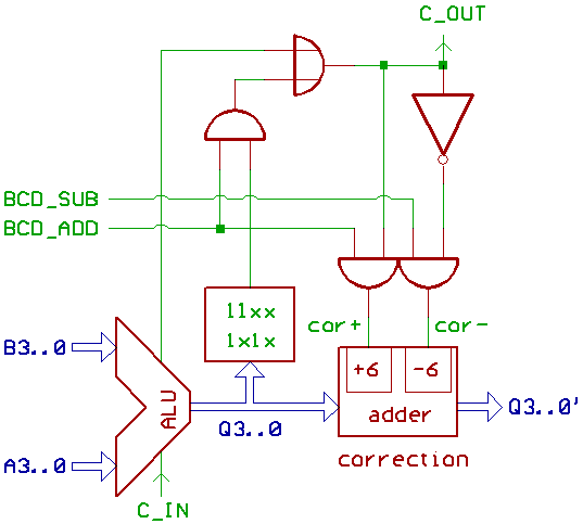
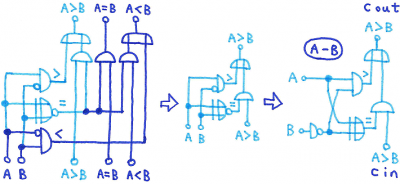
So when we have a 4 Bit adder, and we want to build a 4 Bit carry lookahead circuitry for the adder carry output,
in theory we could just take a 7485 magnitude comparator and invert the comparator B input:

Attachment:
7485_adder.png
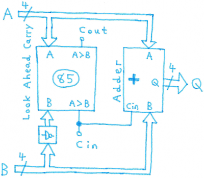
7485_adder.png [ 152.56 KiB | Viewed 2897 times ]


;....

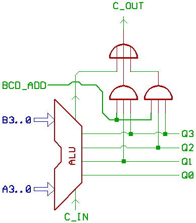
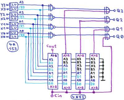
Now for a (hypothetical) 4 Bit ALU, with a 7485 based carry chain:

Attachment:
7485_alu.png
7485_alu.png [ 394.97 KiB | Viewed 2897 times ]


The boxes labeled "LU" are logic units based on 74153 4:1 multiplexers.


Top
 Profile  
Reply with quote  
PostPosted: Fri Jun 07, 2019 12:10 am 
Offline
User avatar

Joined: Sun Oct 18, 2015 11:02 pm
Posts: 428
Location: Toronto, ON
Work on the C74-6502 Rev B continues ...

At this point, I’ve looked over most aspects of the new design, and a significant speed hike seems indeed feasible. Several factors are contributing to the improvement:

  • Pre-loading input data (Decode Phase)
  • WriteFlags pipeline stage
  • FET Switch Adder
  • RAM microcode store
  • 3.3V LVC components

Given that, it’s time to start thinking seriously about signal integrity. Edge-rates will not be any faster, but I am assuming here that a faster clock will allow less time for reflections to die down, and errors may start to creep-in on latching inputs. So the question is, what’s a reasonable trace length to work to?

I spent a few minutes googling around to try to figure it out. Here is what I found:

So, after some searching, I end up with a range of 4” to 21”, which is too broad a range to be useful. :roll:

I may be able to get this new design onto a single densely populated Eurocard-sized PCB (by using TSSOP rather than SOIC parts). But even then, keeping all traces shorter than 4” to be on the safe side is going to be very difficult. If the CPU works as expected, we might see clock speeds above 50MHz. Termination on clock signals will likely be required, but other traces may need to be terminated as well. Unfortunately, short of ordering some test PCBs to check things out, I’m not sure how to get a feel for the tolerances here.

_________________
C74-6502 Website: https://c74project.com


Last edited by Drass on Fri Jun 07, 2019 11:00 pm, edited 1 time in total.

Top
 Profile  
Reply with quote  
PostPosted: Fri Jun 07, 2019 2:07 am 
Offline
User avatar

Joined: Fri Aug 30, 2002 1:09 am
Posts: 8428
Location: Southern California
See the applicable section of the 6502 primer "Construction: Avoiding AC-Performance Problems," at http://wilsonminesco.com/6502primer/construction.html and the links there, including to a couple of forum topics.

Terminations assume the transmission-line impedance is controlled. If the terminating resistance is not near the characteristic transmission-line impedance, it won't really do any good. Schottky diode terminations work well if you can find diodes that are fast enough; but I don't know where you'll find any fast enough for this.

_________________
http://WilsonMinesCo.com/ lots of 6502 resources
The "second front page" is http://wilsonminesco.com/links.html .
What's an additional VIA among friends, anyhow?


Top
 Profile  
Reply with quote  
PostPosted: Fri Jun 07, 2019 8:45 am 
Offline
User avatar

Joined: Fri Nov 09, 2012 5:54 pm
Posts: 1392
The fastest Schottky diode I know is the LL101, trr=1ns.

Schottky diode arrays from TI:
SN74F1016 16 Bit Schottky diode plus R-C bus termination array, trr=8..10ns
SN74S1053 16 Bit Schottky diode bus termination array, trr=8..16ns
SN74S1051 12 Bit Schottky diode bus termination array, trr=8..16ns
SN74F1056 8 Bit Schottky diode bus termination array, trr=5..7ns

There are smaller Schottky diode arrays, for instance the 3 pin BAT54SW, trr_max=5ns

It's an interesting question, if TVS diode arrays could be used for line termination, too.
Vishay VBUS54GD-FBL, 4 line ESD protection for HDMI,SATA, etc. (don't ask me how to solder that package).

;---

Edit1:
1972 Motorola System Design Handbook has something on page 82 about "Schottky Diode Termination".
Also interesting: page 109, Multilayer ECL board layouts.

The MBD101 Schottky diode used for line termination in the Motorola handbook still is available and in production
as MMBD101 in SOT23 SMD package.

MBD101 seems to have less capacitance than the LL101.

;---

Edit 2:
MMBD352 'Dual Hot Carrier Mixer Diode', the datasheet looks interesting.
MMBD352TL1,SOT-23 (TO-236) package.
MMBD352WT1,SOT-323 (SC-70) package.


Last edited by ttlworks on Tue Jun 25, 2019 6:27 am, edited 2 times in total.

Top
 Profile  
Reply with quote  
PostPosted: Fri Jun 07, 2019 6:58 pm 
Offline
User avatar

Joined: Sun Oct 18, 2015 11:02 pm
Posts: 428
Location: Toronto, ON
Ah, so much to learn, so much to learn ... thanks for the links gents.

I understand that controlled impedance requires that several parameters be managed carefully, including the geometry of the trace itself, the distance to the reference plane, the dielectric material, and so on. Then there are vias and connectors to further complicate matters. There are a few calculators around to figure things out, and I understand also that one can spec the target impedance for traces and the board house will adjust things slightly as required (which sounds very expensive).

Interestingly, I note some LVC family ICs have series resistors built-in on outputs (25Ω for 74LVCR2245s fore example), so I suppose source termination is common enough out there. My hope is to try to keep traces short enough to not have to worry about any of this, but I have a feeling “some restrictions will apply” nevertheless. :(

_________________
C74-6502 Website: https://c74project.com


Top
 Profile  
Reply with quote  
PostPosted: Fri Jun 07, 2019 10:28 pm 
Offline
User avatar

Joined: Fri Dec 12, 2008 10:40 pm
Posts: 1000
Location: Canada
ttlworks wrote:
Since availability of 74F85 and 74AC85 doesn't look good,...


How about 74F521 comparators? They are 8 bit, but only show equal or /equal. No > or <.

Or configuring 7ns GAL22V10s as magnitude comparators?

_________________
Bill


Top
 Profile  
Reply with quote  
PostPosted: Sat Jun 08, 2019 1:13 am 
Offline
User avatar

Joined: Sun Oct 18, 2015 11:02 pm
Posts: 428
Location: Toronto, ON
I thought I would share the (very rough) block diagram I’m working with for the new design.
Attachment:
11B03BAA-4F06-49E4-90DB-EDD0E3109BCD.png
11B03BAA-4F06-49E4-90DB-EDD0E3109BCD.png [ 178.76 KiB | Viewed 2778 times ]
Some optimizations to note:
  • The ALU inputs are registered (ALUA, ALUB and ALUC). They are pre-loaded in the cycle prior to the ALU operation.
  • The transparent latch (ALUR) at the output of the ALU, prior to the Flags logic, allows the BRanch test logic and writes to the P register to be executed in the cycle following the ALU operation (WriteFlags pipeline stage).
  • Inverting and non-inverting buffers work in parallel to connect the Data Bus to the ALUB input. A byte read from memory can therefore be inverted in the cycle prior to an SBC operation at no extra cost, thereby eliminating the need for inverters in the ALU itself.
  • ADL/ADH and R/W are registered as well, and are also pre-loaded in the cycle prior to their use.

As with the prior version, microcode is prefetched. The new Decode logic (not shown) enables the CPU to pre-load input registers, and otherwise get a jump on control logic (by decoding the Opcode on the fly). The ALU Execute cycle is made shorter by pre-inverting the B input as necessary. The ALU itself is much faster through the use of a FET Switch Adder. And finally, the WriteFlags pipeline stage takes care of all post-ALU processing.

Taken together, these improvements should make for lots of parallel processing and a much shorter critical path. We’ll have to see whether the concept holds up. :)

_________________
C74-6502 Website: https://c74project.com


Top
 Profile  
Reply with quote  
PostPosted: Fri Jun 14, 2019 8:11 am 
Offline
User avatar

Joined: Fri Nov 09, 2012 5:54 pm
Posts: 1392
74377 is an exotic chip.
It's worth a thought if we could pick up an old idea from Jeff: building registers from 74163 4 Bit counter chips instead of using the 74377.

Hey, maybe we even could toss that 74283 based 16 Bit incrementer out of the design.

Would suggest to take a look at the 65CE02 block diagram:

Attachment:
65CE02_blockdiagram.png
65CE02_blockdiagram.png [ 198.28 KiB | Viewed 2730 times ]


Top
 Profile  
Reply with quote  
PostPosted: Tue Jun 18, 2019 5:41 am 
Offline
User avatar

Joined: Fri Nov 09, 2012 5:54 pm
Posts: 1392
BillO wrote:
How about 74F521 comparators?

74F521 is just an identity comparator like the 74688, no subtractor circuitry inside.
Something like 74AS885 would be better.
Using GAL22V10 would be cheating. ;)

Anyhow, it looks like a carry chain built from FET 2:1 multiplexers\switches would be quite the thing.
Building a carry chain from individual transistors was "plan B", comparators "plan C".

;---

Did a search for counters with three_state outputs, TI and OnSemi, but the results don't look good.

74AS869 8 Bit up/down counter with three_state outputs is a neat chip, but for 50MHz it's too slow.

;---

Edit:
When comparing the NXP 74LVC163 counter wired up as a latch and the NXP 74LVC377 latch,
74LVC163 has slightly less propagation delay than the 74LVC377 (clock to data output),
74LVC377 needs slightly less setup time than the 74LVC163 (data and control input to clock).


NXP 74LVC163 4 Bit counter: VCC = 3.0V .. 3.6V, -40°C .. +85°C
tsu setup time: Dn to CP = 2.5ns_max 1.0ns_typ; /PE to CP = 3.0ns_max 1.2ns_typ
tpd propagation delay: CP to Qn = 1.5ns_min 3.8ns_typ 7.3ns_max

NXP 74LVC377 8 Bit latch: VCC = 3.0V .. 3.6V, -40°C .. +85°C
tsu setup time: Dn to CP = 2.0ns_max 0.7ns_typ; /E to CP = 3.0ns_max 0.2ns_typ
tpd propagation delay: CP to Qn = 1.5ns_min 4.0ns_typ 7.6ns_max


Top
 Profile  
Reply with quote  
PostPosted: Thu Jun 20, 2019 1:13 am 
Offline
User avatar

Joined: Fri Aug 30, 2002 1:09 am
Posts: 8428
Location: Southern California
The 74_181 keeps coming up, so I thought I'd link to this article:
Inside the vintage 74181 ALU chip: how it works and why it's so strange
http://www.righto.com/2017/03/inside-vi ... ow-it.html
(Someone posted the link on the MoHPC HP calculator forum.)

_________________
http://WilsonMinesCo.com/ lots of 6502 resources
The "second front page" is http://wilsonminesco.com/links.html .
What's an additional VIA among friends, anyhow?


Top
 Profile  
Reply with quote  
PostPosted: Fri Jun 21, 2019 5:08 am 
Offline
User avatar

Joined: Fri Nov 09, 2012 5:54 pm
Posts: 1392
74181 ?
Been there, done that. (page 3, 4, and 5)

Another interesting (but more exotic than the 74181) TTL ALU chip would be the 74381.

Project5474 is about reverse engineering TTL chips, but progress seems to be slow.

There is a detailed AM2903 dissection from 1979.
//AM2903 was a 4 Bit bitslice chip from AMD, containing an ALU and registers.


Top
 Profile  
Reply with quote  
PostPosted: Wed Jun 26, 2019 1:05 pm 
Offline
User avatar

Joined: Fri Nov 09, 2012 5:54 pm
Posts: 1392
The BCD circuitry in our old TTL CPU design appears to be a bottleneck when trying to go faster than 20MHz.

There is an old article about BCD correction in the NMOS 6502, the interesting part starts here.

Our old TTL CPU design uses 74283 adders for BCD correction.
74283 isn't too fast.
NMOS 6502 does the correction without resorting to an adder:

Image

Edit: cor+ and cor- in the picture above might be generated this way:

Image

Now to make creative use of the 74LVC1G99 (which happens to have an output enable) for building a BCD correction:

Attachment:
bcd_corr_1g99.png
bcd_corr_1g99.png [ 250.89 KiB | Viewed 2513 times ]


Q0 doesn't need to be corrected.
C4 is the ALU carry output, C4' is the carry output after the $A..$F detection.

That 74151 gated with the ALU carry output just detects $A..$F at the ALU output during decimal ADC, nothing fancy there.
Works like this:

Image

Image

Since the 74AC151 worst case timing is agonizingly slow, another approach for detecting $A..$F at the ALU output would be making creative use of fast FET switches
(that sort of switches we would like to use for implementing the carry chain inside the ALU):

Attachment:
bcd_det_qfetsw.png
bcd_det_qfetsw.png [ 68.07 KiB | Viewed 2513 times ]


Last edited by ttlworks on Thu Jun 27, 2019 7:51 am, edited 1 time in total.

Top
 Profile  
Reply with quote  
PostPosted: Wed Jun 26, 2019 1:16 pm 
Offline
User avatar

Joined: Fri Nov 09, 2012 5:54 pm
Posts: 1392
Of course, detecting $A..$F at the ALU output isn't the end of the ladder,
NMOS 6502 makes creative use of the propagate\generate signals inside the ALU instead.

An oversimplified and not 100% technically exact picture of how the NMOS 6502 does it:
//The red box _could_ be a part of the carry chain, but in the NMOS 6502 chip layout, it isn't.

Image

After omitting the BCD_ADD (ADC BCD) signal for better reliability, I'm getting this:

Attachment:
bcd_det_nmos6502.png
bcd_det_nmos6502.png [ 80.29 KiB | Viewed 2509 times ]


When tinkering a bit with an old test program, I'm getting an alternative approach:

Attachment:
bcd_det_alternative.png
bcd_det_alternative.png [ 87.91 KiB | Viewed 2509 times ]


Top
 Profile  
Reply with quote  
PostPosted: Thu Jun 27, 2019 7:54 am 
Offline
User avatar

Joined: Fri Nov 09, 2012 5:54 pm
Posts: 1392
And when tinkering with the alternative form of the $A..$F detection,
an implementation of it by resorting to FET switches would look like this:

Attachment:
bcd_det_pgfetsw.png
bcd_det_pgfetsw.png [ 135.81 KiB | Viewed 2474 times ]


And an implementation resorting to multiplexers would look like that:

Attachment:
bcd_det_pgmux.png
bcd_det_pgmux.png [ 122.79 KiB | Viewed 2474 times ]


Top
 Profile  
Reply with quote  
PostPosted: Thu Jun 27, 2019 12:30 pm 
Offline
User avatar

Joined: Sun Oct 18, 2015 11:02 pm
Posts: 428
Location: Toronto, ON
This is really great Dieter! I’ll take a closer look at the [$A..F] Detect circuits.

I made a few mods to the BCD Adjust circuit above. The propagation delay is reduced significantly if we use FET Multiplexers for the adjust logic, as follows:
Attachment:
5E87B0E1-F7A8-4CE6-825E-3B03D6466A82.jpeg
5E87B0E1-F7A8-4CE6-825E-3B03D6466A82.jpeg [ 21.89 KiB | Viewed 2452 times ]
In this diagram, BCDLC and /BCDLC are the positive and negative outputs of the [$A..$F] Detect ‘151. They are connected to the Data Inputs of the subsequent FET Muxes. The Select Inputs take much longer to resolve, and use only signals which are available already by the time BCDLC arrives. The switching time of the MUXes is therefore taken out of the critical path. :D

I managed to test the adjust circuits in Logisim, and they both check out — good news.

Cheers!

_________________
C74-6502 Website: https://c74project.com


Top
 Profile  
Reply with quote  
Display posts from previous:  Sort by  
Post new topic Reply to topic  [ 149 posts ]  Go to page Previous  1, 2, 3, 4, 5, 6, 7 ... 10  Next

All times are UTC


Who is online

Users browsing this forum: No registered users and 22 guests


You cannot post new topics in this forum
You cannot reply to topics in this forum
You cannot edit your posts in this forum
You cannot delete your posts in this forum
You cannot post attachments in this forum

Search for:
Jump to: