Now for tossing in something different:
Somewhere up in the thread, we had a few words about how difficult the 6502 instruction decoding is,
and this had brought me to the idea of playing the "what if" game:
6502 has a 16 Bit address bus and an 8 Bit data bus, and that's what adds a lot to the complexity of the 6502.
What, if the address bus _and_ the data bus for a "6502 styled CPU" would be both 16 Bit ?
Had tinkered for a week with this idea, and here the results:
Attachment:
 m16_mill.png [ 145.27 KiB | Viewed 2402 times ]
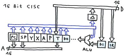
PC is a 16 Bit counter, all the other registers are just registers.
The blue shaded registers are not visible to the end user.
The blue bus line is the internal data bus of the CPU.
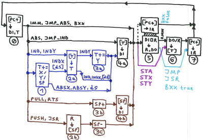
Now for the state machine diagram:
Attachment:
 m16_state_diagram.png [ 331.59 KiB | Viewed 2402 times ]
No more zero page addressing, but all the other addressing modes seem to be there
(just had to add stack relative data and pointers, you sure can imagine how to implement
stack relative pointer with Y register as an offset).
For Bxx false, the ALU does nothing in step 5 while the next instruction word is fetched,
for BXX true the 16 Bit immediate value fetched in step 0 is added to PC in step 5.
Compare this to a rapid transit map:

In step 5, the train is at the station, and "something" happens to the chargo (data).
Adding PEA, PEI and PER to the state machine diagram is left as a homework assignment to the experienced reader.
Point is: we now have a 16 Bit instruction word,
and if one would be using mostly the lower part of the instruction word for controlling the sequencer (telling it which steps to skip),
while using most of the upper part of the instruction word for controlling ALU, registers and flags in step 5,
the layout of the opcode map somehow would resemble a bit the layout of the opcode map of the 6502.
For a 65C02 (and for our TTL CPU), a state machine flow diagram would be at least 4 times as big,
and a lot more complicated because a 16 Bit address has to be calculated with an 8 Bit ALU,
one needs to test for edge cases like page crossings etc.
When trying to implement an instruction decoder\sequencer for the 65C02 functionality plus some extras
by using 74138 decoders, 74151 multiplexers and logic chips, I think this would take more than 150 chips in total,
limiting the speed of a design which has a 2 level pipeline to maybe less than 10 MHz.
;---
Downside of the state machine flow diagram is, that all of the instructions take at least two memory words and two machine cycles.
If one would add a little bit logic which detects single word instructions in step 0, then prevents that PC+ is written into PC at the end of cycle 0 if this is the case
(like in the NMOS 6502 and in our TTL CPU), single word instructions would work, but they still take two machine cycles.
Questions to Drass:
First:
We currently seem to generate the control signals for step 0 by hardware.
If _all_ of the microcode sequences would contain that [PC+] read for step 0, is there a chance for simplifying this circuitry ?
Second:
We now do ALU operation and flag evaluation in the EXECUTE machine cycle.
In which cycle the status register P is pushed on stack when the CPU responds to an interrupt ?
In theory, it might be possible to do just the ALU operation in the EXECUTE machine cycle, while latching the ALU outputs into a temporary register
for doing the flag evaluation and the status register update in the machine cycle that follows EXECUTE.
But I think this would complicate implementing cycle exact BXX false.


