6502.org Forum  Projects  Code  Documents  Tools  Forum
It is currently Fri May 24, 2024 6:03 pm

All times are UTC


Post new topic Reply to topic  [ 149 posts ]  Go to page Previous  1 ... 6, 7, 8, 9, 10  Next
Author Message
PostPosted: Fri Aug 16, 2019 6:20 am 
Offline
User avatar

Joined: Fri Nov 09, 2012 5:54 pm
Posts: 1394
Nah, it's just another paper design.

I happen to have about two cubic meters of old scratch paper somewhere in the basement,
pages are either labeled "obsolete", "rejected", "won't work" or "done".

In case of emergency, this would bring me through a cold winter. ;)

Image

The mightiest design tools known to men are paper, pencil and common sense.
Unfortunately they are the slowest design tools, so one can't affort resorting to them in an engineering job nowaday...
...but since it's just a hobby project, here we go.


Top
 Profile  
Reply with quote  
PostPosted: Fri Aug 16, 2019 6:56 am 
Offline
User avatar

Joined: Fri Nov 09, 2012 5:54 pm
Posts: 1394
So I had started this way:

Attachment:
helios1.png
helios1.png [ 362.95 KiB | Viewed 1329 times ]

Attachment:
helios2.png
helios2.png [ 77.55 KiB | Viewed 1329 times ]


If the CPU would only do data calculations, it would have a higher bus bandwidth,
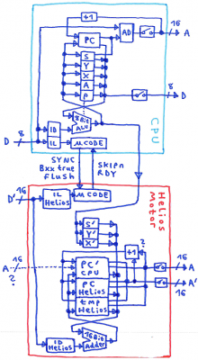
to compensate for this the Helios Motor would need a 16 Bit data bus (plus interleaved memory):
for being able to fetch 16 Bit pointers from program memory, zero page and stack.

A few things in the block diagram are not worked out well,
mainly because they don't need to be worked out well now. :lol:
Just watch out for question marks in the block diagram.

In case of JMP\JSR and Bxx taken, the 16 Bit incrementer in the CPU would need to be able to read an address from the address bus.
Considering the bus capacitances, this would affect the reliability of the design pretty much, but it's just a Gedankenexperiment anyhow.
//Physicist Schrödinger in the PC repair shop: my PC is working and not working at all, I'm happy and very disappointed.

The Helios Motor has a 16 Bit address adder, if we do flag evaluation in the Helios Motor
it isn't related to the ALU output like in the CPU,
it's for marking/flagging/categorizing valid pre_emptive address calculation results.

The CPU needs to tell the Helios Motor:
SYNC, I'm doing the next instruction fetch.
flush, forget the pre_calculated results because I'm taking an interrupt or such.
Bxx true, my PC needs new contents.

The Helios Motor needs to tell the CPU:
RDY, wait because I'm falling behind.
SKIPn, skip soandsomuch steps of microcode.

;---

My next thought was: what, if disconnecting the CPU from the address bus, and generating the CPU address output inside the Helios Motor instead ?

;---

Then I remembered Jeff's KimKlone.
It would simplify things a great deal if the Helios Motor would be able to send fake instruction Bytes into the CPU.

The Helios Motor is one instruction ahead of the CPU, so if it senses a "LDA ABS",
it could fake a "LDA #" instruction to the CPU, then place the address on the address bus in the right moment when the CPU reads data.

A "STA ABS" then would result in a faked "STA Z" for the CPU.

;---

After doing some math, it appeared to me that with a Helios concept like in the block diagram,
most instructions in the CPU would take two cycles, so we can't go past 50MIPs at 100MHz anyway.

Original 6502 architecture would be 43MIPs at 100 MHz,
and for the amount of chips required for building a Helios Motor, that's "Meh".

So I switched back to "monolithic view". :lol:

A conventional TTL CPU, plus a "hardware upgrade kit" containing a 16 Bit address adder and some additional stuff.

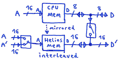
Modified Harvard design:
one bus system (8 Bit) for data,
one bus system (16 Bit) (interleaved memory) for instructions plus 16 Bit pointers in zero page and stack.

Something like a 6 level pipeline,
where the first half of the pipeline focuses on instruction predecoding and pre_emptive address calculations,
and the second half of the pipeline focuses on detailed instruction decoding and data calculations.

Breaking instruction decoding in two parts, address calculation and data calculation: pipelined instruction decoding that is.

Let's call it the Helios CPU. :lol:

Anyhow, when trying to do more than one instruction per machine cycle, it would be close to impossible
to get around having something in the CPU hardware that somehow resembles Harvard architecture and VLIW.

;---

Edit:
Non_monolithic mode:

If the Helios motor would be able to take over the CPU instruction decoder, for controlling microcode execution in the CPU
and initiating a data calculation without that this causes traffic on the CPU data bus,
the Helios block diagram still might be working, and when doing it right in theory something like 90MIPS at 100MHz might be possible.

Hmm...
Decisions, decisions.


Top
 Profile  
Reply with quote  
PostPosted: Fri Aug 16, 2019 10:09 am 
Offline
User avatar

Joined: Fri Nov 09, 2012 5:54 pm
Posts: 1394
Now to take a break.

Since Harward design and VLIW went mentioned up in the thread, now for some shark tourism.

The only VLIW RISC I had tinkered with was the ADSL21065L, but it's been many years ago,
and it appears that some of my memory about the technical details isn't too correct.

ADSP21065L user's manual
ADSP21065L technical reference

Attachment:
ADSP21065L_blockdiagram.png
ADSP21065L_blockdiagram.png [ 95.35 KiB | Viewed 1311 times ]


ADSP21065L was designed for digital signal processing in the first place (only 32 Bit integer and 40 Bit floating point supported),
but with the help of a C compiler it also could do a good job as a "general purpose microcontroller".
//When defining a variable as char, int or long, the compiler stubbornly made it 32 Bit.

IIRC a lot of the VLIW instruction words could be conditional.
In addition to the usual set of jumps\calls and conditional branches,
there is a set of jumps\calls and conditional branches which take effect after two more instructions to prevent empty slots in the pipeline.

Two bus systems, one for instructions (48 Bit) and data (32 Bit \ 40 Bit or such).
One "data address generator" (DAG) feedig the address bus of one bus system.
Two RAM blocks on chip.

An ALU with a neat register file, and two address generators feeding the two bus systems.
//I'm leaving out a few details here, for instance that hardware multiplier.

Digital filtering seems to circle around multiplying a set of variables with a set of constants while accumulating the results,
and for this purpose the SHARC architecture makes a lot of sense.

Address generators are powerful beasts.
They support Bit reversed addressing (for FFT calculations) and circular buffers anywhere in memory and at a variable size,
but since a 6502 isn't supposed to do fast FFT calculations and a 256 Bytes circular buffer simply could be implemented
by resorting to LDA ABS,X and STA ABS,X just ignore those two features (plus the related L and B registers).

Address generators are looking like this:

Attachment:
ADSP21065L_DAG.png
ADSP21065L_DAG.png [ 34.94 KiB | Viewed 1311 times ]


If SHARCs have I\O pins, some of them tend to show up in the status register and could be tested like flags.
Might be neat for "Bit banging".
//That 65C02 /SO pin...

;---

ADSP21605 belongs to the first generation of SHARCs.
Nowaday, ADSP-SC573 contains two SHARC+ cores and an ARM core.
Blackfin is an outgrew of the SHARC architecture, supporting only fixed point, but 8 Bit \ 16 Bit \ 32 Bit data types (and SIMD).

//It's interesting to see, how certain function blocks of the Helios would map to the SHARC architecture, isn't it ?
Now to depart from the sharks again...


Top
 Profile  
Reply with quote  
PostPosted: Fri Aug 16, 2019 10:30 am 
Offline
User avatar

Joined: Fri Nov 09, 2012 5:54 pm
Posts: 1394
Found an old introduction from Philips Semiconductors about the basics of VLIW,
comparing CISC and RISC to VLIW.

Attachment:
philips_VLIW.png
philips_VLIW.png [ 33.9 KiB | Viewed 1306 times ]


Nice reading material.
And with that, I think the thread now contains enough material to make the VLIW concept a little bit more clear.

//That was the last part required for mounting together that bucket wheel excavator. ;)

;---

Edit: two more links:

Carnegie Mellon College of Engineering
Lecture on VLIW

MIT Computer Science & Artificial Intelligence Lab
Compiling for EDGE (Explicit Data Graph Execution) Architectures

;---

Edit2:

Bernd Paysan's 4stack VLIW Forth CPU, that's an interesting concept:

Attachment:
4stack.png
4stack.png [ 39.45 KiB | Viewed 1156 times ]


Last edited by ttlworks on Tue Aug 20, 2019 5:07 am, edited 2 times in total.

Top
 Profile  
Reply with quote  
PostPosted: Sat Aug 17, 2019 8:28 pm 
Offline
User avatar

Joined: Sun Oct 18, 2015 11:02 pm
Posts: 428
Location: Toronto, ON
As we continue to look at alternative architectures (VLIW wow!), I wanted to caveat that we may not yet be at the limit of the current one. The still-on-paper-design *should* deliver a 100MHz clock-rate, with the key enhancements being a 4-stage pipeline and a fast FET Switch Adder. But this design is still cycle-accurate. If we are prepared to change the cycle-count, then perhaps we might look at a deeper pipeline.

The simplest approach is to break up the critical path into further pipeline stages, and re-balance the workload around the shorter cycle. The main candidates for this treatment are really three: (1) The ALU, (2) memory reads, and (3) microcode fetches. The reality is that synchronous RAM is very fast, so fetching from either external memory or the microcode store is not likely to be a bottleneck. The implication, therefore, is that a multi-cycle adder may be best the source of potential gains.

This is sort of the reverse of a wider data path. Rather than implementing a 16-bit adder to gain speed, we instead go with a 4-bit adder, and stretch the ADD operation over two cycles. (There is the temptation to implement a faster 8-bit adder with RAM, but we won’t go there). The biggest penalty of this approach is likely to arise during address calculation (indexed addressing in particular). But, we can pull the same trick that the 6502 does to skip a cycle on a clear carry; this time applied at the level of a nibble. Some portion of time at least, there will be no nibble carry, and indexed addressing can take the same number of cycles as before. And if not, then perhaps we may yet skip the final nibble and still save a cycle from the worst case.

Honestly, it’s difficult to quantify the gains from this change (and I’m not altogether certain that the approach works). But it seems promising. The actual gain will depend on the mix of instructions in the program being executed. If we assume that a 4-bit adder allows a 1/3 reduction in the critical path over an 8-bit adder (which seems likely), then we would incur at worst the equivalent of a 2/3 cycle penalty for adder operations which have to be fully resolved across 16-bits (i.e. a carry is generated for all of the three high-order nibbles). Meanwhile, all other cycles are faster by 1/3.

So, with a reasonably favourable opcode stream, we may get something approaching a 30% performance boost with relatively little extra hardware. We should note, however, that a specifically unfavourable opcode stream may do worse; a series of absolute indexed ADC instructions, for example, will take a 6.5% performance hit if all nibble boundaries are tripped every time (adr_lo, adr_hi and the add itself all take an extra cycle, so 8 * 2/3 cycles vs. 5 cycles).

It’s worth noting that other instructions would be allowed to continue executing during the hi-nibble-adder cycle in a conventional a pipeline. In this case, however, we would simply stall the pipeline unconditionally. We forfeit some throughput as a result, but we also avoid complex logic to detect dependencies; a significant benefit in this case.

One issue that arises here is how to manage a 16-bit PC increment within the 1/3 shorter cycle. An incrementer is faster than a general purpose adder, but this is 16 bits to 4. There are other problems as well, like address decoding (and I could easily be missing several). Nevertheless, I thought it worthwhile to share this as yet another approach to explore.

_________________
C74-6502 Website: https://c74project.com


Top
 Profile  
Reply with quote  
PostPosted: Sat Aug 17, 2019 8:47 pm 
Offline
User avatar

Joined: Thu Dec 11, 2008 1:28 pm
Posts: 10804
Location: England
Isn't a faster adder design (or indeed a faster incrementer) worth exploring? We know that the 6502's incrementer has some carry lookahead. And we know that there are faster adder implementations than ripple carry...


Top
 Profile  
Reply with quote  
PostPosted: Sat Aug 17, 2019 10:18 pm 
Offline
User avatar

Joined: Sun Oct 18, 2015 11:02 pm
Posts: 428
Location: Toronto, ON
BigEd wrote:
Isn't a faster adder design (or indeed a faster incrementer) worth exploring?
It certainly is. I’m working on a test PCB to exercise the current implementation, so we’ll see how it performs. One likely improvement is to divide the FET Carry chain into 4-bit segments to lower capacitance and improve propagation. So far as I can tell, Generate and Propagate carry-lookahead signals take too long, relative to the FET carry chain, to be of much benefit (but I may be missing something there).

_________________
C74-6502 Website: https://c74project.com


Top
 Profile  
Reply with quote  
PostPosted: Sun Aug 18, 2019 11:02 am 
Offline

Joined: Mon May 21, 2018 8:09 pm
Posts: 1462
In the address calculations of the '816, it is sometimes necessary to add three numbers together - the DPR or SP, an index register, and an offset operand. I think there may be more benefit to combining this into a single optimised unit, thereby reducing cycle count, than speeding up single additions to make each cycle faster. In such a case, you are aided by the fact that low-order bits become valid sooner than high-order bits in the worst case, *and* low-order bits are *needed* sooner. You can therefore incur the carry propagation penalty only once for both adders. (Also, the resulting address is only 16 bits wide, so the carry chain is shorter than for a long indexed address.)

In a related case, it is often necessary to produce sequentially related addresses for a single operation (instruction fetching, indirect addressing, stacking and unstacking addresses, and on entering or leaving an ISR). This can be at most 3 sequential addresses on the 6502, and at most 4 on the '816. The likelihood that one of these increments or decrements will incur a long carry chain rises proportionately - but at most one will do so within a given sequence.

Of course, the single most obvious benefit realisable from dropping cycle accuracy is that simple implicit-mode instructions can be single cycle. These can be a substantial component of loop overhead in performance-critical code. I understand the 65CE02 took advantage of that idea, but it seems to be a pretty rare chip.


Top
 Profile  
Reply with quote  
PostPosted: Mon Aug 19, 2019 1:38 am 
Offline

Joined: Thu Mar 10, 2016 4:33 am
Posts: 169
If the requirement to be cycle accurate is removed then there are quite a few opportunities for speeding up instructions. I think the 65CE02 did this to good effect. One byte instructions execute in 1 cycle, and the extra cycle for page boundary carry propagation was also removed, reportedly resulting in quite a good speed improvement.

Mitsubishi and Rockwell also added multiply instructions. Rockwell also added mutiply-accumulate. This should result in a large speed improvement for code that can make use of the multiplier without any need for architectural changes.

It would also be nice to have a 65C816 chip with all the address pins exposed and a 16-bit data bus. This would complicate the external bus a bit but could be done quite easily if the internals were kept the same, but an even better improvement would result if the internal busses were also 16-bits. The '816 is still mostly an 8-bit chip inside.


Top
 Profile  
Reply with quote  
PostPosted: Mon Aug 19, 2019 11:32 pm 
Offline
User avatar

Joined: Sun Oct 18, 2015 11:02 pm
Posts: 428
Location: Toronto, ON
Chromatix wrote:
In the address calculations of the '816, it is sometimes necessary to add three numbers together - the DPR or SP, an index register, and an offset operand. I think there may be more benefit to combining this into a single optimised unit, thereby reducing cycle count, than speeding up single additions to make each cycle faster. In such a case, you are aided by the fact that low-order bits become valid sooner than high-order bits in the worst case, *and* low-order bits are *needed* sooner.
Thanks for the comment Chromatix. I’m not quite sure how to take advantage of the lower-order bits coming out sooner. Can you elaborate?

Quote:
In a related case, it is often necessary to produce sequentially related addresses for a single operation (instruction fetching, indirect addressing, stacking and unstacking addresses, and on entering or leaving an ISR). This can be at most 3 sequential addresses on the 6502, and at most 4 on the '816. The likelihood that one of these increments or decrements will incur a long carry chain rises proportionately - but at most one will do so within a given sequence.
That’s a helpful insight. Dieter suggested up-thread that a wider adder (or incrementer) would make for some efficiencies along these lines. There is a tradeoff between width and speed, so we’ll have to see how the FET adder tests work out.

Quote:
Of course, the single most obvious benefit realisable from dropping cycle accuracy is that simple implicit-mode instructions can be single cycle. These can be a substantial component of loop overhead in performance-critical code. I understand the 65CE02 took advantage of that idea
I agree. Reducing DEY, for example, from two cycles to one makes a lot of sense. The pipeline can accomplish this by “forwarding” the opcode from redundant FetchOperand cycle directly to the DECODE stage of the pipeline. It’s a good idea and probably “doable” with the existing pipeline.

Quote:
the 65CE02 did this to good effect. One byte instructions execute in 1 cycle, and the extra cycle for page boundary carry propagation was also removed, reportedly resulting in quite a good speed improvement.
Thanks for the feedback jds. Looks like the 65CE02 is a good model here. The Wikipedia page suggests these two improvements led to a 25% gain in throughput at a given clock-rate. Definitely worth considering. :)

_________________
C74-6502 Website: https://c74project.com


Top
 Profile  
Reply with quote  
PostPosted: Tue Aug 20, 2019 12:20 am 
Offline

Joined: Mon May 21, 2018 8:09 pm
Posts: 1462
What I mean is that the low-order bits are both valid sooner at the output of the first adder, and the most critical for timing at the input of the second adder, which is a useful coincidence that makes the total latency of two consecutive adders less than twice that of a single adder. When trying to optimise the cycle count of a relatively complex address calculation, one which seems to be pretty common on the '816 (Direct Page Indexed accesses would use it, as the local equivalent of the 6502's Zero Page Indexed), this seems like a useful property to help keep the clock rate up at the same time.

Since one of the operands of this three-way addition would come from the instruction stream, it seems reasonable to assume that the sum of the index register and the DPR should be initiated first, and the offset operand applied to the second adder stage. The result is a 16-bit address in Bank Zero.

The other critical address calculation on the '816 is one that results in 24-bit addresses, but only two operands need to be added and one of these is only 16 bits wide. The bank byte thus only needs an optional increment operation, not a complete adder. Intuitively, I would guess this takes about as long as the two consecutive 16-bit adders.


Top
 Profile  
Reply with quote  
PostPosted: Tue Aug 20, 2019 5:29 am 
Offline
User avatar

Joined: Thu Dec 11, 2008 1:28 pm
Posts: 10804
Location: England
(If you need a quick optional increment of the bank byte, then you can always have in hand an incremented version of the bank byte, and use a mux to select the incremented version.)


Top
 Profile  
Reply with quote  
PostPosted: Tue Aug 20, 2019 6:21 am 
Offline
User avatar

Joined: Fri Nov 09, 2012 5:54 pm
Posts: 1394
Most critical for the adder timing are the propagation delays in the carry chain, because the carry chain only is one level of XOR gates away from the adder output.
I'm looking forward to seeing, how the FET switch carry chain hardware turns out. //If it's really as fast as expected, that is.
It's hard to estimate/calculate/simulate the effects of capacitances (IC pins and PCB traces) and switch resistances piling up for 8 Bits.
Depending on the outcome of the test PCB, this would open or close some possibilities for what the CPU architecture should look like.

A three way adder would require having two carry chains.
Reminds me to the game of building binary parallel multipliers and the problem of adding partial sums.
Fairchild 100K ECL Data Book, page 193 of the PDF, the F100182 9 Bit Wallace Tree Adder.

;---

For "LDA Z,X", 65816 does "8/16 Bit index register" + "8 Bit offset" + "16 Bit DPR".
K24 only does "8 Bit index register" + "8 Bit offset" + "16 Bit DPR with Bit 7..0 always zero", or short: ("8 Bit index register" + "8 Bit offset") OR "DPR with Bit 7..0 always zero".
Means, that K24 can go without a three input adder.

A (hypothetical) 65816 mode for the TTL CPU won't have to be cycle exact. Let's suppose, we only have a two input 16 Bit address adder.
One could check in the previous machine cycle, if DPR Bit 7..0 is zero, and if the index register is 8 Bit.
Then to handle that address calculation like in K24 if YES, and to insert a machine cycle for another 16 Bit addition if NO.
//It's an interesting question, what would be faster: a three input adder probably only would allow for a slower PHI2 than a two input adder,
//but a two input adder might require inserting another machine cycle for adding three variables sometimes.

Another approach would be having two shadow registers for pre_emptively calculating "DPR+X" and "DPR+Y" in a previous machine cycle.
Then to only add "DPR+X\Y" + "16 Bit offset" with a two input 16 Bit adder.
//In the cycle after an instruction fetch, the ALU of a 6502 is sitting idle.

;---

For 24 Bit address calculation, one could have shadow registers and calculate "bank register +1" one cycle ahead,
then use the carry output of the 16 Bit address adder for selecting between the output of "bank register" and "bank register +1"
for generating address Bits 23..16.
//BigEd already had suggested something like that while I was typing.

Hmm... would it make sense to have shadow registers containing "PCH +1" and "PCH -1" for speeding up conditional branches during a page crossing ? ;)

;---

The main problem here is the physical construction of the CPU.
A bigger amount of circuitry means more chips using more PCB space, resulting in longer PCB traces and more capacitances (probably slowing down the signals).

We need to be careful/selective when adding circuitry to the design, because what could make the CPU faster at logic design level might reduce CPU speed at physical level later.

But it's hard to estimate, what the "netto" speed gain/loss of an "architectural feature" might be... yet.
//Feels like that's going to be a lot of "math homework".


Top
 Profile  
Reply with quote  
PostPosted: Mon Aug 26, 2019 11:17 am 
Offline
User avatar

Joined: Sun Oct 18, 2015 11:02 pm
Posts: 428
Location: Toronto, ON
ttlworks wrote:
The main problem here is the physical construction of the CPU.
Yup, lots to think about on that score. At Dr Jefyll’s suggestion, I spent some time taking a look at crosstalk ...

For all practical purposes, the determining factor seems to be the the ratio of distance between traces to the height of the dielectric (i.e. the distance to the ground plane). Based on various crosstalk calculators, it seems that if the distance between the traces (D) is equal to the height of the dielectric (H), then the induced voltage is 6dB down (or 1.65V at VCC=3.3V). At twice the distance (D = 2H), the induced voltage is about 14dB down (0.2V at VCC=3.3V), and at three times the distance, it is 20dB down (0.1V at VCC=3.3V).

So now, the question is, what is an acceptable level of crosstalk ... a good rule of thumb seems to be 5% (allocating a 15% “noise budget” evenly across power noise, reflection noise and crosstalk). At 3.3V, that’s a maximum induced voltage of 0.165V, which suggests a distance ratio of 3 times. The default height of the dielectric for the board house I am using is 0.11mm, so I need 0.33mm spacing, or about 12mils.

Now, the calculation above (which is used in most of the online calculators) refers to the "backwards" crosstalk (aka near-end crosstalk or “NEXT”) and only uses D and H (ignoring the coupling distance where traces are parallel to one another) -- see the formula on https://www.eeweb.com/tools/microstrip-crosstalk.

The coupling distance seems to apply to "far-end crosstalk" (“FEXT”), as described here. This effect seems to be less critical than "near-end" crosstalk, since "with a spacing equal to the line width, the coupling coefficient, k [...] is about 0.0055, or 0.5%. [...] If the coupling length is 10 inches, and the rise time is 1 ns, the FEXT = 0.5% × 10”/1ns = 5%.". That suggests one is pretty safe by adhering to the near-end rule-of-thumb for all practical coupling lengths. (This may explain why most online calculators ignore the coupling length despite asking for it as an input :roll: ).

Interestingly, it seems the proportion of trace width to trace spacing is a useful shorthand when using a impedance controlled PCBs. And that makes sense, since there is a fixed relationship between trace width and distance to the ground plane on impedance controlled PCBs. (See https://www.edn.com/electronics-blogs/a ... -Thumb--20). On the assumption that every trace has one "aggressor" trace on either side, a 5% budget requires keeping crosstalk to 2.5% for each of the aggressor traces. And that implies spacing equal to 2x the trace width -- which in my case is 12mil spacing. That’s the same as 3x the height of the dialectic, as we had concluded above.

Incidentally, I am considering the following figures for an impedance controlled PCB:

Track Width: 6 Mil
Track Height: 18 um
Isolation Height: 0.11 mm
Dialtectric: FR4 4.3

—> Trace Impedance: 57.8Ω

That’s slightly higher than the 50Ω normally quoted during transmission line discussions, but I’m not sure whether the specific value matters very much. Is it worth going to 8 Mil trace width to get a 50Ω trace impedance? None of the drivers I am using have a 50Ω output impedance, so impedance matching resistors would be needed for termination in either case.

Given that we are contemplating 100MHz signals on a densely packed PCB, it’s worth getting all this right. The test PCB currently under construction will include, among others things, some traces at various lengths and spacings to exercise this a little. I’m hoping thereby to arrive at a set of working guidelines for trace geometry and termination which will then govern layout for the CPU itself.

As always, any and all input, guidance and advice welcome.

_________________
C74-6502 Website: https://c74project.com


Top
 Profile  
Reply with quote  
PostPosted: Mon Aug 26, 2019 3:46 pm 
Offline
User avatar

Joined: Fri Nov 09, 2012 5:54 pm
Posts: 1394
Track Width: 6 Mil, I think that's 152.4µm.

Found another impedance calculator here.

When typing in your parameters, that calculator says:

ca. 56.4Ohm trace impedance for surface microstrip,
ca. 48.5Ohm trace impedance for coated microstrip.


Top
 Profile  
Reply with quote  
Display posts from previous:  Sort by  
Post new topic Reply to topic  [ 149 posts ]  Go to page Previous  1 ... 6, 7, 8, 9, 10  Next

All times are UTC


Who is online

Users browsing this forum: viridi and 6 guests


You cannot post new topics in this forum
You cannot reply to topics in this forum
You cannot edit your posts in this forum
You cannot delete your posts in this forum
You cannot post attachments in this forum

Search for:
Jump to: