6502.org Forum  Projects  Code  Documents  Tools  Forum
It is currently Thu Mar 28, 2024 2:25 pm

All times are UTC


Post new topic Reply to topic  [ 149 posts ]  Go to page 1, 2, 3, 4, 5 ... 10  Next
Author Message
PostPosted: Sat Apr 13, 2019 2:00 pm 
Offline
User avatar

Joined: Fri Nov 09, 2012 5:54 pm
Posts: 1387
Just another "side thread" to TTL 6502 Here I come:

;---

Since everybody seems to be on Easter holiday vacation at the moment,
I'm adding a bit text about increasing CPU speed for a hypothetical TTL CPU sucessor project:

When using 8ns asynchronous SRAM as main memory and having a C64 styled address decoder,
going faster than 40MHz would be difficult, and for me going faster than 50 MHz looks close to impossible.

Using a cache would be going to be a bad idea, because a cache would have to be built from 8ns asynchronous SRAM like main memory,
and when considering the 6502 related edge cases the logic for the cache would be slower than the logic for the address decoder.

There is fast synchronous SRAM, but the chips seem to have a latency of two clock cycles for true random access because they internally are pipelined.
Running main memory at a higher clock rate than the CPU might create some _other_ problems, and to me it doesn't look like a bright idea.
Building a barrel CPU might be possible, for the end user it just would look like a quad core CPU or such, but IMHO unfortunately
this would bring nearly no speed gain for the original C64 software, so maybe it won't be worth the effort.

Going for a wider data bus brings up a lot of issues, too:
First, we have 8 Bit peripherals in the system, so one would need to have a dynamical bus sizing mechanism (68020 ?).
Second, the 6502 instruction set isn't word\longword aligned... consider the "simplicity and beauty" of the VAX bus interface and instruction prefetch mechanism.
Third, a 32 Bit data bus wouldn't speed up the use of 8 Bit data types.
So maybe it won't be worth the trouble.

Using the dead bus cycles for instruction prefetch might be worth a thought (65CE02),
but then we need to re_think the concept of how to handle interrupts.

;---

I had mentioned, that to me it looks like our 20MHz CPU design is at its physical limits.
When taking a look at the PCB layouts, our register section and the bus systems attached to it in a very simplified form looks like this:

Attachment:
regs1.png
regs1.png [ 110.78 KiB | Viewed 7272 times ]


To have shorter signal traces, I would suggest a different approach:

Attachment:
regs2.png
regs2.png [ 146.73 KiB | Viewed 7272 times ]


Black: PCB,
Dark blue: chip,
Light blue: connector.

When considering the 65832, I would suggest to have two registers 32 Bit (with individual R\W control for each Byte) per register PCB,
that's going to be a lot of control signals, and one certainly should spend a lot of thoughts on how to distribute/route them.

Edit:
It's a very simplified drawing, the layout\placement of chips and traces on the register PCBs is still debatable...
...but it _could_ happen that one ends up with the CPU internal address and data bus at opposing edges of the register PCB.

Also, when considering to have the CPU internal address bus and data bus at opposing edges of the register PCB,
it's an interesting question where in the CPU to physically place the bus interface to external memory.

Another interesting question is, if connectors from Fischer Elektronik are available in Canada.
Fischer Elektronik has tiny connectors which plug into DIP precision sockets.
//And yes, I'm talking about building a CPU in a "3D" style, but maybe more service friendly than some of them old Cray modules.

;---

We would be going to need a faster carry chain in the ALU, so the old MT15 concept of CTL gates might be worth a thought:

Image

Image

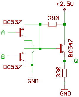
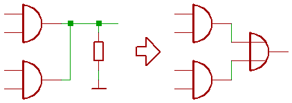
With BC847\BC857 low frequency transistors, a two input AND gate only has 74F speed.
If anybody knows the speed rating when using something like BFR93A and BFT92 transistors instead, please post it here.

Edit2:
Dang !
PNP RF transistors suddenly are tagged "obsolete" at the distributors.
//Makes me wonder, if them distributors are reading my forum postings. ;)

;---

Would like to mention, that from the 6502 cycle diagrams it looks possible to do the flag evaluation for an ALU result in the next machine cycle,
but this could complicate having cycle exact conditional branches.

Another idea is having the microcode in SRAM or FERAM instead of EPROM.
Fast FERAM might be a bit exotic, and SRAM requires that the microcode is copied from ROM to RAM after power on.
An the other hand, being able to load custom microcode into the CPU during runtime might be an interesting option...
when considering line drawing or fast math routines.

That's all so far.


Last edited by ttlworks on Thu Aug 01, 2019 12:47 pm, edited 2 times in total.

Top
 Profile  
Reply with quote  
PostPosted: Sat Apr 13, 2019 2:09 pm 
Offline
User avatar

Joined: Thu Dec 11, 2008 1:28 pm
Posts: 10760
Location: England
Interesting ideas! Especially the Cray-like techniques for reducing overheads.

For me, as soon as it looks difficult to run the whole system at some speed, it makes sense to look at decoupling. Each clock cycle of the CPU can be a different length, depending on what is being accessed. Even a small cache could be helpful, because many accesses are sequential. In the case of 6502, you might get a gain from specific caching or write-buffering of page zero and page one.

Performance modelling is the answer, I think: not to build all possible systems, but to model them in software.


Top
 Profile  
Reply with quote  
PostPosted: Sat Apr 13, 2019 3:04 pm 
Offline
User avatar

Joined: Wed Mar 01, 2017 8:54 pm
Posts: 660
Location: North-Germany
Dieter,

I think it would be helpful to say something about the design "frame" - that is what is the goal and what not. You are thinking about a 6502 (NMOS? or perhaps 6510?) CPU running cycle-correct(?) at 40/50/more MHz (so far OK) that could run(?) within(?) a C64 ??? I am by no means a C64 child - to me these "breadboxes" have had a surprising success and only through some posts within this forum I gain some knowledge about this machine - e.g. the interesting SID within...

Then it appears to me you are somehow referencing the TTL-CPU Drass has built. Starting a new thread is a good point to summarize and simplify (but please remember Albert E.) what has been done over there. Again I am by no means an expert to the Drass-TTL-CPU - references to the unknown aren't helpful.

So please explain what the aim is and what for the references to the C64 are (a sort of proof of concept perhaps?). As far as i know there are FPGA based 65xx emulations running faster than 100 MHz. Doing s.th. similar with discrete logic would be a challenge - s.th. I know you are able to face. I would like to assist a little - if possible.

Cheers,
Arne


Top
 Profile  
Reply with quote  
PostPosted: Sat Apr 13, 2019 11:26 pm 
Offline
User avatar

Joined: Sun Oct 18, 2015 11:02 pm
Posts: 428
Location: Toronto, ON
Nice idea to get this discussion started Dieter. Love that 3D construction! :)

I’ve had a chance to refine some thinking on this, and I think it just might be possible for the TTL CPU (Rev B) to run at close to 50MHz. I know, kinda crazy! :shock: I’ll post more extensively about this on the original build thread later, but below is a brief summary for now. (I’ll try to keep the discussion fairly generic here). There are three key concepts:

The first is to eliminate decoding and setup overhead at the start of each cycle. The current implementation spends up to 19ns on strictly preparatory tasks (microcode decode, register select, register enable). This seemed quite reasonable last go-around, but in fact it represents nearly 40% of the cycle at 20MHz! The new idea is simple: complete all setup tasks ahead of time in the prior cycle. With that done, the setup delay is eliminated entirely, and performance would improve dramatically! There are complications, of course, but it sure seems feasible. (The key is registered ALU inputs and a separate DECODE phase. More on that later).

The second key concept is really a consequence of the first. In preparing ALU inputs ahead of time, we can also invert the B-Input of subtract operations in the prior cycle. By doing so, we can eliminate the XOR gates that typically sit in front of the adders in the ALU itself. That might not seem like much, but at these speeds, every gate counts!

The final concept is that the flags can indeed be set in the cycle following the ALU operation. The trick to maintaining cycle accuracy is to do it in a separate pipeline stage which completes in a half cycle (a “WRITE_FLAGS” stage). By arranging things carefully, it’s possible to interrogate the flags in the second half-cycle of a subsequent branch operation, and it all ends well. It’s certainly tight, but I think the timing works.

Based on an initial analysis, the three mods above reduce the critical path of the TTL CPU to just 21ns! (typical tpd). With a little coaxing, and some luck, we just might get to a 50MHz max clock-rate! :D

Now, at these speeds, we will definitely need to use RAM for microcode storage. That does imply bootstrapping on powerup, but standard SRAMs can easily meet the timing requirement once loaded.

Then there is the issue of construction — I’d like to take some measurements across the existing boards with a 50MHz clock just to see how bad things get. Who knows, maybe we can get away with the current trace length? Anyway, there’s lots of work still to do to validate, and the ideas above may improve results even further. Very exciting. As always, any and all input welcome!

Regarding the C64, I’ve been thinking about an adapter that will let the TTL CPU run at high clock-rates even while connected to a C64. It would be a fairly simple affair, with shadow RAM and appropriate wait-stating. I’d like to include a GAL address decoder too, so it can be programmed to work with any 6502 or 6510 vintage system. It would be very interesting to look at ideas to improve performance. (like caching, write-buffers, etc. ... shadow RAM seems a simple way to deal with zero and one page, but not screen RAM — that would really benefit from a write-buffer!)

Anyways, yeah, how cool would it be to have a 50MHz retro computer with a totally retro TTL CPU to boot! :)

Cheers,
Drass

_________________
C74-6502 Website: https://c74project.com


Top
 Profile  
Reply with quote  
PostPosted: Sun Apr 14, 2019 2:24 am 
Offline
User avatar

Joined: Wed Mar 01, 2017 8:54 pm
Posts: 660
Location: North-Germany
Thank you Drass for clarification. It will be challenging, for sure. :)


Top
 Profile  
Reply with quote  
PostPosted: Sun Apr 14, 2019 3:10 pm 
Offline
User avatar

Joined: Sun Oct 18, 2015 11:02 pm
Posts: 428
Location: Toronto, ON
GaBuZoMeu wrote:
Thank you Drass for clarification. It will be challenging, for sure. :)
I agree ... the optimizations above are theoretical at this stage, and there’s likely to be more than one fly in the ointment as we go.

Still, it’s very motivating. I find the idea of a multi-stage pipeline in a 6502 particularly exciting. My (probably very naive) understanding is that pipelining is predicated on a regular instruction-set, something that the 6502 lacks. But, the microcode *is* regular. Indeed, the CPU does not execute opcodes at all, but rather runs microcode, and how that happens is entirely under our control. So, perhaps pipelining is possible after all.

The additional challenge is cycle-accuracy. If you simply insert new pipeline stages, throughput increases, but so do cycles-per-instruction. That’s not something we can afford here. Thankfully, it is possible to add new processing phases without corresponding additional cycles. In the case of a DECODE phase, it can occur along with FETCH, simply because FETCH retrieves microcode, and DECODE decodes the opcode, and one does not depend on the other. Similarly, we can tuck the WRITE_FLAGS phase into the first half of the EXECUTE cycle of a Branch instruction, without penalty.

The result is a neat [FETCH — DECODE — EXECUTE — WRITE_FLAGS] pipeline, which runs very regular microcode, to implement the very irregular 6502 ISA, in a cycle-accurate fashion, with a very short critical path ... at least that’s the theory. :)

_________________
C74-6502 Website: https://c74project.com


Top
 Profile  
Reply with quote  
PostPosted: Tue Apr 16, 2019 4:48 pm 
Offline
User avatar

Joined: Fri Nov 09, 2012 5:54 pm
Posts: 1387
GaBuZoMeu wrote:
So please explain what the aim is and what for the references to the C64 are

Currently, we have a 6502 compatible TTL CPU which makes 20MHz.
The aim is just to make up an odd collection of ideas (whether they make sense or not) for breaking that 20MHz "sonic barrier".
If somebody starts a 6502 TTL CPU related project later (whether it's team C74 or not), this collection might be helpful for that project.

C64 just seems to be "the king class" when it comes to 6502 compatibility testing, because the coders had pulled a lot of odd tricks
over the years for squeezing as much speed and functionality out of the C64 as possible/impossible.

GaBuZoMeu wrote:
I would like to assist a little - if possible.

Thanks. :)
If you happen to have any odd ideas for building a faster CPU, just post them here.


Top
 Profile  
Reply with quote  
PostPosted: Tue Apr 16, 2019 4:52 pm 
Offline
User avatar

Joined: Fri Nov 09, 2012 5:54 pm
Posts: 1387
Drass wrote:
I’ve had a chance to refine some thinking on this, and I think it just might be possible for the TTL CPU (Rev B) to run at close to 50MHz. I know, kinda crazy! :shock: I’ll post more extensively about this on the original build thread later,

The original build thread went quite long over the years, and it became hard to find the one or other old post in there.
Maybe it would be better to have the "odd\speculative stuff" in this thread, while the old build thread focuses on building/completing the old hardware. ;)

BTW: from what I have seen:
At 1MHz, doing something wrong isn't easy for the experienced hobby tinkerer.
At 4MHz, you have to consider only a few things.
At 20MHz, you have to consider a lot of things.
At 33MHz, trace length becomes a topic (that's when I had to build a S5935 based PCI card at work).
At 66MHz, trace impedance and line termination might become a topic (another fun project at work had been building a 74F163 based pulse width modulator clocked with 80MHz).

Drass wrote:
a regular instruction-set, something that the 6502 lacks.

Now that's a long story.
When taking a look at the MT15 instruction set, where instruction words have 16 Bit, this gives 65536 possible Opcodes.
In the time frame when the 6502 was invented, RAM did cost an arm and a leg, so it made sense to compact/limit the instruction word to 8 Bit...
at the cost of a more complicated instruction decoding inside the CPU.

So one could start with making a list of the 65536 possible MT15 opcodes,
then scratch the opcodes from the list which obviously don't make sense,
then analyze code for opcodes which are not used often and scratch them from the list, too...
And then to "fold" what is left from the list into a smaller instruction word
(a game somewhere between Tetris and Origami, with a little tad of Sudoku.)
Of course, trying to "unfold" the 6502 instruction set won't be fun, and the UFO compatibility would be going to be a big problem.

IIRC the 68000 had used three PLAs for instruction decoding, which generated a 10 Bit microcode address.


Hmm...would it make sense to start a discussion about compacting the microcode ?
Drass, how many percent of the microcode ROMs is filled with NOPs ?
(Please write a little bit of C code which counts the empty slots in th microcode ROM binaries or such...)


Top
 Profile  
Reply with quote  
PostPosted: Tue Apr 16, 2019 11:33 pm 
Offline
User avatar

Joined: Wed Mar 01, 2017 8:54 pm
Posts: 660
Location: North-Germany
Thanks, Dieter, for explaining. I assume the compatibility test with the C64 were not executed at max speed ;)

Ideas - little to nothing. Need to have a look at the opcode map and the cycle behavior when an interrupt appears. But when things appear to require sequential operation I try to imagine what happens if all possible second steps were provided (done) in parallel and when the preceding step is done just selected. Would this be beneficial (regardless of the massive hardware needed)?


Top
 Profile  
Reply with quote  
PostPosted: Wed Apr 17, 2019 10:18 pm 
Offline
User avatar

Joined: Sun Oct 18, 2015 11:02 pm
Posts: 428
Location: Toronto, ON
ttlworks wrote:
Maybe it would be better to have the "odd\speculative stuff" in this thread ... ;)
Sure. Let’s do it here. I wanted to illustrate a little more how the new pipeline will work. This discussion is specific to the C74-6502, but the concepts apply generally.

The previous pipeline had just FETCH and EXECUTE phases. This new pipeline extends that concept with DECODE and WRITE_FLAGS. At any one time, different micro-instructions are in process in the various pipeline stages, with the result of every stage being latched for use by the next stage, as follows:

  • FETCH — microcode is fetched and clocked into the Micro Instruction Register (MIR)
  • DECODE — the opcode is decoded and input data clocked into Input registers (ALUA, ALUB, ALUC, MAR)
  • EXECUTE — performs ALU operation and/or memory read/write. The ALU result is latched at the output of the ALU. Memory data is latched into the ALU B register.
  • WRITE_FLAGS — (a 1/2 cycle stage) Flags evaluated based on the ALU result and clocked into the P-Register

In the old pipeline, FETCH retrieves microcode in one cycle, and EXECUTE implements everything else in the next. But in fact, EXECUTE performs several distinct operations which can be parallelized further. It begins by decoding control signals, and selecting and enabling specific input registers. That takes 13ns to complete. We also take an additional 6ns to invert the B input of the ALU for SBC operations. Let’s call the activity to this point the DECODE phase. It takes 19ns in total. Then we have the ALU itself at 21ns (and/or memory read/write). Finally, after the ALU operation is complete, we take an additional 10ns to evaluate and set the flags.

So, EXECUTE actually breaks down into DECODE (19ns), EXECUTE (21ns) and WRITE_FLAGS (10ns). The new pipeline simply pulls the DECODE processing into the prior cycle and pushes WRITE_FLAGS into the next, leaving EXECUTE as a 21ns critical path.

DECODE’s function is to decode the opcode and pre-load the input registers (ALUA, ALUB, ALUC for the ALU and the Memory Address Register (MAR) for memory reads and writes). The opcode pretty much tells us all we need to know to set things up. The only potential glitch is when we don’t yet have a valid opcode. Thankfully, FetchOpcode is reliably followed by a FetchOperand, so there is no mystery as to what we need to do. (Single cycle NOPs are an exception, of course, but they are easily handled as such).

Ok, with the input registers pre-loaded by DECODE, both the ALU and memory can begin work immediately upon the clock transition. The setup overhead is eliminated. Meanwhile, flag evaluation can be done in half a cycle, so it’s safe to push that processing to the following cycle. A branch which may follow can use of the flags in the second half of the cycle, and the flags overhead is similarly eliminated.

The implementation for this is surprisingly straight forward. Effectively, we take the existing microcode and split it into its DECODE and EXECUTE components. The DECODE microcode includes any control signals that manage a given operation’s inputs, while the EXECUTE microcode includes signals that configure the datapath and clock the result into destination registers. We then arrange for the DECODE microcode to go directly to the datapath, while the EXECUTE microcode is latched into the MIR and used in the next cycle. And with that simple change, we get the correct action: DECODE pre-loads the registers in the prior cycle, EXECUTE performs the operation and latches the result in the cycle that follows.

It turns out that the datapath can also be readily adapted to this new scheme. We have to add an ALUA input register, but we already have an ALUB register, and the Internal Carry can be repurposed as ALUC as well. Similarly, the DPH and DPL registers can be repurposed to be the MAR. As an added bonus, the DECODE microcode can replace all the complicated gate logic we currently use in the microcode pipeline, and we can now dispense with it. In fact, the new design is likely to be much more streamlined and faster at the same time.

The next step is to modify the Logisim model and validate. I’ll report back once that’s done. In the meantime, I’ll try to post up some signal path details later so we can see how the new pipeline impacts the critical path.

Quote:
Drass, how many percent of the microcode ROMs is filled with NOPs ?
We can estimate: 256 opcodes * 4 cycles per opcode on average * 3 variants (6502, 65C02, K24) * 2 alternate versions for each (with and without the K24 special opcodes) = 6k. There is a lot of empty space in those ROMs.

_________________
C74-6502 Website: https://c74project.com


Top
 Profile  
Reply with quote  
PostPosted: Thu Apr 18, 2019 5:21 pm 
Offline
User avatar

Joined: Fri Nov 09, 2012 5:54 pm
Posts: 1387
GaBuZoMeu wrote:
I assume the compatibility test with the C64 were not executed at max speed ;)

C64 compatibility testing was done at ca. 1MHz (C64 speed).
IIRC the use of the UFOs (instructions UnFOrseen by the designers) puts a 14MHz speed limit to the CPU.

GaBuZoMeu wrote:
Ideas - little to nothing.

No problem:
Distributing the control and clock signals and arranging the function blocks in 3D to have shorter trace lengths
also is a big construction site, any ideas\suggestions on this ?

GaBuZoMeu wrote:
But when things appear to require sequential operation I try to imagine what happens if all possible second steps were provided (done) in parallel and when the preceding step is done just selected.

Now that's going to be a big can of worms and a lot of text.
When making the microcode memory 8 times as wide, one could not just fetch the microcode for the next machine cycle,
but for the next 1..8 machine cycles for putting the microcode of a complete instruction into a control pipeline.
But that would be going to be a lot of memory chips, and for making efficient use of such a mechanism
you probably would want to prefetch the next instructions at some point.
But then you need to check how many Bytes an instruction has, and to detect possible changes in program flow
(JMP, JSR, conditional branches etc.) for dropping/discarding control pipeline contents in the right moment.


Top
 Profile  
Reply with quote  
PostPosted: Thu Apr 18, 2019 5:25 pm 
Offline
User avatar

Joined: Fri Nov 09, 2012 5:54 pm
Posts: 1387
Drass: nice going.

The TTL CPU we have now uses vertical microcode.
Using horizontal microcode instead would shave off a few more nanoseconds.

Considering that EXECUTE now is the slowest step, spending thoughts on building a better/faster carry chain makes sense indeed.

Drass wrote:
We can estimate: 256 opcodes * 4 cycles per opcode on average * 3 variants (6502, 65C02, K24) * 2 alternate versions for each (with and without the K24 special opcodes) = 6k. There is a lot of empty space in those ROMs.

We seem to be using 32kB microcode ROMs, so ca. 81% of these 32kB are nothing but empty space, thanks.

In the good old times (1980), big memory chips were slow, and small memory chips were fast.
Nowaday (2019), the situation seems to be reversed somehow... ;)

Tricks for shrinking the microde to the smallest size possible won't be useful now...
But just in case there might be very fast but small memory chips somewhere in the future,
I feel a need to add my two cents on it. (Drass, I'm not expecting you to read this in detail.)

;---

One way to go for compacting the microcode would be the AM2910 approach.
The idea is to have a fast lookup table which generates the start address for the microcode sequence for a given instruction.
Downside is, that you would need to have a microcode address counter feeding _all_ of the address lines of the microcode ROMs.
AM2910 also had featured calls\subroutines in the microcode, for instance with a one level deep hardware stack
one could have the sequence for nearly all of the addressing modes of the instructions as subroutines,
this will compact the microcode even further.

Image

When following this path, maybe one could stuff the whole K24 functionality into less than 2k of microcode memory.

;---

A different trick would be using something like two lookup tables and a (for instance) 3 Bit state machine.

In some old SciFi literature, there are two types of spacecrafts:
Jumpships, which only are designed for jumping from one solar system to the next, faster than light, but they are not meant to enter a solar system.
Dropships, which are designed to enter a solar system and to land on a planet, but they are not meant to even getting close to light speed.

Usually, a jumpship carries some dropships as the payload, and I think that the basic concept for using the two lookup tables is somewhat similar:


The first lookup table interacts with the state machine counter (which could be just a 74273),
and does the sequence for the addressing modes, generating the related control signals to the mill.
For NMOS 6502, we could estimate a 256*8=2k size for the first lookup table.

When the ALU handles data instead of doing address calculation, the first lookup table tells the second lookup table
"everything is in place, now do the job and process the data, take over some of the control signals for ALU, flags
and some registers for the next machine cycle."
The second lookup table would have 256 entries only.

Hmm... there might be some logic design tricks for further compacting these two lookup tables,
but using them probably would reduce the speed of the design, sorry.


Top
 Profile  
Reply with quote  
PostPosted: Fri Apr 19, 2019 6:26 am 
Offline
User avatar

Joined: Sun Oct 18, 2015 11:02 pm
Posts: 428
Location: Toronto, ON
ttlworks wrote:
The TTL CPU we have now uses vertical microcode.
Using horizontal microcode instead would shave off a few more nanoseconds.
Resolving the microcode is no longer on the critical path with the new pipeline. For both DECODE and EXECUTE microcode, the control signals are needed only at the end of their respective cycles, and the WRITE_FLAGS control signals are propagated from the EXECUTE cycle. We *should* have lots of time, therefore, to deal with vertical microcode — if I can manage encode it appropriately, that is.

Quote:
Considering that EXECUTE now is the slowest step, spending thoughts on building a better/faster carry chain makes sense indeed.
Yes, definitely. There are a couple of paths that land at 21MHz, including the Adders. It would be great if we could improve those. The current concept is to use the Carry Skip Adder you suggested:
Code:
ALUA       74AC574       6.0   CLK to Q for input register
ADDER      74AC283      10.6   Low-byte Adder
SKIP.ADR   74AC257      4.5    High-byte Skip Adder
ADR.OUT    74CBT3245    0.25   ALU output select
The MT15 carry chain looks great, and it’s much faster for 16 bits. Does it help with an 8-bit ALU?

Quote:
We seem to be using 32kB microcode ROMs, so ca. 81% of these 32kB are nothing but empty space
I know. Up to 16 bytes per opcode are reserved in the ROMs, and there was no real attempt made to optimize this. :oops:

_________________
C74-6502 Website: https://c74project.com


Top
 Profile  
Reply with quote  
PostPosted: Sat Apr 20, 2019 12:39 pm 
Offline

Joined: Sat Aug 19, 2017 1:42 pm
Posts: 35
Location: near Karlsruhe, West-Germany
Drass wrote:
Anyways, yeah, how cool would it be to have a 50MHz retro computer with a totally retro TTL CPU to boot! :)

In 1987 I bought an accelerator board for my Apple IIe. The source:

Image

My card runs the CMOS instruction set at 12,5MHz and has 144kB of fast RAM because it emulates an Apple IIe with 128kB DRAM on motherboard. The board was really two boards :-) One in the slot, the other as piggyback onto the first.

This one is the first:

Image

The piggyback:

Image

The two creators (Schaetzle & Bsteh) developped this CPU primarily for their chess computers, or for acceleration existing chess computers.
https://www.schach-computer.info/wiki/i ... p/TurboKit
http://chess-computer.blogspot.com/2015 ... 8-mhz.html
I've heard that one board exceeded 20MHz.

In late 1987 my Apple IIe ran at 12,5MHz, the RAM disks ran with 333kB/sec (read) and 500kB/sec (write). Now I'm preparing to resume this Apple IIe. I bought a new power supply because this cards consumes 5A @5V and I don't trust the old switching power supply. The original power supply can just deliver 2,5A for the whole machine. New fans will be installed too. And I wrote accelerated drivers for the RAM disks (AE RAMFactor): 800kB/sec (write) and 500kB/sec (read) :-)

Image

If anybody knows another owner of this Apple II accelerator board please notify me. I have never seen another board from Schaetzle & Bsteh. I just know that my board was the first built to emulate an Apple IIe instead of a II.

Regards,
Ralf


Top
 Profile  
Reply with quote  
PostPosted: Sun Apr 21, 2019 11:29 am 
Offline
User avatar

Joined: Sun Oct 18, 2015 11:02 pm
Posts: 428
Location: Toronto, ON
It's great to see the TK20 boards. Thank you for posting these pics! I was not aware ones existed for the Apple IIe, and you say yours was the first. Very cool.

Interesting to note 74F family ICs, six 74F181s no less. and multiple PALs. Wow. Lots of "iron" on those boards. :)

Cheers.

_________________
C74-6502 Website: https://c74project.com


Top
 Profile  
Reply with quote  
Display posts from previous:  Sort by  
Post new topic Reply to topic  [ 149 posts ]  Go to page 1, 2, 3, 4, 5 ... 10  Next

All times are UTC


Who is online

Users browsing this forum: No registered users and 3 guests


You cannot post new topics in this forum
You cannot reply to topics in this forum
You cannot edit your posts in this forum
You cannot delete your posts in this forum
You cannot post attachments in this forum

Search for:
Jump to: