6502.org Forum  Projects  Code  Documents  Tools  Forum
It is currently Sat Apr 27, 2024 9:38 pm

All times are UTC


Post new topic Reply to topic  [ 189 posts ]  Go to page 1, 2, 3, 4, 5 ... 13  Next
Author Message
PostPosted: Sun Mar 31, 2019 8:39 pm 
Offline

Joined: Fri Jan 25, 2019 2:29 pm
Posts: 191
Location: Madrid, Spain
Hi all!

Even though I've been working on this idea for about 8 months already, I've finally reached a point where I can be pretty confident on the final result. So I've finally decided on opening a thread to share my progress, an hopefully get some good tips from all the clever minds in the forum.

The idea behind the project is, as you have probably guessed from the title, is to build a MOS6526 replica, out of 74xx ICs. The main motivation, besides having fun and learn something new, is to be able just replace the CIAs in Commodore computers (Of course, with quite a bulky gizmo!). Main goal, making it work up to 2MHz. Beyond that.. well, as far as I can reach!

Just a little background on myself. I'm no expert in electronics, but in computers. I have some solid knowledge on digital circuits but only on the theoretical part of it. The only time I've done some tinkering with real chips in my life, was back in college, and nothing outside a breadboard.

What have I accomplished that makes me feel confident in my success chances? Before going all in in recreating a chip I didn't even understand, I've focused on building something much simpler. I've made a single byte register, with some address decoding, and I've attached it to my good old C64 into the expansion port... and yes! It didn't go up into smoke, and it did work flawlessly. I could read a byte, store a byte.


This means I've understood the bus timings, and I can now build a 65xx bus compatible peripheral. Yay!

Now the work on the 6526 begins. I already have the schematics for the DDRs, PORTs, and CREGs, and the TIMERs are like 50% done. I need to make my schematics a bit more clear before sharing them... but I'll post them shortly.

I'm pretty much a noob in many areas so... expect some weird solutions to pop up. Any corrections or advice will be welcome!

Stay tuned.

12/09/2021: After a 10 month halt on the project, I've been gaining momentum again with it for the last 3-4 weeks, and hopefully I can get some results from this. The project is now going through a reboot, moving away from EAGLE CAD and into KiCAD. I've decided to take down my old repository, and my new one is now 100% public.

GitHub repos:
SBC6526 https://github.com/dmolinagarcia/SBC6526
LOGISIM6526 https://github.com/dmolinagarcia/LOGISIM6526
74HCT6526 https://github.com/dmolinagarcia/74HCT6526

Of course... everything is untested, experimental, and may catch fire if anyone tries to build their own.


Last edited by daniMolina on Sun Sep 12, 2021 8:08 pm, edited 5 times in total.

Top
 Profile  
Reply with quote  
PostPosted: Thu Apr 04, 2019 5:56 pm 
Offline
User avatar

Joined: Fri Nov 09, 2012 5:54 pm
Posts: 1392
Would be nice, if you could tell us how many experience with hardware tinkering you already have,
to avoid digging too deep into some boring basics.;)

Now for some more boring basics.

Attachment:
edge_boring_basics.png
edge_boring_basics.png [ 54.86 KiB | Viewed 12635 times ]


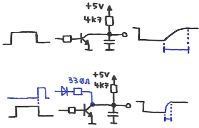
"Open collector" means, the driver only is able to switch the output pin to GND.
For 74LS, it's something like a bipolar NPN transistor as in the picture above.
For 74HC(T)\AC(T), it's a FET instead, but the concept remains the same.

The 74125\74126 buffer has a push/pull output, means there is (at least) another transistor
for sending current from VCC into the output too...
but when connecting the input of the buffer to GND and just tinkering with the output enable,
the buffer just works like a 7405 or such.

(There are chips like 7405 with an open collector output,
but sometimes they are not available as AC(T), and 74125\74126 gives a nicer PCB layout.
That's why I had used 74125 and 74126 in my experiments).

But back on topic:
To have a logic high level at an open collector output in case the output isn't switched to GND
by the output transistor, we also need a pullup resistor (4k7 in the picture),
pulling the output to a logic HIGH level.

And that's where the problem starts if you try aiming for speed:
Because of the output resistor, the falling edge of the output signal will be fast,
but the rising edge of the output signal is slowed down by the value of the pullup resistor
and the capacitive load attached to the output pin (as resistor plus capacitor are forming
sort of a "low pass filter").

There is a limit for making the pullup resistor smaller:
Output transistors of a NMOS 6522 or 6526 probably can't pull much current to GND,
so the voltage at the output won't reach logic low level if too much current goes through the pullup resistor.

(Imagine a scenario, in which you have a C64 with a TTL 6526, with a fast loader parallel cable
which goes from that 6526 to an old NMOS 6522 inside the 1541 floppy drive).

An alternative to having a smaller pullup resistor when trying to improve rise time of the output signal
would be to "inject" some current for a short moment, let's say half a PHI2 cycle
(the blue diode and the blue resistor in the picture above).
Haven't tested this idea, of course, so I can't tell how old NMOS chips would like this approach.

;---

But back on the capacitive load in the picture.

Attachment:
probehead.png
probehead.png [ 85.25 KiB | Viewed 12635 times ]


When attaching something like a 1:1 logic probe to the open collector output,
you have the capacitance of the scope plus the capacitance of the cable.
(I'm simplifying things a bit here).

When attaching some circuitry to the open collector output,
you have the capacitance of the PCB traces to GND (and/or between the traces),
plus the capacitance of the IC input pins which are tied to that output.

You don't need to know the boring basics about the innards of scopes and TTL chips, of course.

;---

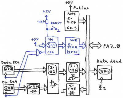
Now for a block diagram for an 8 Bit open collector output port:

Attachment:
port_opencollector.png
port_opencollector.png [ 225.07 KiB | Viewed 12635 times ]


Be warned: That blue marked speedup stuff only is hypothetical and untested.

Remembering my TTL 6522 experiments, there is a latch for reading what's on the port,
and it samples at the rising edge of PHI2...
and I think that the designers intentionally had built it this way for better noise immunity.

About that little box labeled TVS: that's just protection diodes for clobbering down transients.
When trying to drive long lines at higher speeds, adding such diodes might be a good idea.

Too much text, loo little time, if you have some questions please feel free to ask.


Top
 Profile  
Reply with quote  
PostPosted: Thu Apr 04, 2019 8:12 pm 
Offline

Joined: Fri Jan 25, 2019 2:29 pm
Posts: 191
Location: Madrid, Spain
ttlworks wrote:
Would be nice, if you could tell us how many experience with hardware tinkering you already have, to avoid digging too deep into some boring basics.;)


Basically, none. Some 4 months of electronics lessons back in college, but this was 20 years ago, and I barely passed it :). I made a career in computers, focused on DB administration... so that won't be useful here.

I did great in digital electronics though. The biggest obstacle I'm facing with this project is my lack of "real world" knowledge though. It took me just a couple of weeks to complete my the first design of the DDR, PORT, CReg and TIMERs of the 6526, along with all the needed glue logic, and sure, they all work flawlessly... if there were no propagation delays, impedance, etc. This is the main reason I'm just aiming for 1 Mhz for now. I expect to learn a few things along the way so I can push my design faster afterward.

Having no previous experience in something like this, it's very likely I'm finding weird and suboptimal solutions. Again, first, make it work, then make it fast, then make it beautiful.

Let me show you what've done until now.

I plan to split the design in 4 separate 10cmx10cm 2-layer boards. Cutting cost is the main factor here, as this are the biggest boards I can get manufactured at the lowest cost. Not ideal, but good enough for 1 Mhz.

Attachment:
block.png
block.png [ 6.1 KiB | Viewed 12617 times ]


Register decoder and selector. Two 138's (enabled by /CS) to select one of the 16 internal registers. Together with /RES and R/W to enable the write or read portion of the register.
Attachment:
001_RWN_truthTable.PNG
001_RWN_truthTable.PNG [ 29.77 KiB | Viewed 12617 times ]


How did I come to this? Out of the 16 registers, 12 of them are set to all 0's on reset, 4 of them to all 1's. I did find some 8-bit registers with a Reset pin but couldn't find any with a ¿SET? pin. Instead, I gated the data bus together with the reset signal so I have two read internal buses. Whenever reset is high, both buses reflect the contents of the data bus. When reset goes low, one of them reads all 0's, the other read all 1's. My glue logic signals all internal registers to latch the value on the data bus on reset. Atypical? Maybe. But so far... tested and working as expected :)

Attachment:
ddr_bw.png
ddr_bw.png [ 14.33 KiB | Viewed 12617 times ]

Attachment:
port_bw.png
port_bw.png [ 26.67 KiB | Viewed 12617 times ]


DDRs are pretty simple, 8 bit register, with the value of the register forwarded to the PORTs to select the direction of each pin.
PORTs aren't too complicated either... however, I have some serious doubts with them. According to the original datasheet, both PORTs are "open collector outputs, with both active and passive pullups". The schematic I've posted was my final design so far... however the ideas posted by ttlworks have turned my world upside down! (Well, my PORTs at least)

DDRB is exactly the same as DDRA, while PORTB has some additional bits. As PB6 and PB7 can act as timer outputs, a couple of 2-1 selectors coupled with 2 control bits from the CREGs accomplish this.

So far, all the glue logic, and both DDRs and PORTs fit nicely in Board 0. Next, I'm going to build a prototype of the ports. I have two spare real 6526 so I'll connect them to my prototype to make them talk to each other. Hopefully I'll be able to get some insights on how the outputs are configured.

I probably should mention... I have no measurement equipment. No oscilloscope, no logic analyzer... just an extremely cheap multimeter that's falling apart! So right now I'm a bit limited at what I can do. I plan to buy them in the near future though.


Top
 Profile  
Reply with quote  
PostPosted: Thu Apr 04, 2019 8:21 pm 
Offline
User avatar

Joined: Thu Dec 11, 2008 1:28 pm
Posts: 10793
Location: England
daniMolina wrote:
... first, make it work, then make it fast, then make it beautiful.

Nice one!

Quote:
I probably should mention... I have no measurement equipment. No oscilloscope, no logic analyzer... just an extremely cheap multimeter that's falling apart! So right now I'm a bit limited at what I can do. I plan to buy them in the near future though.

A logic probe is an idea. And a multimeter with a frequency counter. And a logic analyser these days can be a very cheap piece of kit which connects to a PC over USB.


Top
 Profile  
Reply with quote  
PostPosted: Thu Apr 04, 2019 11:00 pm 
Online
User avatar

Joined: Fri Aug 30, 2002 1:09 am
Posts: 8428
Location: Southern California
BigEd wrote:
And a multimeter with a frequency counter.

And to extend the frequency range, you can use an inexpensive 74-family counter or divider IC, since DMMs' frequency-counter function usually does not go up very high, and even if it did, the long, plain, single-wire leads are not suitable for high frequencies. My DMM goes to 200kHz; so a pair of cascaded divide-by-ten ICs would get me to 20MHz. It looks like cascading the two sections of a '390 should do the job. (I also have an 8-digit, half-GHz counter on the workbench, but I realize few people do.)

_________________
http://WilsonMinesCo.com/ lots of 6502 resources
The "second front page" is http://wilsonminesco.com/links.html .
What's an additional VIA among friends, anyhow?


Top
 Profile  
Reply with quote  
PostPosted: Sat Apr 06, 2019 11:57 am 
Offline
User avatar

Joined: Fri Nov 09, 2012 5:54 pm
Posts: 1392
daniMolina wrote:
I have no measurement equipment. No oscilloscope, no logic analyzer...

At some point you would need to buy an oscilloscope...
But when trying to build something like a 4 MHz TTL 6526, I think that a used 60MHz analog scope from the "flea market" might do.

Say... it looks like you have two nearly identical I\O ports and two nearly identical 16 Bit timers in the design.
If you would make schematics and layout for one PCB which contains one I\O port and one 16 Bit timer,
then order/solder two identical PCBs, I think this might save you some time and effort.


Top
 Profile  
Reply with quote  
PostPosted: Thu Apr 18, 2019 5:07 pm 
Offline

Joined: Fri Jan 25, 2019 2:29 pm
Posts: 191
Location: Madrid, Spain
Slowly, but steady, I'm making some progress.

I've got a logic analyzer, and an oscilloscope is on its way home. Hopefully, I'll be able to get some insights on a genuine MOS6526. So far, I've taken some measurements with the logic analyzer, and, even though it's not the fastest (can't do more than 8Mhz) it's giving me something.

PORT outputs fall and rises time is always < 0.125us. (Below the maximum resolution of the analyzer). I also have the timings on the /PC output, that signals a read or write to PORTB, used for handshaking.

Attachment:
R00_port_CIA_TIMING.PNG
R00_port_CIA_TIMING.PNG [ 23.66 KiB | Viewed 12480 times ]


I already had the circuit for the /PC generator, but I got it wrong. As the 6510 seems to do a read just before a write (I guess this also happens with the 6502, and probably the 65816, that's something I need to investigate) it was making my circuit to generate to separate pulses, instead of a 2 cycle, single pulse. Good thing, the new design is simpler, allowing me to save an inverter and to AND gates.

I'm building now a test bench for the ports. When the oscilloscope arrives, I'll check rise and fall times on the outputs of the ports, as well as confirming the /PC pulse is OK. With all that, I think it should be enough to complete DDR and PORTs. I have a preliminary PCB layout with all the decoding logic, and both DDRs and PORTs fitting in a single 10cmx10cm board (The biggest I can get cheaply!)


Top
 Profile  
Reply with quote  
PostPosted: Wed May 01, 2019 4:48 pm 
Offline

Joined: Fri Jan 25, 2019 2:29 pm
Posts: 191
Location: Madrid, Spain
Finally got my hands on an oscilloscope and some spare time to give it a try.

I've compared my build against a real MOS6526, and results are... well. Mixed, at least.

Attachment:
port_bw.png
port_bw.png [ 26.67 KiB | Viewed 12396 times ]


Fall time, from logic 1 to logic 0, are pretty much the same in every case. Rise time, when relying only on the pull up resistor, (Port set as input, with nothing connected) are also very close, and the output voltage match.

However, whenever the port is set to output, this is where the biggest diferences are. As I'm actively pulling up the output with the 126 buffer, my design rises much faster and much higher. I get to 5v, while the MOS6526 stays at ~2.9v. (I have a led with a 1K resistor tied to ground in the output).

Despite the differences, I'm within the specs of the datasheet. Will this be good enough to replace a MOS6526? I have two tests in mind.

1) The circuit I built, only uses 1 data bit to save on wiring.... I'm extending it to 5 bits. Why 5? So I can connect a joystick!
2) Replace CIA#2 in a C64. Having no timers, interrupts, or serial, will mean, basically, no Serial Port or User Port access. The test here is, the two lower bits of PORTA act as address bits 14-15 for the VIC-20. If I can bank switch without the computer panicking... that will be a good sign.

I am still confused (even more, I'd say) with this sentence from the data sheet. "Port A and B have passive pull-up devices as well as active pull-ups". I expected the 6526 to be able to pull higher than what I've seen. Until someone does with the 6526 something similar to visual6502, I'll have to rely on the old trial and error method.

EDIT: Small update. I hooked up a 4 bit port (not 5-bit, as this needed 2 aditional ICs) and I was could use a Joystick on this beauty with no problems at all :)


Top
 Profile  
Reply with quote  
PostPosted: Tue Jul 02, 2019 7:30 pm 
Offline

Joined: Fri Jan 25, 2019 2:29 pm
Posts: 191
Location: Madrid, Spain
Hi all!

Things have been moving quite slowly over the last two months, as I've been quite busy in the real world but, anyway, I've managed to give a little nice push to this project.

I've been able to complete and run enough tests to be pretty confident about everything that goes into what I call, Board 0. This is
- 65xx bus interface
- DDRA and DDRB
- PORTA and PORTB

Once I was satisfied with the design and the PCB layout, I put an order for the pcbs and a bunch of components. Then, even though it took a couple attempts before by soldering skills were, at least, good enough... please let me introduce you to the 74HCT6526-Board0

Attachment:
b0.jpeg
b0.jpeg [ 134.44 KiB | Viewed 12300 times ]


I must say, the soldering is not the prettiest and it even looks a bit awful at some places (Do you notice all the little "spikes"?) but, once it was connected to my battle C64 via the expansion port...

Attachment:
b0_c64.jpeg
b0_c64.jpeg [ 128.72 KiB | Viewed 12300 times ]


Success!! I can write to both DDR, and I've been able to send data from one port to another. I also read two joysticks connected to the ports, and everything worked as expected.

There's just two things that are still not perfect.

Output delay to the ports is much much shorter than on a real MOS6526. I've measured between 125ns and 250ns on a real unit, but mine does it well below 125us. If the datasheet that's around the internet is to be trusted, this is still within specs, as there's no lower limit to it.

Also, the /PC negative pulse that follows a read or write to PORTB happens earlier, although the duration is correct, 1 full cycle. Problem here, I haven't been able to get any real specs on this, so it will need to be tested with some peripherals that used this.

Next step is to replace CIA#2 in a real C64 with this board. PORTA alone should be enough to let the computer boot up properly, and even access the serial port. I still need to grab a working disk drive. This will be for sure a very interesting test!

Beyond this, work on Board1 is, I'd say, 40% completed. Board1 houses both control registers (REG 14 and 15) and both timers (REG 4 through 7).

Cheers!


Top
 Profile  
Reply with quote  
PostPosted: Wed Jul 03, 2019 3:02 pm 
Offline
User avatar

Joined: Sun Oct 18, 2015 11:02 pm
Posts: 428
Location: Toronto, ON
Great progress Dan. A lot has to be right for this much to work. One step closer. :)

It’s going to be very cool to plug into the socket of a 64!

Cheers,
Drass

_________________
C74-6502 Website: https://c74project.com


Top
 Profile  
Reply with quote  
PostPosted: Wed Jul 03, 2019 9:10 pm 
Offline

Joined: Fri Jan 25, 2019 2:29 pm
Posts: 191
Location: Madrid, Spain
Just two words...

Attachment:
IMG_20190703_230334.jpg
IMG_20190703_230334.jpg [ 2.59 MiB | Viewed 12239 times ]


Attachment:
IMG_20190703_230405.jpg
IMG_20190703_230405.jpg [ 3.03 MiB | Viewed 12239 times ]


It works.

I think I'm gonna go celebrate :)

Also, I'm buying a 1541, like, right now!, I have to really test this baby! Although I'm not yet sure if DDR and PORTs are enough for disk drive access... Maybe the Timers are also needed?

Anyway.... I'm really gonna go celebrate!


Top
 Profile  
Reply with quote  
PostPosted: Thu Jul 04, 2019 7:11 am 
Offline
User avatar

Joined: Fri Nov 09, 2012 5:54 pm
Posts: 1392
Congratulations.

IIRC the IEC bus routines in the C64 Kernal don't use timers.

Don't party too hard. :)

Looking forward to see, how the adventure continues.


Top
 Profile  
Reply with quote  
PostPosted: Thu Jul 04, 2019 4:50 pm 
Offline
User avatar

Joined: Sun Oct 18, 2015 11:02 pm
Posts: 428
Location: Toronto, ON
Boy, nothin’ like plugging into a socket on a real C64. :) And that moment when the machine boots — magic!

Congratulations Dani. Great work.

_________________
C74-6502 Website: https://c74project.com


Top
 Profile  
Reply with quote  
PostPosted: Mon Jul 08, 2019 11:09 pm 
Offline

Joined: Fri Jan 25, 2019 2:29 pm
Posts: 191
Location: Madrid, Spain
Well, well... Time to go back to the drawing board I think.

Design for CREG and TIMER is complete and feels functional... However, it's not cycle exact. There is a one or two clock cycle difference regarding timer start, underflow, etc. I feel one or two cycles may be good enough for most cases but... It's driving me nuts at the moment!

I'm following this https://ist.uwaterloo.ca/~schepers/MJK/cia6526.html as reference, as it's the most detailed description of the timers I've been able to find, and, with my current design... Adding all those delays was rapidly increasing my gate count. Still... it doesn't seem complete... it doesn't mention loading the timer from the latch on a write to TxHI when timer's stopped....

Sometimes I wonder if the engineers at MOS/Commodore just put together some pieces of silicon, and afterwards, just write their documentation based on how it behaved, instead of doing it the other way around!

Anyway, by starting from scratch with both units, I think I'm now headed to a clearer, easier and more accurate circuit. We'll see!

Also... I've just bought a 1541 and it should be here in a week or so, so you can expect some exciting news by then.

Cheers!


Top
 Profile  
Reply with quote  
PostPosted: Tue Jul 09, 2019 6:50 am 
Offline
User avatar

Joined: Fri Nov 09, 2012 5:54 pm
Posts: 1392
Timer control logic for the 6522 gave me quite a headache, too.

Would be nice to know what the circuitry in the 6526 silicon looks like,
but I think we won't be able to start dissecting it in 2019.

daniMolina wrote:
Sometimes I wonder if the engineers at MOS/Commodore just put together some pieces of silicon, and afterwards, just write their documentation based on how it behaved, instead of doing it the other way around!

Maybe they sometimes just had not enough time at hands for writing documentation.

Quote from an interview with Bob Yannes (inventor of the SID):
"The funniest thing I remember was getting in a whole bunch of C-64 video games which had been written in Japan.
The Japanese are so obsessed with technical specifications that they had written their code according to a SID spec. sheet (which I had written before SID prototypes even existed).
Needless to say, the specs were not accurate.
Rather than correct the obvious errors in their code, they produced games with out of tune sounds and filter settings that produced only quiet, muffled sound at the output.
As far as they were concerned, it didn't matter that their code sounded all wrong, they had written their code correctly according to the spec. and that was all that mattered!"


If you do hardware design for a living, you are used to datasheets that are not 100% correct and\or leave out some "subtle" details, sorry.

daniMolina wrote:
Anyway, by starting from scratch with both units, I think I'm now headed to a clearer, easier and more accurate circuit. We'll see!

That's the right spirit: better a design with bugs than no design at all. :)
Anyhow, the first revision of new hardware always tends to end up in the trash can, so please don't worry about getting things 100% cycle exact _now_.

BTW: had problems to get hands on down_counters, so for implementing the 6522 timers I just had used 74163 up_counters
and inverted the 74163 data inputs and outputs with some 7404 chips to make them look like down_counters to the CPU.
Inverting bus buffers (74540) would have worked, too.

You got to be creative. :)

Cheers,
Dieter.


Top
 Profile  
Reply with quote  
Display posts from previous:  Sort by  
Post new topic Reply to topic  [ 189 posts ]  Go to page 1, 2, 3, 4, 5 ... 13  Next

All times are UTC


Who is online

Users browsing this forum: No registered users and 38 guests


You cannot post new topics in this forum
You cannot reply to topics in this forum
You cannot edit your posts in this forum
You cannot delete your posts in this forum
You cannot post attachments in this forum

Search for:
Jump to: