6502.org Forum  Projects  Code  Documents  Tools  Forum
It is currently Wed May 08, 2024 4:38 am

All times are UTC


Post new topic Reply to topic  [ 189 posts ]  Go to page Previous  1, 2, 3, 4, 5, 6, 7, 8 ... 13  Next
Author Message
PostPosted: Mon Oct 21, 2019 6:48 am 
Offline
User avatar

Joined: Fri Nov 09, 2012 5:54 pm
Posts: 1393
Nice going.

Quote:
2. START bit gets set to 1 on its own sometimes. Same for both TIMERS.

U3A START flipflop, /PRE input: is it tied to VCC, or is it floating (like in the schematic) ?


Top
 Profile  
Reply with quote  
PostPosted: Tue Oct 22, 2019 7:58 pm 
Offline

Joined: Fri Jan 25, 2019 2:29 pm
Posts: 191
Location: Madrid, Spain
ttlworks wrote:
Nice going.

Quote:
2. START bit gets set to 1 on its own sometimes. Same for both TIMERS.

U3A START flipflop, /PRE input: is it tied to VCC, or is it floating (like in the schematic) ?


Tied to VCC. Here are all the parts involved.

A pair of 138 generate the register enable signal (EN0-EN15) for all registers. They're both qualified by /CS and PHI2, so no register are selected when PHI2 is low.

Attachment:
TIMER_DECODER.png
TIMER_DECODER.png [ 9.34 KiB | Viewed 1713 times ]


The individual register select line is combined with /RES and R/W to generate the WEn and OEn (Write enable and Output Enable, both active low) for each register.

ENABLE_NAND is NAND(R/W,/RES). This is how the original schematic for the register select:


Attachment:
001selectLogic.PNG
001selectLogic.PNG [ 10.66 KiB | Viewed 1687 times ]


The NAND gate labeled inst6 is the ENABLE_NAND. This is common to all registers,

Essentially, when /RES is high, WE equals ENn OR R/W, OE equals ENn OR NOT(R/W)

Attachment:
TIMER_WEOE.png
TIMER_WEOE.png [ 4.62 KiB | Viewed 1713 times ]


And then, this is the DFF storing the START bit

Attachment:
TIMER_START.png
TIMER_START.png [ 5.23 KiB | Viewed 1713 times ]


I am a bit at a loss here... One thing I know, the way I'm generating the clock for the DFF is not entirely correct. If, by any reason, WEn goes low when PHI2 is low, there will be a clock fed into the flipflop, so I'll store whatever is on the bus. However, as both the 138 are disabled when PHI2 is low... WEn shouldn't be enabled at any time!. I may have a bad solder on the second 138.

I haven't looked into this so far as I'm busy with the underflow signal from the 2 chained 688. Most of the time, it works, but sometimes, 1 or 2 counters won't reload their values. I'm almost sure the issue is as follows. As soon as any of the counters reload, the output from the 688 won't be signaling the underflow anymore. I can't see the pulse at 8Mhz with my logic analyzer. At 12Mhz, I get it most of the time, but not always. At 16Mhz my 6$ logic analyzer goes bananas. So I'll need to make this pulse low more time. (but shorter than half a cycle!).


Top
 Profile  
Reply with quote  
PostPosted: Thu Oct 24, 2019 10:29 am 
Offline
User avatar

Joined: Fri Nov 09, 2012 5:54 pm
Posts: 1393
Tried to draw the address decoding a bit differently, then to extract the interesting part of how the START flipflop U3A is written.

Attachment:
dmdecoder1.png
dmdecoder1.png [ 188.54 KiB | Viewed 1683 times ]


I think the reliability problem with the START flipflop could be related to the C64 bus timing.
If the 74377 registers would work well, but the 7474 flipflops with clock gating would not:

The timing in the C64 is a bit difficile (more than in the "average" 6502 system), because the CPU and the VIC-II share the bus.
Because of this, address and data on the bus are not valid at the rising edge of PHI2...
what could give old NMOS 6522 chips some problems,
the usual approach for fixing this was delaying PHI2 with two flipflops clocked by the dot clock or such before sending it into the 6522.
That's one thing you could try.

Another thing you could try is to insert a 74573 chip between C64 and 74HCT6526 for the signals R/W and A3..0,
then to clock it with PHI2, this way those signals at the 74HCT6526 inputs are supposed to stay stable
at the 74HCT6526 inputs after the falling edge of PHI2 when the VIC-II takes over the bus.
//But this won't cover that moment when the CPU takes over the bus again after the rising edge of PHI2.

Anyhow: take an oscilloscope, watch out if there are spikes at the clock input of the START flipflop during PHI2=0.
A cheap logic analyzer probably won't be fast enough for seeing the spikes.
An old/used 60MHz analog oscilloscope with passive 10:1 probes might do.


Top
 Profile  
Reply with quote  
PostPosted: Thu Oct 24, 2019 11:27 am 
Offline
User avatar

Joined: Fri Nov 09, 2012 5:54 pm
Posts: 1393
From the datasheet, the 74HCT193 outputs change after the rising edge of the DN signal.
PHI2 > U14C(7408) > DN0 > U21(74193).DN(pin 4). //Means if the counter is counting, the counter outputs change after the rising edge of PHI2.

The counter outputs are feeding the 74688 comparators U28, U29.
The UNDERFLOW signal generated by the comparators then goes through the logic gates U6D(7408) and U15A(7427) for generating FORCELOAD.
//U10A(7474) flipflop could be accidentally cleared by spikes on FORCELOAD, take care.

But say... the way how FORCELOAD is connected to U12B(7474)... what was your intention when connecting the flipflop like _that_ ?

Attachment:
dmFORCELOAD1.png
dmFORCELOAD1.png [ 8.4 KiB | Viewed 1678 times ]


Top
 Profile  
Reply with quote  
PostPosted: Thu Oct 24, 2019 3:19 pm 
Offline

Joined: Fri Jan 25, 2019 2:29 pm
Posts: 191
Location: Madrid, Spain
As usual, that's plenty of very useful and instructive info. Thanks!

I've got nothing to add on the Start Bit Flipping issue until I grab the scope and find some facts, and stop using guesses. I have a hunch it's happening very close to any of PHI2 edges and some delay is playing tricks on me...

About the FORCELOAD... my first though at that schematic was, "Who did that?". Yep, it doesn't make any sense at all... it's definitely my work, but I can't even remember that. Funny how the mind remembers some things and completely discards others! Must be some early design that I ditched immediately... This is what I have now.

Attachment:
timer_reload.png
timer_reload.png [ 8.12 KiB | Viewed 1663 times ]


Top
 Profile  
Reply with quote  
PostPosted: Thu Oct 24, 2019 3:53 pm 
Offline
User avatar

Joined: Fri Nov 09, 2012 5:54 pm
Posts: 1393
Just trying to help.

The FORCELOAD schematic with the U12B flipflop is on page 2 of this thread, the third picture in this post,
'Jul 20, 2019', and it's the most recent version I had at hand.

But say: from the 74HCT193 datasheet, the /LD input is an asynchronous load.
So you have: counter_outputs > comparators > logic_gates > counter_/LD_input > counter_outputs.

To me, this feels like you might be unintentionally trying to build sort of a ring oscillator. ;)
Oh, and also please take a look at the wikipedia page about propagation delay.


Top
 Profile  
Reply with quote  
PostPosted: Sun Nov 10, 2019 7:27 pm 
Offline

Joined: Fri Jan 25, 2019 2:29 pm
Posts: 191
Location: Madrid, Spain
Hi all!

I'm sorry for this two weeks blackout. After some extremely busy days at work, I didn't find enough spare time for my little big project.

Nevertheless, I've been trying to clean up all the schematics and documentation, as it has started to get a bit messy... In order to limit the mesh of wires and to improve my tests, I've ordered a small PCB to connect two CIAs in the expansion port. My idea is to have a real CIA and my board connected at the same time, so I can code and automate tests. I really needed to tidy up everything.

I'll probably wait until next year until I get my hands dirty again. I'll be around though.

Cheers!


Top
 Profile  
Reply with quote  
PostPosted: Tue Nov 12, 2019 12:50 pm 
Offline
User avatar

Joined: Fri Nov 09, 2012 5:54 pm
Posts: 1393
Sorry to hear about that delay, I know you would _like_ to go on with tinkering.

From my own experience:
When printing out schematics on paper, it's helpful to have a collection of text markers at hand.
Just for marking wires, logic gates and such.

Red: it didn't work.
Blue: it did work indeed. //but why ?
Yellow: it did work, but it could work better.
Green: it might work. //hypothetical bug fix.


Top
 Profile  
Reply with quote  
PostPosted: Thu Dec 26, 2019 3:38 pm 
Offline

Joined: Fri Jan 25, 2019 2:29 pm
Posts: 191
Location: Madrid, Spain
Hi all again!

After a not-so-small break, I'm almost ready to get back to work here. In the meantime, I've managed to bring some order into my chaos.

I've updated the first post in the thread with the most up-to-date schematic I have. I will keep those updated as I work through any issues I may find.

Also, I finally completed a small board that allows me to plug 2 CIA (Either the original ones, or my 74HCT6526) into a C64 without the need to use a mess of wires. Each one of the two CIAs map to the IO1 and IO2 pages in the C64. This will allow me to automate testing, and prevent any issues and headaches caused by bad wiring.

Attachment:
ciacart.jpg
ciacart.jpg [ 182.45 KiB | Viewed 1465 times ]


I've compiled a list of issues too, so no more chasing ghosts! Now it's the time to address onw issue at a time and hopefully, finally be able to move on.

I know eventually chaos will come back, but now I know how to deal with it :)

Cheers!


Top
 Profile  
Reply with quote  
PostPosted: Sat Jan 04, 2020 7:29 pm 
Offline

Joined: Fri Jan 25, 2019 2:29 pm
Posts: 191
Location: Madrid, Spain
I've updated the first post with the current list of issues.

After two full weeks scratching my head with this:

Quote:
START bit gets set to 1 on its own sometimes. Same for both TIMERS.


It turned out to be something soooo obvious that I feel kinda embarrased.

Second '138 decoder (B0 U2) soldering was awful. I think it was one of the firsts I did, but hey, no excuses... It had something like 4-5 completely floating pins. As a result, all enable signals for registers 8-15 were firing all the time. As I just have CREGs there, and all the other bits are loaded only at the falling edge of PHI2, only STARTBIT and, probably, LOAD bit where being set. Reflowing U2 fixed the issue. One less to go :)

Cheers!


Top
 Profile  
Reply with quote  
PostPosted: Sun Jan 26, 2020 4:13 pm 
Offline

Joined: Fri Jan 25, 2019 2:29 pm
Posts: 191
Location: Madrid, Spain
Hi everyone.

Slow but steady progress here. I've spent the weekend further diagnosing ISSUE 5:

5. B12. CNT counts two pulses. OneShot mode counts one additional tick. U10B seems to be updated after the counter has ticked.

It turned out to be not one, but two separate issues.

If you take a look at the "Decrement and Load" portion of the schematic.

download/file.php?id=9002&mode=view

(Shown here is Timer A, Timer B has an additional MUX, as it has more timer input options, but it's irrelevant here)

The oneshot additional tick was solved by clearing the last FF on Underflow, just tying U10B /CLR to FORCELOAD. However, CNT pulses are still counting double, even triple sometimes.

First of all, I've had to add a rising edge detector (made with a flipflop) before U9B. Before this, the timer was ticking every PHI2 cycle if CNT was held high, instead of counting just rising edges. Still, this doesn't fix the double count, although it was something needed.

I've taken some samples with a logic analyzer of the output of the 4 FFs in the chain.
U9B output is A0
U9A output is A1
U10A output is A2
U10B output is DECREMENT.

As U9B goes high for a single cycle whenever there's a rising edge on CNT, you (or at least I) would expect to see a pulse, one cycle wide, going through the pipeline on each PHI2 cycle. And indeed, sometimes I got it

Attachment:
cnt_pulse_ok.PNG
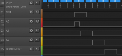
cnt_pulse_ok.PNG [ 21.42 KiB | Viewed 1405 times ]


But, most of the time (over 90% I'd say) this is what I see

Attachment:
cnt_pulse_notok.PNG
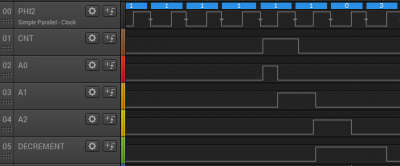
cnt_pulse_notok.PNG [ 20.78 KiB | Viewed 1405 times ]


U10B goes high at the same time as U10A. I haven't been able to find any explanation so far. I've checked the obvious. Verified the soldering, replaced U10 just in case it was bad, tested both TIMERA and TIMERB boards. Same exact result.

The only idea I have right now, is that U10A is getting updated before U10B handles the clock tick, so when the clock reaches U10B, U10A is already high. Considering both FF are on the same IC, both clock pins are separated by a trace no more than 3mm long, so, unless this is happening inside the IC... it escapes me. It's worth noting the first two FF in the pipeline are in reverse order (First B, then A). Of course, datasheet for the 74HCT74 states a minimal propagation time, between the clock pulse, and the output changing of 15ns, so the only idea I have seems to be just not possible.

But... I'm getting there... I'll get there :)

Cheers!


Top
 Profile  
Reply with quote  
PostPosted: Sat Feb 01, 2020 11:05 pm 
Offline

Joined: Fri Jan 25, 2019 2:29 pm
Posts: 191
Location: Madrid, Spain
Have you ever wondered... do logic gates dream? And if they do, what do their nightmare look like?

Well... today I just found the answer. Logic gates' nightmares look like this.

Attachment:
WhatsApp Image 2020-02-01 at 23.44.17.jpeg
WhatsApp Image 2020-02-01 at 23.44.17.jpeg [ 118.23 KiB | Viewed 1338 times ]


Today marks the end of life for Board 2 v1.0. It has so many botch wires, cut traces, patches and re-patches, that I just can't make sense out of it anymore. It has served me well I must say.

The main issue I have left with the timers is the clock pipeline (the 4 flip-flops from U9 and U10) behaving very weirdly on ocasions, with the pulse skipping a FF sometimes, the clock not ticking others... TTLWORKS suggested checking PHI2. It doesn't look too bad, with a rise time of ~40ns. I will try feeding the 4 FF with a dedicated buffer, maybe an ACT part, for PHI2 and see what happens.

The good news is, everytime the 4 FFs do what they should do, the timer works just as it should. No double counting, reload happens exactly when it should... everything is just right.

So, I'm going to add all the fixes I've found to the schematic, and order new boards, with a better layout hopefully. Let's hope I can get rid of this ghost.

Cheers!


Top
 Profile  
Reply with quote  
PostPosted: Sun Feb 02, 2020 4:53 am 
Offline
User avatar

Joined: Sat Dec 01, 2018 1:53 pm
Posts: 727
Location: Tokyo, Japan
daniMolina wrote:
Second '138 decoder (B0 U2) soldering was awful. I think it was one of the firsts I did, but hey, no excuses... It had something like 4-5 completely floating pins.
Quote:
Today marks the end of life for Board 2 v1.0. It has so many botch wires, cut traces, patches and re-patches, that I just can't make sense out of it anymore. It has served me well I must say.

Time to switch to wire wrap!

_________________
Curt J. Sampson - github.com/0cjs


Top
 Profile  
Reply with quote  
PostPosted: Sun Feb 02, 2020 8:03 am 
Offline

Joined: Mon May 21, 2018 8:09 pm
Posts: 1462
I think that would amplify the problem…


Top
 Profile  
Reply with quote  
PostPosted: Sun Feb 02, 2020 8:37 am 
Offline
User avatar

Joined: Fri Aug 30, 2002 1:09 am
Posts: 8432
Location: Southern California
I have, many, many times, unwrapped a WW and re-wrapped the same wire on another post (usually to fix an error, but occasionally because I changed my mind), or even on the same post again if I was not happy with the first time. WW allows the density of shoving the sockets together shoulder to shoulder with no space between them, and you won't run out of "layers" to route your signals even though they're all taking the absolute shortest possible paths. You can even get perfboard with power and ground planes. You won't get controlled-impedance transmission lines; but you won't need them in 65xx work with the shortness of the connections you can get with WW. Unfortunately a problem with WW now is the high cost of the sockets, and sometimes their availability too, especially now for WW PLCC sockets. The consolation may be that you save the cost of a custom PCB.

Section 12 of the 6502 primer: "Answering Wire-Wrap (WW) Questions and Doubts"

_________________
http://WilsonMinesCo.com/ lots of 6502 resources
The "second front page" is http://wilsonminesco.com/links.html .
What's an additional VIA among friends, anyhow?


Top
 Profile  
Reply with quote  
Display posts from previous:  Sort by  
Post new topic Reply to topic  [ 189 posts ]  Go to page Previous  1, 2, 3, 4, 5, 6, 7, 8 ... 13  Next

All times are UTC


Who is online

Users browsing this forum: No registered users and 5 guests


You cannot post new topics in this forum
You cannot reply to topics in this forum
You cannot edit your posts in this forum
You cannot delete your posts in this forum
You cannot post attachments in this forum

Search for:
Jump to: