6502.org Forum  Projects  Code  Documents  Tools  Forum
It is currently Wed Apr 24, 2024 4:11 pm

All times are UTC


Post new topic Reply to topic  [ 28 posts ]  Go to page 1, 2  Next
Author Message
PostPosted: Mon Sep 24, 2018 8:28 am 
Offline
User avatar

Joined: Fri Nov 09, 2012 5:54 pm
Posts: 1392
This thread is about the innards of the 8701R2 (revision 2) clock generator chip (used in the C64).

;---

For instance, it was used in C64 motherboard 250469 rev. B:

Attachment:
250469_revb.png
250469_revb.png [ 123.61 KiB | Viewed 4824 times ]


The 8701 already went mentioned here in the forum.
A very simplified block diagram of the 8701 is in the lower part of this picture:

Image

;---

8701 Datasheet, some text with speculations about the pinout.

There are microscopic pictures of the 8701 silicon on Visual6502.org.
From those pictures, to me it looks like the 8701 probably was manufactured in a HMOS-2 process.

Thanks to Michael Steil, Greg James, Christian Sattler, Pavel Zima, Quietust: I'm standing on their shoulders while dissecting the chip.


Top
 Profile  
Reply with quote  
PostPosted: Mon Sep 24, 2018 8:32 am 
Offline
User avatar

Joined: Fri Nov 09, 2012 5:54 pm
Posts: 1392
Polygonized picture of the silicon:

Attachment:
8701_polygon_small.png
8701_polygon_small.png [ 93.29 KiB | Viewed 4822 times ]


The two pins for the external crystal are South, and that's supposed to be the orientation
for all of the other polygonized pictures in this thread.

Note, that Oscillator plus Bias generator have different GND\VCC pins from the rest of the chip:
Pin 2: GND for Oscillator plus Bias Generator
Pin 9: GND for the rest of the chip
Pin 15: VCC for Oscillator plus Bias Generator
Pin 12: VCC for the rest of the chip

Pavel already did a nice schematic of the 8701R2.

I'm getting almost identical results, from the logic design point of view the little differences don't count:
To me, it looks like the outputs of the counter shift register are not inverters but inverting superbuffers,
and the first two inverters in the Reset input signal line appear to be inverting superbuffers, too.


Top
 Profile  
Reply with quote  
PostPosted: Mon Sep 24, 2018 8:45 am 
Offline
User avatar

Joined: Fri Nov 09, 2012 5:54 pm
Posts: 1392
We have a charge pump, which generates a negative bias voltage for the substrate.

That's for lowering the gate threshold voltage of the FETs on the chip,
resulting in faster speed and lower power consumption.

A nice patent describing the basic concept is here,
except that it's implemented a lot more simple in the 8701,
for instance the detector mentioned in the patent is missing in the 8701.

Attachment:
ChargePump.png
ChargePump.png [ 37.21 KiB | Viewed 4816 times ]


The big green area in the polygonized picture above is the capacitor at the output of the charge pump,
and the FETs clobbering down positive voltage at the output to GND_Osc are built around that capacitor.

Nothing fancy there:

Attachment:
8701_chargepump.png
8701_chargepump.png [ 184.65 KiB | Viewed 4770 times ]


Edit: output of the driver to the big capacitor is non_inverting, fixed this in the schematic.


Last edited by ttlworks on Tue Sep 25, 2018 5:26 am, edited 1 time in total.

Top
 Profile  
Reply with quote  
PostPosted: Mon Sep 24, 2018 11:08 am 
Offline
User avatar

Joined: Fri Nov 09, 2012 5:54 pm
Posts: 1392
I nearly forgot: some more text about the innards of the 8701 is here

Now for the oscillator section.

Recommended reading: Fairchild Application Note AN-340 about CMOS oscillators.
Attachment:
AN-340.pdf [146.5 KiB]
Downloaded 194 times


Two interesting areas on the chip:

First picture: (South to Nord)
A dead superbuffer, which seems to be a leftover from a previous revision of the silicon.
Two superbuffers and a FET working as a resistor in parallel.

Attachment:
osc1.png
osc1.png [ 15.96 KiB | Viewed 4803 times ]


Second picture: (South to Nord)
Two pads for connecting the external crystal, Input and output.
ESD protection for these pads.
An oddly shaped resistor in the Crystal output signal before it goes to the output pad,
and some part of the big capacitor connected to the Crystal input pad.

Attachment:
osc2.png
osc2.png [ 31.21 KiB | Viewed 4803 times ]


Note, that ESD protection for the output pad is connected to GND instead of GND_Osc to simplify the chip layout.

About that oddly shaped resistor in the oscillator output
(PolySilicon "snake" nailed to a metal trace with vias):
I think the designers wanted to be able to increase the resistance without changing the layout by just removing vias, starting from West to East.

Attachment:
8701_oscillator.png
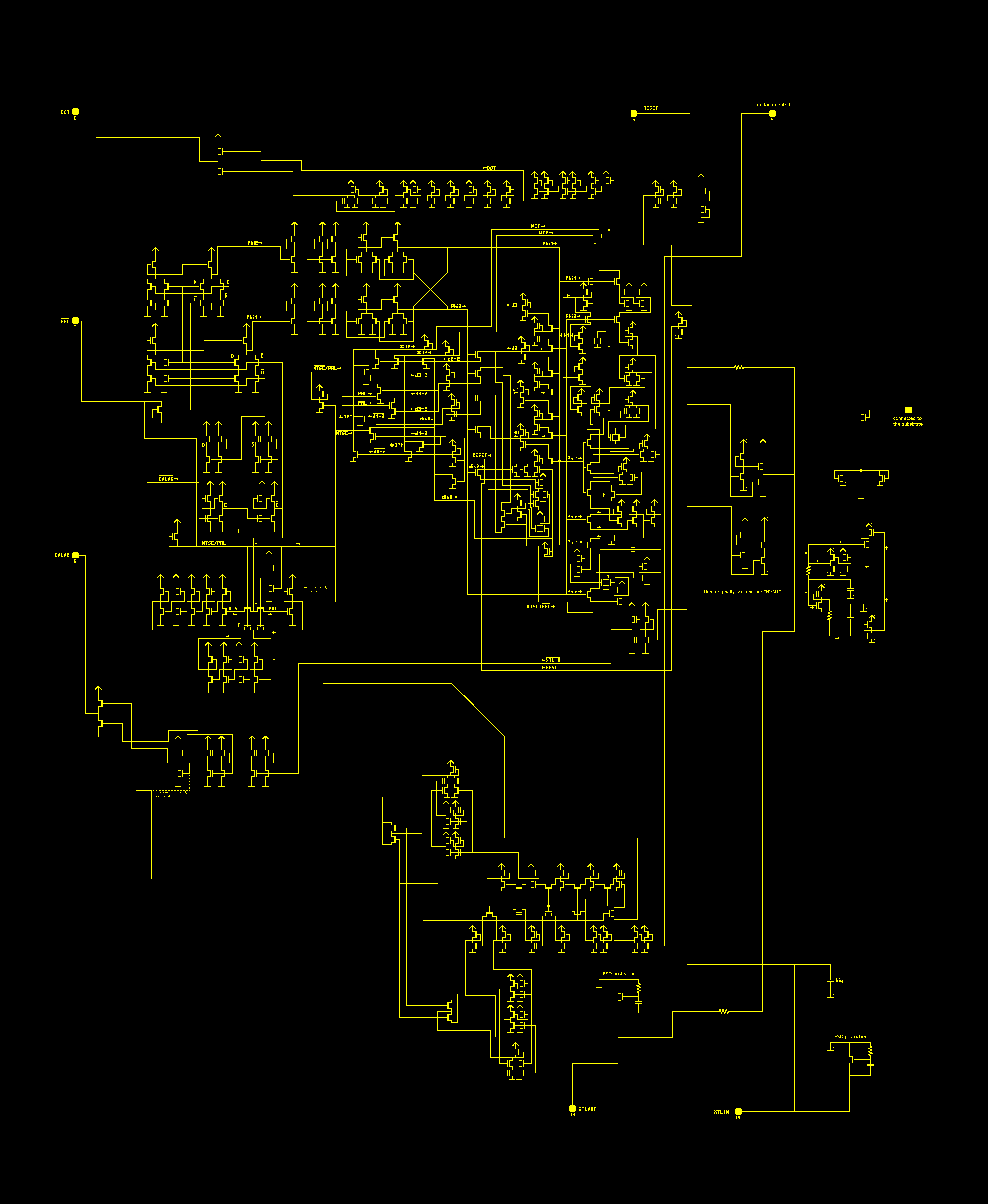
8701_oscillator.png [ 245.36 KiB | Viewed 4803 times ]


Top
 Profile  
Reply with quote  
PostPosted: Mon Sep 24, 2018 11:15 am 
Offline
User avatar

Joined: Thu Dec 11, 2008 1:28 pm
Posts: 10793
Location: England
Very interesting investigations!


Top
 Profile  
Reply with quote  
PostPosted: Mon Sep 24, 2018 11:19 am 
Offline
User avatar

Joined: Fri Nov 09, 2012 5:54 pm
Posts: 1392
Thanks, Ed. :) Just one week and a half of work.

;---

Then we have a superbuffer directly fed by the Crystal input pad:

Attachment:
cclk_sb1.png
cclk_sb1.png [ 7.89 KiB | Viewed 4801 times ]


Which just passes on the inverted oscillator input signal to the Color Clock output buffer.

Attachment:
cclk_out.png
cclk_out.png [ 35.81 KiB | Viewed 4801 times ]


Note the clock signal /color (inverted color clock), which is tapped from the last stage of the Color Clock output buffer.
It is used for generating the Dot Clock later.

Attachment:
8701_colorclock.png
8701_colorclock.png [ 184.1 KiB | Viewed 4801 times ]


Top
 Profile  
Reply with quote  
PostPosted: Mon Sep 24, 2018 11:23 am 
Offline
User avatar

Joined: Fri Nov 09, 2012 5:54 pm
Posts: 1392
When following the /color signal, we enter an area which (from the logic design point of view)
only contains 4 superbuffers:

Attachment:
cdelay2.png
cdelay2.png [ 14.92 KiB | Viewed 4801 times ]


Attachment:
8701_cdelay2.png
8701_cdelay2.png [ 303.96 KiB | Viewed 4801 times ]


Top
 Profile  
Reply with quote  
PostPosted: Mon Sep 24, 2018 11:30 am 
Offline
User avatar

Joined: Fri Nov 09, 2012 5:54 pm
Posts: 1392
Between the area of 4 super buffers and the Color Clock output buffer,
we have an area with delay elements.

Ok, /PAL here is identical to NTSC which is identical to Pin 7 (EnablePAL) of the chip, sorry for the confusion.

Depending on if the chip runs in PAL or NTSC, the delay is selected differently.
There is a reason for this, and don't worry: we are getting there later.

Attachment:
cdelay1.png
cdelay1.png [ 13.9 KiB | Viewed 4799 times ]


Attachment:
8701_cdelay1.png
8701_cdelay1.png [ 243.06 KiB | Viewed 4799 times ]


Oh, and we also have two dead inverters which seem to be leftovers from the PAL delay path in a previous revision of the silicon.


Top
 Profile  
Reply with quote  
PostPosted: Mon Sep 24, 2018 11:35 am 
Offline
User avatar

Joined: Fri Nov 09, 2012 5:54 pm
Posts: 1392
Ok, so North of the area of 4 super buffers, we have two logic gates with a "boosted" output:
an XOR gate, and an XNOR gate.

And yes, we are talking about the clock doubler here.

Attachment:
ckg1.png
ckg1.png [ 24.17 KiB | Viewed 4800 times ]


Attachment:
8701_ckg1.png
8701_ckg1.png [ 190.84 KiB | Viewed 4800 times ]


Top
 Profile  
Reply with quote  
PostPosted: Mon Sep 24, 2018 11:41 am 
Offline
User avatar

Joined: Fri Nov 09, 2012 5:54 pm
Posts: 1392
And (East) from there, generating a two phase non overlapping clock signal PHI1 and PHI2
(to be used for clocking the circuitry which later generates the Dot Clock)
out of the XOR\XNOR output signals PH1 and PH2
just circles around creative tinkering with NOR based RS flipflops:

// I'm intentionally breaking the lines of text this way to prevent a "stack overflow" in the brains of the readers.

Attachment:
ckg2.png
ckg2.png [ 26.42 KiB | Viewed 4800 times ]


Attachment:
8701_ckg2.png
8701_ckg2.png [ 310.07 KiB | Viewed 4800 times ]


Top
 Profile  
Reply with quote  
PostPosted: Mon Sep 24, 2018 11:50 am 
Offline
User avatar

Joined: Fri Nov 09, 2012 5:54 pm
Posts: 1392
The concept for the PHI1, PHI2 clock generation from the Color Clock basically breaks down like this:

Attachment:
8701_clockgenerator.png
8701_clockgenerator.png [ 116.33 KiB | Viewed 4800 times ]


Of course, when building a clock doubler like this, the best approach is to have signal pulses
of half the /color clock period at the outputs of the XOR\XNOR gates.

Color Clock frequency (and period) is different for PAL and NTSC,
and that's why different time delays for PAL and NTSC are used in the clock doubler.

We continue with the circuitry which generates the Dot Clock after a short break...
because that's going to be a lot of stuff.


Top
 Profile  
Reply with quote  
PostPosted: Mon Sep 24, 2018 12:31 pm 
Offline
User avatar

Joined: Fri Nov 09, 2012 5:54 pm
Posts: 1392
I nearly forgot:

Pin 5 is the /RES input, low_active reset signal for the shift register which works as a counter for generating the Dot Clock.

Since there is a pullup resistor inside the chip for Pin 5, Dot Clock generation will work when the pin is not connected (outside the chip).

Attachment:
reset.png
reset.png [ 22.76 KiB | Viewed 4796 times ]


Attachment:
8701_res.png
8701_res.png [ 101.16 KiB | Viewed 4796 times ]


Top
 Profile  
Reply with quote  
PostPosted: Mon Sep 24, 2018 12:37 pm 
Offline
User avatar

Joined: Fri Nov 09, 2012 5:54 pm
Posts: 1392
Ok, now for the hard part:
It's a lot of stuff, and somebody (not me) better should check if I did any mistakes
during reverse_engineering.

The circuitry clocked by PHI1, PHI2 which generates the Dot Clock.

On the silicon, this breaks down into three parts.

First, we have three big NOR gates, plus some and gates and inverters at their inputs:

Attachment:
cnt1.png
cnt1.png [ 54.78 KiB | Viewed 4797 times ]


Attachment:
8701_cnt1.png
8701_cnt1.png [ 259.31 KiB | Viewed 4797 times ]


Top
 Profile  
Reply with quote  
PostPosted: Mon Sep 24, 2018 12:40 pm 
Offline
User avatar

Joined: Fri Nov 09, 2012 5:54 pm
Posts: 1392
Second, we have a shift register which works as a counter.

Attachment:
cnt2.png
cnt2.png [ 23.82 KiB | Viewed 4798 times ]


Attachment:
8701_cnt2_1.png
8701_cnt2_1.png [ 226.54 KiB | Viewed 4798 times ]


Attachment:
8701_cnt2_2.png
8701_cnt2_2.png [ 154.18 KiB | Viewed 4798 times ]


Attachment:
8701_cnt2_3.png
8701_cnt2_3.png [ 257.9 KiB | Viewed 4645 times ]

Edit: error fixed, there were two latches too many in 8701_cnt2_3.


Last edited by ttlworks on Thu Oct 04, 2018 8:00 am, edited 1 time in total.

Top
 Profile  
Reply with quote  
PostPosted: Mon Sep 24, 2018 12:46 pm 
Offline
User avatar

Joined: Fri Nov 09, 2012 5:54 pm
Posts: 1392
Third, we have another shift register plus some logic gates (controlled by the two other blocks mentioned above),
generating a signal which I had named DCLK.
DCLK later goes to the Dot Clock output buffer.

BTW: marking the part of the diffusion layer which happens to be GND with a brighter color sometimes simplifies reverse engineering.

A buried contact in the polygonized images seems to be missing, I had marked the area in question with a little orange rectangle and a question mark.

Attachment:
cnt3.png
cnt3.png [ 27.99 KiB | Viewed 4798 times ]


;---

Attachment:
8701_cnt3_1.png
8701_cnt3_1.png [ 286.07 KiB | Viewed 4798 times ]


;---

Attachment:
8701_cnt3_2.png
8701_cnt3_2.png [ 266.4 KiB | Viewed 4643 times ]

Edit: fixed error: an inverter somehow had sneaked into the input of the #OP NOR gate.

;---

Attachment:
8701_cnt3_3.png
8701_cnt3_3.png [ 157.61 KiB | Viewed 4643 times ]

Edit: fixed.

;---

Attachment:
8701_cnt3_4.png
8701_cnt3_4.png [ 155.8 KiB | Viewed 4643 times ]

Edit: fixed.
Edit2: cleaned up.
...And now the simulation is starting to make sense.


Last edited by ttlworks on Thu Oct 04, 2018 12:51 pm, edited 2 times in total.

Top
 Profile  
Reply with quote  
Display posts from previous:  Sort by  
Post new topic Reply to topic  [ 28 posts ]  Go to page 1, 2  Next

All times are UTC


Who is online

Users browsing this forum: No registered users and 19 guests


You cannot post new topics in this forum
You cannot reply to topics in this forum
You cannot edit your posts in this forum
You cannot delete your posts in this forum
You cannot post attachments in this forum

Search for:
Jump to: