6502.org Forum  Projects  Code  Documents  Tools  Forum
It is currently Tue Apr 30, 2024 5:46 pm

All times are UTC


Post new topic Reply to topic  [ 45 posts ]  Go to page Previous  1, 2, 3
Author Message
PostPosted: Sun Jul 24, 2022 2:14 pm 
Offline
User avatar

Joined: Sun Dec 29, 2002 8:56 pm
Posts: 449
Location: Canada
This circuit born from the following question. (I have not tried it yet).

What if one wanted the number of wait state to vary by chip select, and to have it programmable at run-time?

It is an extension of BDD's wait state generator. Rather than presetting a FF it clears a a shift register whose output is fed to a multiplexor to select the number of wait cycles.
The multiplexor is controlled by the output of a small RAM so the wait state selection can be made programmable. Chip selects drive an encoder to select the RAM address.

Attachment:
File comment: Programmable wait state generator.
WaitStatesN.png
WaitStatesN.png [ 57.58 KiB | Viewed 2685 times ]

_________________
http://www.finitron.ca


Top
 Profile  
Reply with quote  
PostPosted: Mon Jul 25, 2022 2:51 am 
Offline
User avatar

Joined: Thu May 28, 2009 9:46 pm
Posts: 8160
Location: Midwestern USA
It should work, but I think there is far too much prop time in the added parts to get reliable operation at more than 2-3 MHz. 74HC logic is simply too slow. Some of it can be replaced with 74AC or 74AHC logic, which is three times faster. Unfortunately, the 148 encoder is not available in AC or AHC.

_________________
x86?  We ain't got no x86.  We don't NEED no stinking x86!


Last edited by BigDumbDinosaur on Fri Jul 29, 2022 5:37 pm, edited 2 times in total.

Top
 Profile  
Reply with quote  
PostPosted: Sun Jul 31, 2022 11:49 pm 
Offline
User avatar

Joined: Sun Dec 29, 2002 8:56 pm
Posts: 449
Location: Canada
I think the following circuit can be used to stretch the high time of the PH2 clock. It is the high part of the clock that is relied on to generate RD and WR strobes for devices.
A little simpler than the previous circuit. It is programmable via a small memory. It relies on a '163 counter producing a terminal count signal to toggle a FF. When PH2 is high the counter is preset with 14 which causes a terminal count after the next clock pulse. This makes the low time two input clock wide. When PH2 is clocked low, the counter is preset with the value from the RAM. A negative of the desired count should be specified in the RAM.
Attachment:
File comment: PH2 clock stretcher
ClkStretch.png
ClkStretch.png [ 66.43 KiB | Viewed 2591 times ]

_________________
http://www.finitron.ca


Top
 Profile  
Reply with quote  
PostPosted: Mon Nov 06, 2023 12:26 pm 
Offline
User avatar

Joined: Thu May 28, 2009 9:46 pm
Posts: 8160
Location: Midwestern USA
As mentioned a few posts back, the trick of stopping the MPU by controlling the flip-flop generating the Ø2 clock signal does work.  However, the timing deadlines are tight, since they ultimately are relative to the oscillator frequency, which is Ø2 × 2.  I had discussed this timing matter in my POC articles, specifically with testing POC V1.4.  Discussion ensued later on what to do about it.  I’m continuing with that discussion in this topic.

Below is an “improved” clock generator that generates the three clock signals that would be useful in an 816-powered system.  Stretching is done with basic gates, instead of by controlling a flop or a synchronous counter.

Attachment:
File comment: Clock-Stretching Wait-State Circuit
wait_state_test_v2.gif
wait_state_test_v2.gif [ 25.93 KiB | Viewed 2431 times ]

The above circuit is a “proof-of-concept” design and omits some things that would be present in a working example.

In this new design, both sections of the 74AC109 J-K flop are utilized to cause the generator to stretch the clock for either one or two cycles.  The clock source for the AC109 is separate from GCLK, Ø1 and Ø2 so I can experiment with having this clock slightly lag GCLK, as doing so may offer some timing benefits.  It is the 109’s tSU minimum on the /K input that causes wait-stating to mess up in POC V1.3 at Ø2 frequencies beyond 16 MHz.

For testing, I scabbed a circuit from Garth’s website to generate an approximate 1 µsec pulse on the 109’s /K input when the trigger push button is depressed.  This arrangement will eliminate the push button ‘on’ time from the timing picture.  In a practical circuit, /K would be driven by an active-low signal produced in the glue logic when a wait-state is required.

Testing will be tried at a wide range of oscillator frequencies to prove the circuit’s viability.  Since all timing is relative to GCLK, which is the same frequency as the oscillator frequency, the Ø2 “ceiling” should be significantly improved.

Unknowns will be output symmetry and skew between the individual signals.  Symmetry ultimately is dictated by the quality of the oscillator’s output, something that the 74AC74 flop in POC V1.3’s clock circuit effaced.  In practice, asymmetry is usually not a concern until Ø2 gets sufficiently fast to cause an MPU timing violation during one clock phase or the other.  It would be interesting if there were a reasonably simple way to correct an asymmetric clock without any frequency change.

In theory, skew between GCLK and Ø2 should be negligible, since both are generated in the same device.  Skew between Ø1 and Ø2 is more likely to be of significance.  In practice, that may well be of little concern.

Finding out these things will be the purpose of building this test rig.  If it appears to operate as theorized, I have an idea on how to patch it into POC V1.4 to replace the latter’s clock generator circuit, which goes on the fritz at 16 MHz.

_________________
x86?  We ain't got no x86.  We don't NEED no stinking x86!


Top
 Profile  
Reply with quote  
PostPosted: Mon Nov 06, 2023 5:03 pm 
Offline

Joined: Wed Aug 21, 2019 6:10 pm
Posts: 217
GaBuZoMeu wrote:
BigDumbDinosaur wrote:
Both the 65C02 and 65C816 generate the effective address while Ø2 is still low.

Taking the damned DS of the 65C816 tADS is 30 ns for A0:A15 and 33 ns for A16:A23 (tBAS). Cycle time is 35 ns. This would left 5 or 2 ns to setup WSEN. Of course, these are worst case timings but wasn't it you that would go to 20 MHz or more if possible?


Though that is the process that they did the testing for ... it seems a current generation 65C816 is going to have substantially lower delays than that, although the current generation do not sell at the volume to justify the cost of updating the testing. I believe that some people on the site have tested the address and banking setup at around 10ns-12ns, so perhaps 15ns & 16ns is a conservative guess for worst case on the process they are presently using.


Top
 Profile  
Reply with quote  
PostPosted: Tue Nov 07, 2023 1:04 am 
Offline
User avatar

Joined: Thu May 28, 2009 9:46 pm
Posts: 8160
Location: Midwestern USA
BruceRMcF wrote:
GaBuZoMeu wrote:
BigDumbDinosaur wrote:
Both the 65C02 and 65C816 generate the effective address while Ø2 is still low.

Taking the damned DS of the 65C816 tADS is 30 ns for A0:A15 and 33 ns for A16:A23 (tBAS). Cycle time is 35 ns. This would left 5 or 2 ns to setup WSEN. Of course, these are worst case timings but wasn’t it you that would go to 20 MHz or more if possible?

Though that is the process that they did the testing for ... it seems a current generation 65C816 is going to have substantially lower delays than that, although the current generation do not sell at the volume to justify the cost of updating the testing. I believe that some people on the site have tested the address and banking setup at around 10ns-12ns, so perhaps 15ns & 16ns is a conservative guess for worst case on the process they are presently using.

Current production dice are fabbed at TSMC, using 0.6µ geometry.  Production testing is done at 20 MHz.  I was told some time ago by David Gray at WDC that a device must function at 20 MHz to be considered saleable.  That parts must work at 20 MHz seems to imply that the timing values listed in the current data sheets are excessively pessimistic.

My testing of several 65C816s in POC V1.3 indicate that addresses become valid around 12ns after the fall of Ø2.  At 20 MHz, that means addresses are valid about 13ns before Ø2 goes high.  A 74AC or 74AHC bank latch can easily handle that timing window.

_________________
x86?  We ain't got no x86.  We don't NEED no stinking x86!


Top
 Profile  
Reply with quote  
PostPosted: Tue Nov 07, 2023 8:45 am 
Offline
User avatar

Joined: Thu Dec 11, 2008 1:28 pm
Posts: 10793
Location: England
> Production testing is done at 20 MHz. I was told some time ago by David Gray at WDC that a device must function at 20 MHz to be considered saleable.

Although it's good that silicon is coming out comfortably within spec, one shouldn't read too much into testing at 20MHz. There are various reasons which come down to uncertainties and margin
- can't test every internal path
- probably not testing at high temperature
- possibly need some margin for noise and jitter which would exist in use but absent in testing

On the other hand, testing every part does mean that they take into account process variation (whereas the hobbyist is sampling an unknown distribution), and surely they also test at minimum supply voltage, and perhaps slowest permissible input slew rates.


Top
 Profile  
Reply with quote  
PostPosted: Wed Nov 08, 2023 2:15 am 
Offline
User avatar

Joined: Thu May 28, 2009 9:46 pm
Posts: 8160
Location: Midwestern USA
BigDumbDinosaur wrote:
Below is an “improved” clock generator that generates the three clock signals that would be useful in an 816-powered system...

I got busy and did a PCB layout for this thing.  Needless to say, with such a simple circuit, the layout was not much of a challenge.  I did not go for the tightest possible layout, mostly because there was no need for it, and also because I have to be able to build this thing looking through one eye.  :roll:  So I went with DIP parts and 0.100" (2.54mm) hole spacing.

The board has a couple of minor additions over what I show in the previously-posted schematic.  I added series resistance to the clock outputs and inserted a jumper block (JP3) into the trigger circuit to allow me to isolate the trigger output of the Schmitt inverter from the 74AC109’s /K input.  These changes are in anticipation of trying to monkey-rig this gadget into POC V1.4’s clock-generation circuit.

Attachment:
File comment: Wait-State Test Rig
wait_state_test_v2_pcb.gif
wait_state_test_v2_pcb.gif [ 63.14 KiB | Viewed 2325 times ]

For reference, it’s a four-layer PCB and its dimensions are 3.50" × 1.88" (88.90mm × 47.63mm).  In case you are wondering about the size of the bypass capacitors, I have a bunch of them in my junk and decided it was time to use them up.

I expect the cost to ship these boards from JLCPCB will be much greater than the cost to have them made.  :D  I remember when it was the other way around, and some PCBs of this size would run at least 400USD—much of it setup cost, with negligible shipping cost.

_________________
x86?  We ain't got no x86.  We don't NEED no stinking x86!


Top
 Profile  
Reply with quote  
PostPosted: Mon Nov 20, 2023 10:41 pm 
Offline
User avatar

Joined: Thu May 28, 2009 9:46 pm
Posts: 8160
Location: Midwestern USA
I’ve ordered parts for the new clock-stretcher design, but have yet to order the PCBs.  Too many things have been conspiring to steal my time, not the least of which is a client who has a tendency to do stupid stuff with his computer system.  :D  I hope to get back on this mini-project real soon.

_________________
x86?  We ain't got no x86.  We don't NEED no stinking x86!


Top
 Profile  
Reply with quote  
PostPosted: Tue Nov 21, 2023 7:34 pm 
Offline
User avatar

Joined: Thu May 28, 2009 9:46 pm
Posts: 8160
Location: Midwestern USA
While I am waiting for parts to arrive, I made a design change, which was to add clamping diodes to the three clock outputs to help suppress ringing.  During initial testing, I will leave these out to get a baseline picture of the clocks’ waveforms.  After that, I’ll add the diodes to see what effect, if any, they might have.

BTW, the schematic says the clamping diodes are SD103A.  The part I will be using is BAT85, which has a shorter recovery time and a slightly smaller package.

Attachment:
File comment: Wait-State Test Rig Schematic
wait_state_test_v2.pdf [49.48 KiB]
Downloaded 47 times
Attachment:
File comment: Wait-State Test Rig PCB Layout
wait_state_test_v2_pcb.gif
wait_state_test_v2_pcb.gif [ 104.22 KiB | Viewed 2220 times ]

PCB size is 3.69" × 1.88", or 93.7mm × 47.6mm.

_________________
x86?  We ain't got no x86.  We don't NEED no stinking x86!


Top
 Profile  
Reply with quote  
PostPosted: Fri Dec 01, 2023 9:07 pm 
Offline
User avatar

Joined: Thu May 28, 2009 9:46 pm
Posts: 8160
Location: Midwestern USA
BigDumbDinosaur wrote:
While I am waiting for parts to arrive...

All parts have arrived.  Now, all I gotta do is find some time to build and test this contraption.  Maybe tonight after the 10 o’clock news...  :D

_________________
x86?  We ain't got no x86.  We don't NEED no stinking x86!


Top
 Profile  
Reply with quote  
PostPosted: Tue Dec 05, 2023 8:36 am 
Offline
User avatar

Joined: Thu May 28, 2009 9:46 pm
Posts: 8160
Location: Midwestern USA
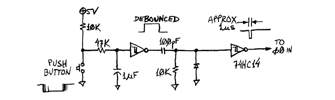
BigDumbDinosaur wrote:
All parts have arrived.  Now, all I gotta do is find some time to build and test this contraption.  Maybe tonight after the 10 o’clock news...  :D

The test rig has been built and tested.  For some completely unfathomable reason, it functions exactly as intended.  :shock:  First, here is a photo I took of the unit after hooking it up to the logic analyzer:

Attachment:
File comment: Test Rig Connected to Logic Analyzer
wait_state_test_rig_v2_02.gif
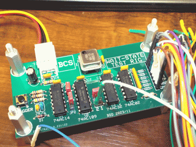
wait_state_test_rig_v2_02.gif [ 1.3 MiB | Viewed 1914 times ]

When the push button at the left end of the unit is pressed, a 1 µsec pulse will be generated to start the wait-state cycle.  I shamelessly “borrowed” the pulse-generator circuit from Garth’s clock page on his website.  :P  For the record, the observed pulse duration is 1.036 µsecs.  :D

The observant will notice that I haven’t installed the output clamping diodes.  For some reason, I thought I had some BAT85s in my parts pile, but that wasn’t the case.  All I had were some SD103s, which with a 10ns TRR, aren’t fast enough.  I’ll get some BAT85s with the next parts order and will subsequently post before-and-after photos of what the clock outputs look like on the scope.

I did scope the clock outputs to verify amplitude and waveform.  There’s a tad bit of ringing, which is to be expected with the extremely fast edges emitted by 74AC devices.  The ringing is more pronounced on the upstream side of the resistor network that drives the outputs, which tells me series resistance is helping.  It’ll be interesting to see what the clamping diodes do.

Meanwhile, I ran some logic analyzer tests to see if theory and practice were approximately the same.  See here for the test rig’s schematic.  Signals being observed in the tests are:

  • Global clock, aka GCLK.  All timing is referenced to GCLK, which runs at the same speed as the oscillator and is never stretched.

    Something worth noting: in this circuit, clock symmetry is exactly the same as the oscillator’s.  Typically, 100 PPM can oscillators have a duty cycle rating that ranges from 47-53 to 53-47.  A system clocked by an asymmetric oscillator and running close to the limits of the MPU can fall victim to difficult-to-diagnose timing violations.  I’ll talk a bit more about this later on.

  • Timing clock, aka TCLKTCLK is the clock source for the 74AC109 timing flip-flop that controls stretching, and is derived from GCLK.  As I surmised that there might be some benefit to having TCLK slightly lag GCLK, I rigged up a jumper block on the board so I could directly drive TCLK from GCLK, or add some lag to TCLK by inserting one or two gates into the signal path.

  • Ø1 & Ø2Ø1 and Ø2 are stretched whenever a wait-state is needed.  In a 65C02 system, Ø1 is unlikely to be needed, but would be useful with a 65C816 to gate the bank latch and data bus transceiver.

  • Wait-state enable, aka /WSE.  In the test rig, /WSE is driven by a Schmitt inverter that is part of the pulse generator circuit.  In a practical application, the glue logic would drive this signal low when a wait-state is required.

  • Stop, aka STP.  This signal is the /Q output of the AC109 timing flop—STP is actually high-true.  I sampled it with the logic analyzer to gain a feel for how long it would take the flop to “wake up” after /WSE was asserted.

Before continuing, I must note that the logic analyzer has a 2ns resolution, which means some timing results need to be taken with a grain of salt, especially at the higher clock rates.  In an effort to make things look as realistic as possible, I set the logic analyzer’s notion of where a logic transition occurs at VCC × 0.5, VCC being 5 volts (measured voltage at the input connector was 5.03).  The set logic transition point definitely affects how the logic analyzer fudges some timing numbers.

Here are the test results.

Attachment:
File comment: Running @ 1 MHz, 1 Wait-State
wait_state_v2_01mhz_1ws.gif
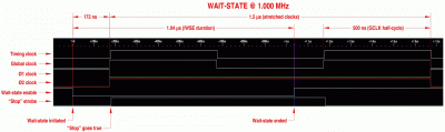
wait_state_v2_01mhz_1ws.gif [ 48.97 KiB | Viewed 1914 times ]

Above is a run with a 1 MHz oscillator in the test rig, and the rig configured to generate one wait-state.  It can be seen that Ø1 and Ø2 are stretched by one extra GCLK cycle.  It’s not readily observable in this run or the next one, but there is a slight lag between GCLK and TCLK.

Attachment:
File comment: Running @ 1 MHz, 2 Wait-States
wait_state_v2_01mhz_2ws.gif
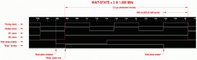
wait_state_v2_01mhz_2ws.gif [ 55.18 KiB | Viewed 1914 times ]

Above is another run with the 1 MHz oscillator, but with the rig configured to generate two wait-states.

The purpose of this run and the previous one was to prove that the circuit functions as intended.  In a practical sense, a 1 MHz system should not ever need wait-stating,  given the speeds of modern hardware.  Needless to say, two wait-states at 1 MHz would be gross overkill with just about any hardware we might ever use, even 1970s-vintage parts.  However, as will soon be seen, this circuit can be run at much higher speeds, at which time, two wait-states might come in handy.

Attachment:
File comment: Running @ 20 MHz, 1 Wait-State
wait_state_v2_20mhz.gif
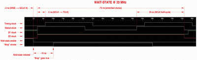
wait_state_v2_20mhz.gif [ 49.79 KiB | Viewed 1914 times ]

Above is a run at 20 MHz, with the rig configured to generate one wait-state.  There is plenty of timing head room available.  The lag between GCLK and TCLK is clearly visible.

Attachment:
File comment: Running @ 40 MHz, 1 Wait-State
wait_state_v2_40mhz.gif
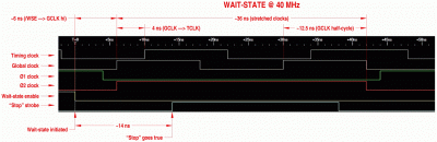
wait_state_v2_40mhz.gif [ 53.79 KiB | Viewed 1914 times ]

Above is a run at 40 MHz, also with the rig configured to generate one wait-state.  There is still some timing head room available and, in fact, the numbers suggest the circuit would be reliable to at least 60 MHz.  Fudging effects by the logic analyzer are obvious, in that it appears Ø1 and Ø2 are rising and falling at different times.  Observation with the scope (275 MHz) indicates that the two signals are in step.

Some notes:

  • In all of the above runs, TCLK is configured to maximally lag GCLK—there are two gate delays between the latter and the former.  However, the total lag is small, as it turns out the OR gates through which TCLK is derived are substantially faster than the data sheet lets on.  Obviously, that lag could vary with different parts, and definitely would be greater at a lower VCC, but I suspect modern iterations of 74AC logic have gotten substantially faster with improved wafer fabricating processes.

  • Observed clock symmetry varied from one oscillator to another.  However, that observation needs to be considered against fudging effects by the logic analyzer.  Fudging is especially noticeable when an interval being observed is not evenly divisible by 2.  At maximum resolution, the logic analyzer will round things to the nearest 2 ns, which may cause symmetric signals to appear asymmetric.  For example, the clock phase period at 40 MHz is 12.5 ns.  The limits of the logic analyzer’s resolution would represent that as 12 ns, causing the 40 MHz clock to “look funny.”

  • As the AC109 timing flop is clocked at the same frequency as GCLK and the unstretched Ø1 and Ø2 clocks, gating the flop’s /K input by /WSE is not nearly as timing-critical as is the case with the circuit I presented much earlier in this topic.  In that circuit, the reference clock is the oscillator, which runs at twice the speed of GCLK, making the available timing window a lot smaller.  In this circuit, as long as /WSE goes low at least TSU nanosecs (~5 ns minimum with a 74AC109 at 5 volts) before the rise of TCLK, the circuit should be reliable.

  • A solution to dealing with oscillator asymmetry in a “ragged-edge” application would be to pass the oscillator’s output through a flop.  That flop would solely function to produce a symmetric clock to the gates that make up the rest of this circuit.  Obviously, the oscillator would have to run at twice the desired clock rate.

  • There may be some other permutations of this circuit that I may explore.  They have yet to gel in my mind, likely due to me being a old curmudgeon whose brain is slowly wasting away.  :D

_________________
x86?  We ain't got no x86.  We don't NEED no stinking x86!


Top
 Profile  
Reply with quote  
PostPosted: Fri Dec 22, 2023 1:18 am 
Offline
User avatar

Joined: Thu May 28, 2009 9:46 pm
Posts: 8160
Location: Midwestern USA
BigDumbDinosaur wrote:
  • There may be some other permutations of this circuit that I may explore.  They have yet to gel in my mind, likely due to me being a old curmudgeon whose brain is slowly wasting away.  :D

Brain rot aside, I did come up with an alternate permutation that deals with the possibility of oscillator output asymmetry.  This one runs the oscillator’s signal through a 74AC74 flip-flop.

Also, to be different than the earlier circuit, Ø1 is derived off the flop’s /Q output and is run through an AND gate for control.  There may be some benefit to doing so to minimize skew between Ø1 and Ø2, since the AND gate has essentially the same prop time characteristics as the OR gate through which GCLK and Ø2 are derived.  This is in contrast to the NOR gate I used in the earlier design, which is a teensy bit slower overall.

I haven’t decided yet as to whether I should prototype it and do some more testing.

Attachment:
File comment: Yet Another Clock Generator
clock_gen_ff_gates.gif
clock_gen_ff_gates.gif [ 40.12 KiB | Viewed 1470 times ]

_________________
x86?  We ain't got no x86.  We don't NEED no stinking x86!


Top
 Profile  
Reply with quote  
PostPosted: Fri Dec 22, 2023 4:59 am 
Offline

Joined: Fri Jul 09, 2021 10:12 pm
Posts: 741
Have you tried hooking it up to one of the POCs yet, or is that the next step? I think it will work well, and I'm not sure that asymmetry is inherently a problem - more that there's some lower limit for each phase of the clock, and I don't think they're necessarily the same. So if the clock is asymmetric, then inverting it might give the problem phase a bit longer to do its work. I did try to test this, with the 65C02, but only really concluded that there's no low-hanging fruit - significant changes to the duty cycle didn't affect the maximum speed in a way that I could easily detect. It got to the point where it took several hours of soak testing to observe a failure, and I didn't have the time or patience to continue testing it rigorously!


Top
 Profile  
Reply with quote  
PostPosted: Fri Dec 22, 2023 7:23 am 
Offline
User avatar

Joined: Thu May 28, 2009 9:46 pm
Posts: 8160
Location: Midwestern USA
gfoot wrote:
Have you tried hooking it up to one of the POCs yet, or is that the next step?

I’ve been mulling two different methods of running a real-world test.

  1. Butcher up POC V1.3 to get its clocks from the test rig.

    Butchering V1.3 shouldn’t be too difficult or extensive, thanks to the use of some discrete resistors in series with the Ø1 and Ø2 clock signal lines.  If I remove those resistors, Ø1 and Ø2 will be isolated from the on-board clock generator, which means I can bodge-wire the clock lines over to the test rig and not have to desolder the clock generator chips.

    Another bodge wire would be needed to connect the /WSE circuit on the test rig into /WSE on V1.3.  I’d also bodge-wire a ground between the test rig and V1.3, even though both will be getting power from the same power supply.  Otherwise, I might end up with a “dirty” clock signal.  An alternative to that would be to have the test rig draw its power from V1.3, which would avoid possible problems from ground looping.

    As V1.3’s clock “service ceiling” is 16 MHz (due to timing constraints in the existing wait-state circuitry), I’d immediately know things are on the right track if I can get it running at 20 MHz...or faster.  :D

  2. Design and build a new computer that uses the new-fangled clock circuit.

    I have been thinking on-and-off about designing a 512KB version of POC V1.3, which would be an all-discrete design with the logic needed to handle more extended RAM.  Something that had stopped me from doing so was the problem of detecting an effective address in bank zero to prevent mirroring of ROM and I/O in other banks.  That’s not as simple as in V1.3, as the latter has only one extended address line (A16).

    A 512KB unit would have A16, A17 and A18.  The problem is in detecting when the expression !(A16 & A17 & A18) & (VDA | VPA) is true using only discrete logic, and doing it with a minimum of delay.  Detection methods I had devised in the past resulted in too much prop delay through the glue logic to be workable much above 10 MHz.  However, I recently conjured what I think may be a workable solution, which would open the door to having multiple extended RAM banks without having to pile on the glue logic.  I’ve made some sketches of a possible circuit, but need to do a timing analysis before I decide if it is a viable design.

Naturally, method A would be much more expedient, and I think would be the logical route to follow for now.  Its only downside, aside from the potential of inadvertently wrecking the only working specimen of POC V1.3, would be in the effects of not having a bus transceiver on the data lines.  Without the bus transceiver, the potential for momentary bus contention right after the rise of the clock will be present and could prove fatal as the clock gets ramped up.

Quote:
I think it will work well...

The logic analysis did look promising at 40 MHz—there was adequate timing headroom.  The key to it is the fact that the wait-state timing clock slightly lags the global clock.  That produces a little more setup time for the wait-state flop (the AC109) to react to /WSE going low.  I’m pretty confident that it will do fine at a more sedate clock rate.

Quote:
...and I’m not sure that asymmetry is inherently a problem...

The asymmetry thing should only become worrisome if the Ø2 rate is close to the MPU’s limits.  Plasmo reported that he has not used a flop to deal with asymmetry in the clock circuit of any of his high speed experiments.  So my concern is more theoretical than actual.  I’ll worry about it when I get a system running at 40 MHz.  :D

That said, using the flop version of the clock circuit would reduce the potential for skew to occur between Ø1 and Ø2.  Such skew in a 65C816 circuit running near the max might cause trouble with the bank latch.  However, at this point in time, I don’t know where “the max” is.

_________________
x86?  We ain't got no x86.  We don't NEED no stinking x86!


Top
 Profile  
Reply with quote  
Display posts from previous:  Sort by  
Post new topic Reply to topic  [ 45 posts ]  Go to page Previous  1, 2, 3

All times are UTC


Who is online

Users browsing this forum: No registered users and 31 guests


You cannot post new topics in this forum
You cannot reply to topics in this forum
You cannot edit your posts in this forum
You cannot delete your posts in this forum
You cannot post attachments in this forum

Search for:
Jump to: