6502.org Forum  Projects  Code  Documents  Tools  Forum
It is currently Mon Apr 29, 2024 1:55 pm

All times are UTC


Post new topic Reply to topic  [ 7 posts ] 
Author Message
PostPosted: Sun Mar 11, 2018 1:26 pm 
Offline

Joined: Sat Jan 02, 2016 10:22 am
Posts: 197
I've been given some re-marked CPU's to play with, and I've been trying to work out what they really are.

Attachment:
File comment: 4 NOS devices all with the same lot code, and only 1 set of mould marks. Hmmmmm
re-marked chips.jpg
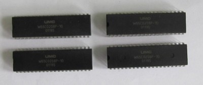
re-marked chips.jpg [ 26.55 KiB | Viewed 3335 times ]


One thing they're not is CMOS 65C02s, of the 4, 3 will start up and run 6502 code on a test board. All 3 exhibit the JMP (xxFF) bug so have an NMOS core of some description. The test board is wired for a modern W65C02, but has an additional jumper to add 0v to pin 1 in place of VP.

Attachment:
File comment: Reverse view is interesting
under sides.jpg
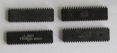
under sides.jpg [ 34.38 KiB | Viewed 3335 times ]


The under side shows how little care was taken with the re-marking. While the top's been sanded and etched, they've not bothered to "clean up" underneath.

Top left, with no rear markings, that's one of the one's that works, it ran the basic diagnostics at 1 and 4mhz. Other than knowing it's NMOS, and probably a 2mhz part, there probably not much more can be found out.

Top right, that's the one that doesn't work in the test board, with or without 0v on pin 1. The markings are interesting, the look like something Rockwell might have printed, but R6502F ? Close up, the print looks old, the solder splashes and marks from the removal process go over the print. There's no evidence I can see that the last letter is misprinted or altered. I could be underneath it's nothing like a 6502 CPU, or it is (was), and is dead. If it is a custom 6502 design of some type, it might be interesting to find out more.

Bottom left, the printing matches a picture I found of the SYU6502A. Like the others, tested as NMOS and ran at 1 and surprisingly since that's a 2mhz part, it completed the tests at 4mhz.

Bottom right, the only one with mould marks, the text font and format look like something out of CSG but I've not located any pictures with a close match to make a guess as to which one of the myriad of CPU versions it is. It runs the test code at 1, 2 and 4mhz. No surprise that it failed a 6mhz.

So:
Any ideas about how to identify the "CSG" chip if that's what it is
Likewise the "R6502F"

The test board is point to point soldered, so wiring up additional pins isn't a problem.


Top
 Profile  
Reply with quote  
PostPosted: Sun Mar 11, 2018 1:43 pm 
Offline
User avatar

Joined: Thu Dec 11, 2008 1:28 pm
Posts: 10793
Location: England
Perhaps run a hard-wired NOP test and check for activity on Sync and the address pins. Perhaps some other opcode and watch RnW. Check the power consumption? Does the clock output wiggle as it should?

(I'm thinking it could be anything at all, not even a CPU. In which case which pins are the power pins is up for grabs.)


Top
 Profile  
Reply with quote  
PostPosted: Mon Mar 12, 2018 10:36 pm 
Offline

Joined: Sat Jan 02, 2016 10:22 am
Posts: 197
I've had time to do some of the suggestions.

NOP "rom" fitted and the ram on the test board removed. The address bus is wiggling at what looks like the correct rate. A0 is cycling at 500khz with a 2mhz clock fitted. A1 at 250khz etc.

So maybe it really is a 6502 of some kind.

Hooked up a cheapo 8 channel USB logic analyser to A0-A7 and read off the hex values.

It was E9 while at reset, then when reset came up I got 00, FF, FE, FC, FD, EA, then EB, EC, ED etc at half the rate of the first few values.

If I'm understanding the 6502 reset process right, that could be 3 stack pushes at 0100,01FF and 01FE, followed by the reset vector being read from FFFC and FFFD, then its counting up from EAEA at half rate because it's running 2 cycle NOPs.

In which case it quite likely IS a 6502 or close relative, but it doesn't explain why the test rom doesn't produce any output on display, when a regular 6502 does.

Start sampling the other pins next time I guess?


Top
 Profile  
Reply with quote  
PostPosted: Tue Mar 13, 2018 12:22 pm 
Offline
User avatar

Joined: Thu Dec 11, 2008 1:28 pm
Posts: 10793
Location: England
Interesting - it does seem somewhat like a 6502! If you have a few more channels, you could run hoglet's 6502 protocol decoder. I think these days you can make do with fewer than 12, but you do need more than 8.
viewtopic.php?f=4&t=4963


Top
 Profile  
Reply with quote  
PostPosted: Wed Mar 14, 2018 8:10 pm 
Offline

Joined: Sat Jan 02, 2016 10:22 am
Posts: 197
8 channels only I'm afraid.

Checking the pins things look very 6502 like.

Pin 39 produces a square wave following the clock input on pin 37, Pin 3 outputs the inverted square wave.

I did several runs covering the data bus, low 8 bits address bus and control bits.

What I got was
Code:
address byte
xx00    BC
xxFF    01
xxFE    FA   - reset sequence RW was high
xxFC    EA
xxFD    C1   - The reset code in the rom is at C1EA
xxE2    4F   - these 3 bytes are in the rom at C1E2
xxE3    53
xxE4    20
xx53    F1   - writing to address 2053 I guess as RW goes low briefly around here
xx53    F7
xx53    73
xxE5    52   - Back to the rom at C1E5
xxE6    4F
xxFF    C4
xxFE    7B
xxFF    stuck address bus


It looks like yes, it IS a 6502, but there's something broken internally, as the reset vector it fetched correctly, but the address the program counter accessed was different. As it fell over trying to run a text string ("OS ROM").

One for the bin I think, unless there's a better sugestion!


Top
 Profile  
Reply with quote  
PostPosted: Wed Mar 14, 2018 10:30 pm 
Offline
User avatar

Joined: Thu Dec 11, 2008 1:28 pm
Posts: 10793
Location: England
I wonder if it's seeing bit 3 stuck low. Could it have a dirty pin, or might the breakage be internal?


Top
 Profile  
Reply with quote  
PostPosted: Thu Mar 15, 2018 1:34 pm 
Offline

Joined: Sat Jan 02, 2016 10:22 am
Posts: 197
Best guess, is that it's something internal.

I wrote a test rom that I could follow on the address bus that was simply

Code:
org &C000
.start
ldx #&FF
TXS
jsr test
jmp start

org &E2E2
.test
RTS


Tje JSR test address was pick as E2 is an address that works.

Running that I could follow on the analyser as the code looped. The only bit that wasn't 100% as per the code was the push values in the JSR, as they were F7 and F6. So same as the reset vector where it use E2 instead of EA that appears to be bit 3 stuck low.

However address bit 3 is high for the reset vector, and low for the reset address which suggests the A3 pin is fine. Bit 3 also high in the TXS opcode, so pin D3 is probably OK too.

I re-did the code with LDX #&F7 followed by 8x INX, when the push happened on that version, FF and FE appear on the trace.

Since it does run 6502 code, I don't think doubt it is a member of the 6502 family.

But something internal is messed up.


Top
 Profile  
Reply with quote  
Display posts from previous:  Sort by  
Post new topic Reply to topic  [ 7 posts ] 

All times are UTC


Who is online

Users browsing this forum: Google [Bot] and 32 guests


You cannot post new topics in this forum
You cannot reply to topics in this forum
You cannot edit your posts in this forum
You cannot delete your posts in this forum
You cannot post attachments in this forum

Search for:
Jump to: