6502.org Forum  Projects  Code  Documents  Tools  Forum
It is currently Fri Apr 26, 2024 8:59 am

All times are UTC


Post new topic Reply to topic  [ 4 posts ] 
Author Message
PostPosted: Sat Nov 18, 2017 4:42 pm 
Offline

Joined: Fri Jul 22, 2016 2:05 pm
Posts: 8
Hello everyone!

1 year or so I wrote a post asking for help in finding a way to output video for my 6502 based computer project. I got many good suggestions, and I've succesfully implemented a composite video output using an ATMEL ATMega328. Now I was thinking of some way of achieving a similar result, without using the ATMega chip. I've studied Don Lancaster's Cheap Video approach of the TVT-6 and found it very interesting. At first I was thinking about implementing that solution, but I then decided to try an approach in which video timing is not generated by the processor. I then proceeded studying the use of the Motorola MC6845 and found many good hints and suggestions. I was thinking about using that chip too, but it is a bit difficult to find and most probably it will be even more so in the future.

I then decided to take a different approach at it and design a circuit which uses only TTL logic and some ROM chips. As I'm a complete newbie, it may be that either this idea is total garbage, or has already be done before. I would like you to help me understand if it is doable, makes sense, and if it is actually any good :) .

My design started from the project "specifications". What I wanted to achieve was a PAL non-interlace monocrome composite output capable of showing on screen at least a standard 40x24 8x8 characters. I then started looking at the PAL timings, which allocate a total of 52us for each visible line. As 40x8 is 320 pixels per line, this means that each pixel takes around 162.5ns to be displayed. I then decided that a pixel output rate of 8MHz, i.e. 125ns per pixel, should be enough and much easier to achieve in practice.

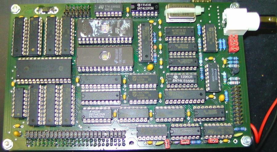
To generate the video signal, I deviced the attached conceptual circuit. Its operation is as follows:

1. a 8MHz clock source is used. It directly drives the shift register for the video output, and also drives the 6502 and the rest of the circuit, after being demultiplied by 8 times to 1MHz.
2. the 1MHz clock drives a 14 bit address counter. Its output, through an offset which maps it to the video memory location, is directly connected to the 6502 address bus. Similar to other implementations, the video circuit RAM access happens during Phi1, thus not interfering with the normal address bus access of the processor.
3. the counter output is also used to access a "sync ROM". As both horizontal and vertical sync signals used in PAL composite video are at least 2us long, this means that the 1MHz output rate of this ROM is capable of driving them. The sync ROM only uses 2 of its 8 bits. One bit is the sync signal, while the other is the frame end signal. When the last byte of the last line is drawn, the frame end signal is dispatched, resetting the address counter. This happens every 312 x 64 bytes of shown data, which at 1MHz is equal to 19.968ms, or 50.08Hz, close enough for the PAL signal.
4. the RAM outputs the required 8 bits of video memory in parallel. The 8MHz shift register serializes them and outputs the required video signal.
5. the sync and video signals are mixed using a 470 and 1k resistors, producing the required composite output.


As an example, the horizontal sync signal is a 4us long low pulse followed by an high value for the remaining 60us that make up the total 64us line length. To represent this signal in the sync ROM, the sync bit must output the following stream of values:

00001111....1111 <--- total of 64 bits

The main drawback of this approach, other than the fact that video and system RAM are shared, is that RAM space must also be allocated for non-visible pixels, for a total of 312x64 ~= 20k. Some additional hardware may allow to store only the visible bytes, i.e. 304x52 ~= 16k.

As is, this solution is suitable for graphic output. The use of some more logic and a character generator ROM may allow to use it for purely text output.

Do you think this may work, and makes any sense? I still have some doubts regarding specific timings, in particular for the shift register, as I'm not sure how to handle the load cycle. But before I dwell in those matters more deeply, I would like to hear your opinion.

I must specify that all of this project is purely "academic". I know there are better, faster, and more efficient solutions.

Thank you for your help and attention! :)

Cheers,
Davide


Attachments:
video_generator.png
video_generator.png [ 40.54 KiB | Viewed 3392 times ]
Top
 Profile  
Reply with quote  
PostPosted: Sat Nov 18, 2017 7:42 pm 
Offline
User avatar

Joined: Fri Aug 30, 2002 9:02 pm
Posts: 1681
Location: Sacramento, CA
Hi Davide,

Yes, your concept will work. There are ways to reduce RAM usage at the cost of more hardware. I attempted a similar TTL solution many years ago but decided to use a microcontroller instead. If you start your counter at the first active row, then you will only require 12K of RAM if you use the ROM to control the pixel output during no-active time. All of the lines above 192, 193-312 are used for bottom blank space, vertical sync, and top blank space. Again, using the ROM to control the pixel output will allow the RAM addressed during that time to be used for program/data storage. So only 12,288 (64x8x24) bytes need to be used. The RAM at the end of each line (41-64), can also be used by programs for data storage. If I recall, the Apple ][ has 8 bytes of dead space at the end of each line that you could use.

ROM control could be done with an AND gate connected to the output of the shift register and the ROM drive pin. A 1 from the ROM would pass the shift register out. A 0 from the ROM would hold the output low.

I used a 74HC165 shift register for my pixel clock on my first display. It worked well with the microcontroller running the /PL pin and the bit clock driving the clock pin. I'm sure you will find a way to shift the data.

Good luck with your project if you decide to move forward.

Daryl

_________________
Please visit my website -> https://sbc.rictor.org/


Last edited by 8BIT on Sat Jun 27, 2020 8:50 pm, edited 1 time in total.

Top
 Profile  
Reply with quote  
PostPosted: Mon Nov 20, 2017 3:08 pm 
Offline
User avatar

Joined: Wed Aug 17, 2005 12:07 am
Posts: 1207
Location: Soddy-Daisy, TN USA
This is a similar concept to what the Parallax Propeller does. It uses ROM (many times) to generate sync pulses and data.

For example, the hsync could be something like 01 00 01 01 in pixel values.

@8BIT, the extra RAM in the Apple II display are called "Screen holes". :-)

https://en.wikipedia.org/wiki/Apple_II_graphics

_________________
Cat; the other white meat.


Top
 Profile  
Reply with quote  
PostPosted: Mon Nov 20, 2017 6:03 pm 
Offline
User avatar

Joined: Fri Nov 09, 2012 5:54 pm
Posts: 1392
Back in 2013, I did a TTL based CRT controller, monochrome 40*25 text and something like C64 HIRES graphics.
A 15 Bit counter (2*74393) running at 1 MHz was feeding a 27512 EPROM which generated control signals
(including sync signals) and the display address. (EPROM was read at 2 MHz to give 16 Bit per microsecond.)

It was able to display text and graphics simultaneously, and to drive a CRT and a LCD in parallel.

Image

http://6502.org/users/dieter/drc2/drc2.htm
Scroll down the page to the D04 block diagram.

About the RAM:
D04 passively scanned the 6502 bus for write cycles in the address range $0400..$07FF.
When detecting such a write cycle, D04 kept data and address in latches and wrote/mirrored
the data in the right moment into the 32kB on_board display RAM.

Point is, that outside the stack area, the 6502 won't do successive write cycles.
The worst caste scenario is code like
STA $0400
STA $0401
what means three read cycles followed by one write cycle.
So if the display RAM is written at only 1MB/sec., running the 6502 at 3MHz will work.

Of course, when building this contraption I didn't know about 6502 bus timing what I know now,
so I would recommend to implement the bus interface of the display controller a little bit different
than I did.

Hope, this helps.


Top
 Profile  
Reply with quote  
Display posts from previous:  Sort by  
Post new topic Reply to topic  [ 4 posts ] 

All times are UTC


Who is online

Users browsing this forum: Google [Bot] and 35 guests


You cannot post new topics in this forum
You cannot reply to topics in this forum
You cannot edit your posts in this forum
You cannot delete your posts in this forum
You cannot post attachments in this forum

Search for:
Jump to: