6502.org Forum  Projects  Code  Documents  Tools  Forum
It is currently Thu May 02, 2024 4:58 am

All times are UTC


Post new topic Reply to topic  [ 115 posts ]  Go to page Previous  1 ... 4, 5, 6, 7, 8
Author Message
PostPosted: Thu Dec 14, 2017 2:30 pm 
Offline
User avatar

Joined: Fri Nov 09, 2012 5:54 pm
Posts: 1392
Thanks for the link...
...so the latest news on the Potato Semi homepage seems to be from 2010.

Now that you had mentioned "No static current":
Would be interesting to see a "supply current versus clock frequency" graph for the PO74G374A flipflop,
didn't see something like that in the datasheet. Same thing for PO74G74A.

Would be interesting, because ECL has a higher supply current than CMOS at low clock frequencies,
but because of capacitances etc. ECL might take less supply current than CMOS at high clock frequencies.

Anyhow, looks like ECL shift registers and counters went a bit exotic and expensive by now...


From the DVI specification, to me it looks like that 8b/10b encoding would require a fast counter, that's the point.
Edit: one year and a half after writing this, it appears to me that it would require fast adders instead of a fast counter, sorry.

But I think that building a digital to DVI converter from non_proprietary parts won't be a small\trivial project,
so IMHO spending too much thoughts about such a project before having a functional TTL implementation of the VIC-II won't be too... efficient. :)


Last edited by ttlworks on Mon Aug 05, 2019 9:42 am, edited 1 time in total.

Top
 Profile  
Reply with quote  
PostPosted: Thu Dec 14, 2017 3:01 pm 
Offline

Joined: Sat May 02, 2015 6:59 pm
Posts: 134
ttlworks wrote:
Thanks for the link...
...so the latest news on the Potato Semi homepage seems to be from 2010.
However, does seem to be active on eBay of all places.


Top
 Profile  
Reply with quote  
PostPosted: Thu Dec 14, 2017 3:21 pm 
Offline

Joined: Sat May 02, 2015 6:59 pm
Posts: 134
A series of patents filed by Richard F C Kao (President for Potato Semiconductor Corporation)

7501858
7554363
7679396
8149013


Top
 Profile  
Reply with quote  
PostPosted: Fri Dec 15, 2017 7:48 am 
Offline
User avatar

Joined: Fri Nov 09, 2012 5:54 pm
Posts: 1392
Thanks for the links, that's interesting reading material.

Hey, if you happen to have too much spare time at your hands (good joke),
you could try to build sort of a 74165 equivalent from three Potato chips:
One PO74G374A 8 Bit latch and two PO3B20A quad 2:1 multiplexers.
But better make sure, that the PCB traces (or wires) between those chips have the right length. :mrgreen:

In theory, you could try to build something that scans a 100MBit signal at 400MHz...
...but building a backdor_free 100MBit Ethernet controller from non_proprietary parts for the 6502 should go into a different thread. :lol:

;---

Anyhow, speaking of ECL I now remembered that another hobbyist gave me two video DAC modules more than 15 years ago.
(If anybody happens to have specifications or technical infos about those modules, please post it here.)
Starting to think, that the Potato chips could give you quite a bandwith when trying to generate analog RGB signals for VGA.

Attachment:
dac1.jpg
dac1.jpg [ 343.53 KiB | Viewed 4283 times ]


A closer look to that DAC module with the casing removed:

Attachment:
dac2.jpg
dac2.jpg [ 478.45 KiB | Viewed 4283 times ]


Anybody interested in reverse engineering those cute looking artefacts ?

MC10124: quad TTL to ECL level translator, 3.5ns
MC10131: dual Master\Slave D flipflop, 3ns, 160MHz max.


Top
 Profile  
Reply with quote  
PostPosted: Fri Dec 22, 2017 9:04 am 
Offline
User avatar

Joined: Fri Nov 09, 2012 5:54 pm
Posts: 1392
Attachment:
ZDA9000T.jpg
ZDA9000T.jpg [ 163.88 KiB | Viewed 4224 times ]


We have MC10124 TTL to ECL converters, and MC10131 D_flipflops.
Those Motorola 10k ECL chips have open emitter outputs,
so all the ECL outputs require a pulldown resistor to -5V2.

For control signals and flipflop outputs we have 430..470 Ohm pulldown resistors,
for the 8 data lines between the TTL\ECL converters and the ECL flipflop inputs
we have 2k2 pulldown resistors.

From the datasheet, MC10131 at 25°C has: VOH=-0.96V..-0.81V, VOL=-1.85V..-1.65V.

A 2N5771 PNP transistor with (in theory) ca. -1.038V at the base generates the base voltage
for all the other transistors which (from the ECL output voltage levels) seem to work as switches.
From the capacitors around that transistor, I think that the DAC was not intended to be used
as a multiplying DAC.

2N5772 NPN is a a switching transistor, tON\tOFF=18..28ns, ft=350MHz.
MPSH10 NPN is a RF transistor, ft=650MHz.

Looks like every semiconductor used in those DAC modules already went out of production. :lol:

The R-2R ladder looks a bit like that in the AD9712 datasheet, but I'm not sure about that little
"asymmetry" in the resistor values, would be nice if an engineer would be able to explain this.

// Source: 1992 Analog Devices Data Converter Reference Manual Vol.1, PDF page 773 (document page 2-759), available at bitsavers.org

Attachment:
AD9712.jpg
AD9712.jpg [ 134.67 KiB | Viewed 4224 times ]


But back to our DAC modules:
Those two 2N5772 transistors look interesting.

when recalling what a composite video signal looks like on the oscilloscope at Wikipedia:
Code:
Sync level:  0.000V
Blank level: 0.285V //retrace period
Black level: 0.339V
White level: 1.000V


It's an 8 Bit DAC, and when generating Sync level and Blank level with the DAC this would reduce the dynamic range
between black and white, so IMHO in my schematic /R should be /SYNC and /foo should be /BLANK.

There was a fragment of PCB material at the pins of one of the DAC modules,
containing a 75 Ohm load resistor between the DAC output Q and GND.

Just for completeness I'm adding the pin assignments for that DAC module
(you would have to "mirror" this when plugging the module into a PCB or such).
Code:
o GND           o -5V2
o GND           o GND
o Q             o +5V
o GND           o D7 (MSB)
                o D6
o bar           o D5
                o D4

o GND           o Ref
o clk           o D3
o /foo          o D2
o /S            o D1
o /R            o D0


// If one would be trying to build a fast DAC with nowadays chips, it probably would look a bit different.


Top
 Profile  
Reply with quote  
PostPosted: Sat Dec 30, 2017 6:30 am 
Offline

Joined: Wed Mar 02, 2016 12:00 pm
Posts: 343
ttlworks wrote:
The R-2R ladder looks a bit like that in the AD9712 datasheet, but I'm not sure about that little
"asymmetry" in the resistor values, would be nice if an engineer would be able to explain this.


Well, its a normal resistor ladder.. You can go about it by using the standard x-bit to analog with different resistors, but that ladder will limit the number of resistors values. In both cases, the resistors limit the amount of current that goes through the output driver, so you get different voltage levels according to which output is active. Ok?


Top
 Profile  
Reply with quote  
PostPosted: Mon Jan 08, 2018 10:00 am 
Offline
User avatar

Joined: Fri Nov 09, 2012 5:54 pm
Posts: 1392
Back from two weeks of vacation.

kakemoms, thanks for the link, I think for building a 4 Bit D\A converter it's a nice solution.

;---

At 8 Bit, the game might be getting a bit more difficult, of course.

Back in the 70s, I think those ECL modules were the best approach for building a fast DAC.

The circuitry is a bit tricky, and to me the R-2R resistor ladder doesn't look exactly 'normal':
When looking at the LSB: R = 36 Ohm, 2R = 75 Ohm (should be 72 Ohm).

I think that's because MPSH10 is a RF transistor (not what one would use for building saturating switches),
so to make use of the full speed of the MPSH10, some current (in my ECL experiments with BFR93A I went for ca. 200uA)
has to flow through collector\emitter of the transistor to prevent it from going into cutoff.
(BTW: replacement type for the MPSH10 seems to be the 2SC2570A.)

When looking at the resistor values for the upper 4 Bits in the resistor ladder, I think they were a bit "tweaked"
to give the DAC a better linearity (maybe depending on the electrical parameters of the ECL chips and transistors).
(DC offset error won't be important anyway when generating an AC coupled video signal.)

What I found a bit scary is, that the resistors were not manually soldered.
IMHO this might implicate that the manufacturer of the module did test the electrical parameters of the chips,
of the transistors, and maybe of the resistors too before inserting those components into the PCB.

The component wires at the bottom of the PCB are as short as possible.
Looks like they were not just cut to this length... but milled.
Since PCBs with components soldered in don't tend to be _exactly_ flat, that's quite impressive.

Attachment:
ZDA900T_bot.jpg
ZDA900T_bot.jpg [ 234.54 KiB | Viewed 4116 times ]


Building modules of that sort certainly requires some skill and know-how.
I'm not sure if those modules were built before or after the introduction of the 6502,
but I think in the 70s they did cost an arm and a leg.

If somebody would be trying to build his own ECL DAC module at home based on the info in this thread,
it would be wise to consult an engineer for getting an idea of how to calculate that resistor ladder first.

...But now I'm through with posting stuff about those old\obscure modules. :)


Top
 Profile  
Reply with quote  
PostPosted: Mon Feb 05, 2018 6:43 am 
Offline
User avatar

Joined: Fri Nov 09, 2012 5:54 pm
Posts: 1392
Wikipedia says, the C64 was introduced by Commodore in August 1982.

From the date code on the packages of those ECL chips in the DAC module,
it appears that they were manufactured from (including) March .. June 1982.

I still have no clue, in what sort of gizmo those video DACs were used,
failed to find something that just _looks_ similar at Bitsavers.

So my guess is that they either might be related to CAD...
or to early Siemens computer tomographs.

From the datasheets, the flipflops in those DACs make 160MHz.
The Matrox Mystique Graphics card had a 170MHz RAMDAC,
max. resolution was XGA 1024x768. (C64 just had 320*200.)

Sent those two DAC modules to somebody here in the forum,
but it looks like he won't have enough spare time in the near future for tinkering with them.

;---

Edit:
An interesting proprietary chip would be the ADV7125 330 MSPS triple 8 Bit video DAC.
ADV7511 225 MHz HDMI transmitter looks interesting, too.

Edit 2:
An alternative to the ADV7511 (Analog Devices) HDMI transmitter might be the TFP410 (TI) or the TDA19988 (NXP).


Top
 Profile  
Reply with quote  
PostPosted: Fri Aug 23, 2019 8:25 am 
Offline
User avatar

Joined: Fri Nov 09, 2012 5:54 pm
Posts: 1392
Of course: availability of ADV7511, TFP410 and TDA19988 might vary sometimes.

Found an old project from Mike Field, and it's interesting stuff.
It's about generating a 640*480 DVI picture by using the DDR outputs of a Xilinx Spartan 6.
Some nice VHDL code for rolling your own DVI\HDMI TMDS encoder.

Picture from Wikipedia about TMDS (transition-minimized differential signaling):

Image

From the specifications, it appears that DVI and HDMI are very similar at physical level (except that the connectors seem to be different).

HDMI encoding is based on DVI encoding, HDMI just adds some tricks for transmitting digital audio.


Last edited by ttlworks on Mon Dec 16, 2019 12:38 pm, edited 1 time in total.

Top
 Profile  
Reply with quote  
PostPosted: Mon Aug 26, 2019 3:29 pm 
Offline
User avatar

Joined: Fri Nov 09, 2012 5:54 pm
Posts: 1392
We have three 8b/10b encoders, one per color channel.
The purpose of the encoders is to achieve DC balance and to provide enough state changes to allow clock recovery in the decoders inside the monitor.
//Gigabit Ethernet and USB3.0 also use 8b/10b encoding.

And now, I wanted to know.
When trying to translate the VHDL of Mike Field's 8b/10b encoder, I'm getting something like this (you better check for errors):

Attachment:
dvi1.png
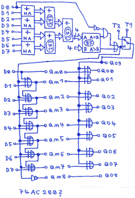
dvi1.png [ 383.45 KiB | Viewed 939 times ]

Attachment:
dvi2.png
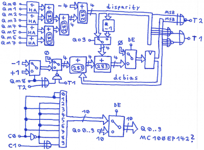
dvi2.png [ 419.3 KiB | Viewed 939 times ]


//Don't get confused: for the intermediade results, I had tried to stick with the DVI specification somehow.

D0..7 is a Byte which sets the color for one channel.
DE is display enable, if DE is LOW we are not in the visible part of the picture.
If DE is LOW, C0 and C1 of the blue channel seem to be the horizontal\vertical sync signals.
For DVI, C0 and C1 for the other two color channels are supposed to be LOW. //For HDMI, it's different.
Q0..9 is the encoder output which feeds the data inputs of a fast 10 Bit shift register.

The adder boxes labeled "HA" are half adders, basically an XOR gate and a AND gate,
sort of a habit when adding partial sums in a multiplier or such...

;---

Of course, my block diagram above never would be able to run at dot clock speed.
One needs to break it into, let's say, a 5 level pipeline and to replace the 7485 comparator and the 74283 adders with something that's much faster.

Serial upstream would be 10 times faster than the dot clock, and at a reasonable dot clock IMHO TTL would be too slow,
this asks for OnSemi PECL shift registers. Microchip\Micrel has neat level translators.

Physically, what goes through the DVI\HDMI cable seems to be CML, Microchip\Micrel has neat CML drivers and flipflops, too.
But IMHO the timing skew between the four channels after the encoders (three color chanels and a dot clock channel) would be critical.

Bad thing is: the block diagram only is one channel, so building a non_proprietary DVI encoder would take a lot of chips.

I would estimate it might take at least half a year to build something like that,
and maybe more than 200€ of material cost... if it works at first try, and it usually doesn't.
//DVI encoder chip might cost just 5€ or such.

Of course, one could be cheating and use fast SRAM (preferably sychronous RAM) as a lookup table (LUT) for replacing that lump of TTL chips,
but then one needs to initialize the lookup table in the RAM from a ROM at power up.

Attachment:
dvi_3.png
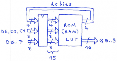
dvi_3.png [ 114.64 KiB | Viewed 939 times ]


I'm happy I got that stuff off my desk, now to let this thread alone for a while.


Top
 Profile  
Reply with quote  
Display posts from previous:  Sort by  
Post new topic Reply to topic  [ 115 posts ]  Go to page Previous  1 ... 4, 5, 6, 7, 8

All times are UTC


Who is online

Users browsing this forum: No registered users and 14 guests


You cannot post new topics in this forum
You cannot reply to topics in this forum
You cannot edit your posts in this forum
You cannot delete your posts in this forum
You cannot post attachments in this forum

Search for:
Jump to: