6502.org Forum  Projects  Code  Documents  Tools  Forum
It is currently Sun Apr 28, 2024 6:37 am

All times are UTC


Post new topic Reply to topic  [ 5 posts ] 
Author Message
PostPosted: Sun Feb 11, 2018 10:48 pm 
Offline
User avatar

Joined: Sun Sep 08, 2013 10:24 am
Posts: 740
Location: A missile silo somewhere under southern England
Hi guys

I'm still working on my 65C02GPD v2 design, having "fun" routing it all atm :lol:.
While looking at the datasheet for the MCP7940N (I2C RTCC which I plan to incorporate) I noticed that it recommends surrounding the 32KHz crystal/can used for timing with a pour which is grounded.
This should encompass the oscillator circuit entirely (see below) and no traces should be run underneath (same layer or any other layer).

Is this something that I should be doing for my main PHI2 source? I tend to have that as a DIL socket-ed can which then runs to a D type flipflop. I.e. should I be doing away with the socket?

I also found some advice which says that if this is done I should put a pour underneath the can on the top layer (this is a layer 4 PCB - middle two layers are GND and VCC) and on the bottom layer, link both to the GND layer then solder the chassis of the can to both pours.
If so, is capacitance an issue here?

Again, is this something that you guys tend to bother with? I assume to avoid noise on the PCB from the crystal/can?

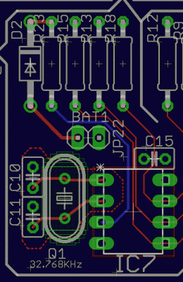
This is what I've done with regards the RTCC so far:
Attachment:
Capture.GIF
Capture.GIF [ 53.18 KiB | Viewed 3024 times ]


IC7 is the MCP7940N
The red dotted somewhat asymmetric area is the top layer pour which is linked to the ground plane via the cathodes of the two capacitors C10 & C11. I haven't yet added a bottom layer one.

Any thoughts/advice welcome :)


Top
 Profile  
Reply with quote  
PostPosted: Mon Feb 12, 2018 4:04 am 
Offline
User avatar

Joined: Fri Aug 30, 2002 1:09 am
Posts: 8428
Location: Southern California
Crystal impedance is very high, in the tens of thousands of ohms, even at its series resonance. What they're trying to prevent is capacitive coupling of other signals into the crystal circuit which could upset the oscillator's operation. Most of digital work is low-impedance; so the greater coupling problem is inductive, with transmission-line effects; but this one might be considered more like audio which is high-impedance and where shielding is for preventing capacitive coupling. In the case of the oscillator can however, it's all self-contained within the can which totally shields it from everything. So you don't need such guard rings if you use the can.

_________________
http://WilsonMinesCo.com/ lots of 6502 resources
The "second front page" is http://wilsonminesco.com/links.html .
What's an additional VIA among friends, anyhow?


Top
 Profile  
Reply with quote  
PostPosted: Mon Feb 12, 2018 5:00 pm 
Offline
User avatar

Joined: Sun Sep 08, 2013 10:24 am
Posts: 740
Location: A missile silo somewhere under southern England
Thanks for advising Garth.
I'm not at all good with analogue electronics (to my own detrimient), but are you saying the following?
So by not routing signals underneath the crystal you're avoiding affecting the crystal from the capacitance in the signal traces? or is the capacitance developed due to have one above the other?
Again, sorry for the lack of understanding.

With regards to using a can: I'd love to, but my PCB is so crowded that I've gone for a standard crystal for now.once I get the rest of the routing done I can see what I squeeze in.
The PCB restriction is down to using a version of EagleCAD which limits me to 160mm x 100mm. Already had to bring the VIA count down from 4 to 3.


Top
 Profile  
Reply with quote  
PostPosted: Mon Feb 12, 2018 8:44 pm 
Offline
User avatar

Joined: Fri Aug 30, 2002 1:09 am
Posts: 8428
Location: Southern California
banedon wrote:
Thanks for advising Garth.
I'm not at all good with analogue electronics (to my own detrimient), but are you saying the following?
So by not routing signals underneath the crystal you're avoiding affecting the crystal from the capacitance in the signal traces? or is the capacitance developed due to have one above the other?

Stray capacitance would couple unwanted signals into the crystal circuit. If those other traces were quiet, ie, had no signal on them, there would be no problem; but the crystal circuit will be far more sensitive to this than your regular digital circuits are. The math behind the design of dependable oscillators of this kind is pretty heavy (S-plane, Laplace transforms, etc.), and I wish I understood it better myself. Further, the effects of parasitic capacitances might be pretty hard to model. But this is why they give rigid guidelines for board layout (so we don't have to understand it all), and why often it's better to just use an oscillator can where everything has been taken care of and it's all shielded in the can and buffered so it's somewhat foolproof. I would think that if you have a true ground plane (not just pours) and you run traces underneath it, on the other side from the crystal circuit, you'd be fine; but I'd rather not have to do a second board just because there was something I overlooked.

Quote:
With regards to using a can: I'd love to, but my PCB is so crowded that I've gone for a standard crystal for now.once I get the rest of the routing done I can see what I squeeze in.

The amount of space you're taking for the crystal, load capacitors, labels for C10, C11, Q1 and its frequency (BTW, crystals are X, so it should be X1; Q is for transistors), and guard ring take approximately the amount of space a half-can oscillator would take anyway. If surface-mount is an option, SMT oscillators can be had in packages considerably smaller than the crystal. On the densest designs I do for work, there's no room for labels, so I leave them off the board. They show up in the CAD, but if we were to actually print the legend on the board, we'd be trying to solder to ink instead of to copper. We have no room for labels between parts.

_________________
http://WilsonMinesCo.com/ lots of 6502 resources
The "second front page" is http://wilsonminesco.com/links.html .
What's an additional VIA among friends, anyhow?


Top
 Profile  
Reply with quote  
PostPosted: Mon Feb 12, 2018 10:36 pm 
Offline
User avatar

Joined: Sun Sep 08, 2013 10:24 am
Posts: 740
Location: A missile silo somewhere under southern England
Good point with regards the space. I made the initial decision at the design stage, but I'll convert it over to a half can as you suggested. Going by the data sheet all I need to do is connect X1 and leave X2 floating. BTW the Q1 actually came from the symbol in Eagle so very odd!

And thanks for the further explanation. I think I understand it now (at least basically). I'll still avoid running any traces beneath the can in any case.

[edit] Here's the new layout:

Attachment:
Capture2.GIF
Capture2.GIF [ 114.19 KiB | Viewed 2944 times ]


Top
 Profile  
Reply with quote  
Display posts from previous:  Sort by  
Post new topic Reply to topic  [ 5 posts ] 

All times are UTC


Who is online

Users browsing this forum: No registered users and 20 guests


You cannot post new topics in this forum
You cannot reply to topics in this forum
You cannot edit your posts in this forum
You cannot delete your posts in this forum
You cannot post attachments in this forum

Search for:
Jump to: