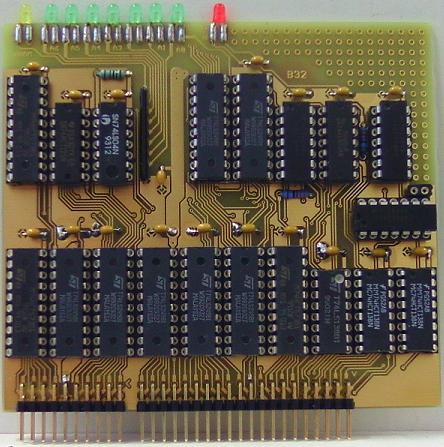
Congratulations: initial PCB Layout looks nice.
Just a thought:
Maybe it would have been better to route the central GND\VCC traces in the middle of the PCB
(going North between U39 and U40) instead of at the left edge of the PCB (U10).
To me, space between the ICs looks good when using small ceramic capacitors,
it's also possible to have the ICs on top of the PCB and the capacitors at the bottom.
(In my projects, I sometimes had placed the capacitors below the IC sockets).
Using SMD capacitors at the bottom of the PCB also might be an idea.
It's an interesting question, if you want to put those ICs into sockets.
If you do, don't save money on the wrong end and buy precision sockets.
(There are precision sockets with capacitor integrated, but I think they would be too expensive.)
BTW: back in 2009, I had two defective TTL chips fresh from the factory.
Would recommend to have 14 pins instead of just 4 pins for the oscillator Y1,
either by changing the package or by creatively adding some vias.
This way, you sould solder a 14 pin precision socket into the PCB,
then plug different oscillators into it for speed testing etc.
Hmm... that button South of Y1 looks like a reset switch, discharging an electrolytic capacitor.
Maybe it would be good to have a resistor between switch and capacitor to limit the current.
If you happen to have enough free space between U10\U11 and the electrolytic capacitor,
you could place a big diode there (anode connected to GND, cathode connected to VCC),
that short_circuits the power supply if it would be reversed by accident.
Maybe SB560... or a TVS diode...
Another trick to prevent the power supply from connected in the wrong way by accident
would be making P1 a three pin screw terminal with VCC in the middle and the other two pins GND.
There seems to be some free space in the South East edge of the PCB,
would suggest to place a "field of vias" there.
If something in the CPU won't work as intended, this would give you a chance
of "bread boarding" a little circuitry with three chips or so for trying to fix it.