6502.org Forum  Projects  Code  Documents  Tools  Forum
It is currently Sat Apr 27, 2024 8:24 pm

All times are UTC


Post new topic Reply to topic  [ 55 posts ]  Go to page 1, 2, 3, 4  Next
Author Message
PostPosted: Wed Dec 07, 2016 9:56 pm 
Offline
User avatar

Joined: Tue Oct 25, 2016 8:56 pm
Posts: 360
Well, I promised ttlworks that I'd post this, so here it is in all its glory. This is the complete schematic for the mainboard of my first 6502-based-computer, which doubles as a testbed for the FPGA-version that I'm making for my uni project.

Features:
  • 3.3V throughout (necessary for compatibility with the FPGA chip)
  • 16KiB RAM
  • 32KiB ROM Cartridge
  • 8KiB Internal BIOS/OS ROM
  • Selectable 1MHz, 2MHz or External clock
  • Single-Instruction stepping
  • 3x SPI-10 (3.3V Variant) headers
  • GPIO Header (intended to interface with Daryl Richtor's Video Chip but will work perfectly well as arbitrary I/O)
  • Serial I/O Expansion Port (based on Garth Wilson's Math EEPROM interfacing circuit)
  • Full RS-232 port, using SC16C550 and MAX3241. Originally I was going to use WDC's ACIA, but it doesn't work with 3.3V and that transmit bug is insidious.
  • VHDC Connector to interface with FPGA. Computer can operated with either a "real" 65C02, or my FPGA recreation via the VHDC connector.
  • Test points. Test points everywhere!

If anyone has any comments / concerns / musings, I am extremely open to hear them. I appreciate you've probably seen all this stuff before, but its new to me.


Attachments:
File comment: FPGA-6502 Test Computer Mainboard Schematic, rev 5.
FPGA-6502-schematic-rev5.png
FPGA-6502-schematic-rev5.png [ 224.52 KiB | Viewed 2238 times ]

_________________
Want to design a PCB for your project? I strongly recommend KiCad. Its free, its multiplatform, and its easy to learn!
Also, I maintain KiCad libraries of Retro Computing and Arduino components you might find useful.
Top
 Profile  
Reply with quote  
PostPosted: Thu Dec 08, 2016 8:44 am 
Offline
User avatar

Joined: Fri Nov 09, 2012 5:54 pm
Posts: 1392
Hi, Alarm Siren, and thanks for posting the schematics.
Now for my two cents:

I'm not sure, if you really going to need those 22k pulldown resistors on the data bus.

Maybe inserting a jumper between the /NMI output of the single_stepping circuitry
and the /NMI input of the CPU would be a good idea: if you would be going to need
/NMI for some peripheral later, this would make it possible to "improvise" something.

16kB of RAM ain't much, in the long run you might be better off with 32kB.
For instance, displaying 320*200 monochrome graphics instantly will eat up 8000 Bytes of memory.

From the schematics, I'd say the board will contain 8kB ROM (that's OK),
but to me the part number of the ROM chip looks a bit exotic...
are you sure that it is available ?

Microchip has some neat flash ROMs with parallel interface:
http://www.microchip.com/ParamChartSearch/chart.aspx?branchID=71301&mid=&lang=en

Another alternative would be Atmel:
http://www.atmel.com/products/memories/eprom/default.aspx
IMHO it would be OK to have just a boot loader in OTP ROM on the CPU PCB which then
loads code (including the operating system) from an external serial flash ROM...
since you already are out to use a 6522 for implementing a SPI interface.

16C550 could be a little bit sensitive to timing problems when adding it to a 6502 bus,
take care there.

Maybe placing 100 Ohm resistors between the MAX level converter and the 9 pin DSUB connector
might be a good idea just in case something goes wrong when plugging the SBC to a PC. ;)
To prevent the SBC from "accidentally getting confused" by ESD discharge,
it also might be a good diea to have 100 Ohm between the RS232 cable shield and GND of the SBC.

The 16C550 and the 6522 have more than one chip select input,
maybe you could throw out one of the 74138s in the address decoder
when making "creative use" of the unused chip select inputs.

Don't have any experience with the DS1818 reset chip,
the question is how sensitive it is to spikes in the power supply.
Maybe it would be a good idea to have a 10 Ohms resistor between the 3.3V power supply
and the DS1818 3.3V input... plus another capacitor in parallel to C11
(there are neat 10uF ceramic capacitors available in 1206 package).
It's nice, that the DS1818 internally has a 5.5 kOhm pullup at the /RES output.

I'd suggest adding a TVS protection diode to the power supply,
so an ESD discharge or a "reversed" power supply would do less damage.
(One trick to prevent the power supply from getting reversed "by accident"
is using a three pin connector where pin 1 and pin 3 are GND).

Also, I'd suggest to build the clock generation a little bit different.
You are using a 7474 as frequency divider (two counters 1 Bit each).
74393 has the same amount of pins as the 7474, but contains two counters 4 Bit each.
This would give you more flexibility when choosing the crystals\oscillators.
For instance, a 16MHz oscillator might be less expensive and better available
than a 4MHz oscillator... it's just a thought.
When building my own 6502 SBC, the clock generation looked like this:

Attachment:
drc2_clk.png
drc2_clk.png [ 19.61 KiB | Viewed 2216 times ]


Oh, and I'd like to point out that there are different approaches to generating a video signal.
For instance, my CRT\LCD controller passively snooped the 6502 bus for write cycles
and mirrored them into its own RAM, so CPU and CRT controller can run from different
clock sources\frequencies...

But for a first try, your schematic look nice, and you sure had spent some time
with digging through the info available around here.
:)

Good luck with your project, looking forward to watching your progress.


Top
 Profile  
Reply with quote  
PostPosted: Thu Dec 08, 2016 9:16 am 
Offline
User avatar

Joined: Tue Oct 25, 2016 8:56 pm
Posts: 360
ttlworks wrote:
Hi, Alarm Siren, and thanks for posting the schematics.
Now for my two cents:

I'm not sure, if you really going to need those 22k pulldown resistors on the data bus.


I put them in so if I attempt to access a non-existent device (ROM Cart not plugged in, non-implemented I/O device, etc) I'll get a known value (0). I wasn't sure, and could find no information on, whether the Data bus pins on the 65c02 has internal pull resistors for this purpose or no.

Quote:
Maybe inserting a jumper between the /NMI output of the single_stepping circuitry
and the /NMI input of the CPU would be a good idea: if you would be going to need
/NMI for some peripheral later, this would make it possible to "improvise" something.

That is a very good point, and something I actually intended to do and forgot!

Quote:
16kB of RAM ain't much, in the long run you might be better off with 32kB.
For instance, displaying 320*200 monochrome graphics instantly will eat up 8000 Bytes of memory.

Fair point and not one I'd given much thought to, but equally I'm not expecting this design to directly drive graphics. If it outputs to a monitor at all, it'll be via the RS-232 or one of Daryl Richtor's Text Video boards. I shall bear this in mind for the future, non-uni-project version though.

Quote:
From the schematics, I'd say the board will contain 8kB ROM (that's OK),
but to me the part number of the ROM chip looks a bit exotic...
are you sure that it is available ?

Absolutely. I got the delivery a couple of days ago. Its just the 3.3V version of the AT28C64B.


Quote:
Microchip has some neat flash ROMs with parallel interface:
http://www.microchip.com/ParamChartSearch/chart.aspx?branchID=71301&mid=&lang=en

Trying to avoid flash-proper because of the page-write thing. Not an issue for the BIOS chip, I suppose, but I'm using the same chips in the Program Cartridge, and I'd like for it to be possible (at least in principle) for the SBC to write to its own ROM, with a minimum of complexity. I've not put up the schematics for that, but the four chips on the Cart have jumpers to allow/deny writing to them individually.

Quote:
Another alternative would be Atmel:
http://www.atmel.com/products/memories/eprom/default.aspx
IMHO it would be OK to have just a boot loader in OTP ROM on the CPU PCB which then
loads code (including the operating system) from an external serial flash ROM...
since you already are out to use a 6522 for implementing a SPI interface.

For now, One-Time-Programmable is definitely off the table, even for the BIOS: this thing is going to be buggy as hell initially. My programs always are :P . I shall bear in mind this way of doing things (that is, bootloader on board, big ram, main ROM on SPI) for the future though. It definitely sounds like it has merits to me.

Quote:
16C550 could be a little bit sensitive to timing problems when adding it to a 6502 bus,
take care there.

Can you be more specific? The pin descriptions and timing diagram suggest to me it should be fully compatible...

Quote:
Maybe placing 100 Ohm resistors between the MAX level converter and the 9 pin DSUB connector
might be a good idea just in case something goes wrong when plugging the SBC to a PC. ;)
To prevent the SBC from "accidentally getting confused" by ESD discharge,
it also might be a good diea to have 100 Ohm between the RS232 cable shield and GND of the SBC.

Fair points; means I have to edit both the schematic symbol and the footprint of the DE9. What fun. Wouldn't the resistors interfere with the voltages though? The transceiver is already (from my understanding) only capable of driving up to +/-5.5V, which is pretty close to the RS-232 no-go-zone.

Quote:
The 16C550 and the 6522 have more than one chip select input,
maybe you could throw out one of the 74138s in the address decoder
when making "creative use" of the unused chip select inputs.

I did exactly that in an earlier revision, my supervisor suggested I not do it that way.

Quote:
Don't have any experience with the DS1818 reset chip,
the question is how sensitive it is to spikes in the power supply.
Maybe it would be a good idea to have a 10 Ohms resistor between the 3.3V power supply
and the DS1818 3.3V input... plus another capacitor in parallel to C11
(there are neat 10uF ceramic capacitors available in 1206 package).
It's nice, that the DS1818 internally has a 5.5 kOhm pullup at the /RES output.

There are three sensitivities available: 5%, 10% and 15%. I have ordered the 5% one. I get what the extra cap would do, but what would the resistor achieve?

Quote:
I'd suggest adding a TVS protection diode to the power supply,
so an ESD discharge or a "reversed" power supply would do less damage.
(One trick to prevent the power supply from getting reversed "by accident"
is using a three pin connector where pin 1 and pin 3 are GND).

In most circumstances (and certainly once I've finished developing everything), the SBC will be powered from the FPGA board via the VHDC connector. The screw terminal is so I can power it from a bench power supply during development, when I've put in the "real" 65c02 instead of the FPGA. As such, I don't envisage it being a particular issue. Nevertheless, it can't hurt to throw in a clamping diode. Any suggestions for specific part?

Quote:
Also, I'd suggest to build the clock generation a little bit different.
You are using a 7474 as frequency divider (two counters 1 Bit each).
74393 has the same amount of pins as the 7474, but contains two counters 4 Bit each.
This would give you more flexibility when choosing the crystals\oscillators.
For instance, a 16MHz oscillator might be less expensive and better available
than a 4MHz oscillator... it's just a thought.
When building my own 6502 SBC, the clock generation looked like this:

Attachment:
drc2_clk.png


Fair enough. I'll look at that for the non-project versions, but for now the 4MHz Oscillator etc have already arrived.

Quote:
Oh, and I'd like to point out that there are different approaches to generating a video signal.
For instance, my CRT\LCD controller passively snooped the 6502 bus for write cycles
and mirrored them into its own RAM, so CPU and CRT controller can run from different
clock sources\frequencies...

Good knowledge, though I'm not intending to have this SBC directly drive a monitor. If it does so, it'll be via the RS-232 or one of Daryl Richtor's Text Video peripheral boards.

Quote:
But for a first try, your schematic look nice, and you sure had spent some time
with digging through the info available around here.
:)

Good luck with your project, looking forward to watching your progress.

Thank you, and I am extremely grateful for your input.

_________________
Want to design a PCB for your project? I strongly recommend KiCad. Its free, its multiplatform, and its easy to learn!
Also, I maintain KiCad libraries of Retro Computing and Arduino components you might find useful.


Top
 Profile  
Reply with quote  
PostPosted: Thu Dec 08, 2016 10:05 am 
Offline
User avatar

Joined: Fri Nov 09, 2012 5:54 pm
Posts: 1392
Quote:
[22k pulldown resistors > data bus]
I put them in so if I attempt to access a non-existent device (ROM Cart not plugged in, non-implemented I/O
device, etc) I'll get a known value (0). I wasn't sure, and could find no information on, whether the Data bus
pins on the 65c02 has internal pull resistors for this purpose or no.

I don't think that the 65C02 data bus pins have internal pull resistors.
Having a known value on the data bus in case of having an "open" data bus makes sense.

Quote:
[16kB RAM]
Fair point and not one I'd given much thought to, but equally I'm not expecting this design to directly
drive graphics. If it outputs to a monitor at all, it'll be via the RS-232 or one of Daryl Richtor's
Text Video boards. I shall bear this in mind for the future, non-uni-project version though.

So it's only text mode (for debugging), and this text mode doesn't have to be fast.
BTW: there might be text LCDs with SPI.

Quote:
Trying to avoid flash-proper because of the page-write thing. Not an issue for the BIOS chip,
I suppose, but I'm using the same chips in the Program Cartridge, and I'd like for it to be possible
(at least in principle) for the SBC to write to its own ROM, with a minimum of complexity.
I've not put up the schematics for that, but the four chips on the Cart have jumpers to
allow/deny writing to them individually.

Write protect, nice idea.
It is true that the page layout of flash memory chips might vary a little bit... :)

Quote:
For now, One-Time-Programmable is definitely off the table, even for the BIOS: this thing is going to be
buggy as hell initially. My programs always are :P . I shall bear in mind this way of doing things
(that is, bootloader on board, big ram, main ROM on SPI) for the future though.
It definitely sounds like it has merits to me.

Well, if OTP ROM _only_ would contain a boot loader, one could focus on making a bug free boot loader,
and the rest of the software which would be going to be loaded into RAM could stay as buggy as hell. ;)
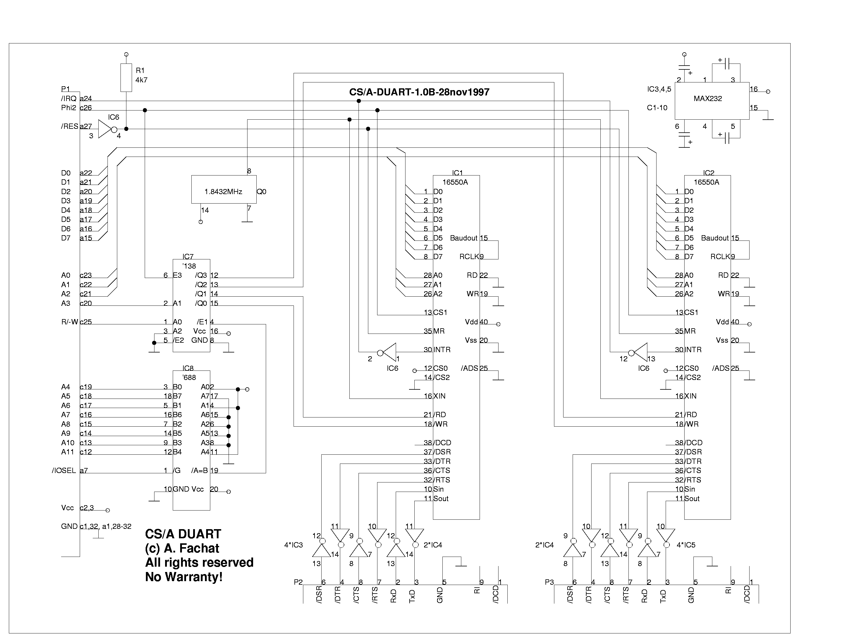
Quote:
[16C550]
Can you be more specific? The pin descriptions and timing diagram suggest to me it should be fully compatible...

Hmm... I now have to admit that I haven't used the 16C550 together with a 6502.
But I remember to have had some timing problems back in 2000, when using a chip similar to the 16C550
together with a Shark (ADSP21065L). So I made this remark just out of a "gut feeling".

Anyhow, using non_6502 related peripheral chips on a 6502 bus could provide more trouble
than using 6502 related peripherals on a 6502 bus...

Quote:
Fair points; means I have to edit both the schematic symbol and the footprint of the DE9.
What fun. Wouldn't the resistors interfere with the voltages though? The transceiver is already
(from my understanding) only capable of driving up to +/-5.5V, which is pretty close to the RS-232
no-go-zone.

I'm not familiar with the MAX level converter you are going to use,
but I had used 100 Ohm resistors together with a MAX3232.

Depends on the current that is going to flow through the resistors,
if you are paranoid just change 100Ohm to 22Ohm.

Quote:
The 16C550 and the 6522 have more than one chip select input,
maybe you could throw out one of the 74138s in the address decoder
when making "creative use" of the unused chip select inputs.
Quote:
I did exactly that in an earlier revision, my supervisor suggested I not do it that way.

Sorry to hear, that it's a political thing. !

Quote:
There are three sensitivities available: 5%, 10% and 15%. I have ordered the 5% one.
I get what the extra cap would do, but what would the resistor achieve?

The resistor and the extra cap would build up a low_pass filter for the 3.3V supply of the DS1818.
I had used TL7705 for generating /RES, and that chip has quite a reputation to being a bit
sensitive to "dirt" in the power supply. :)

Quote:
In most circumstances (and certainly once I've finished developing everything),
the SBC will be powered from the FPGA board via the VHDC connector.
The screw terminal is so I can power it from a bench power supply during development,
when I've put in the "real" 65c02 instead of the FPGA. As such, I don't envisage it
being a particular issue. Nevertheless, it can't hurt to throw in a clamping diode.

Ja, so when some of the mechatronics students had toyed with their little robot
here at the university, they accidentally had reversed the power supply
shortly before the project deadline... what meant replacing plenty of chips... ;)

Quote:
[74393 clock generator]
Fair enough. I'll look at that for the non-project versions, but for now the 4MHz Oscillator etc
have already arrived.

Yep, you got to go with what's there, then with what's available. :)

Quote:
Good knowledge, though I'm not intending to have this SBC directly drive a monitor.
If it does so, it'll be via the RS-232 or one of Daryl Richtor's Text Video peripheral boards.

That's OK, just be sure that the computer still works when no video display is installed...

Quote:
Good luck with your project, looking forward to watching your progress.
Quote:
Thank you, and I am extremely grateful for your input.

You are welcome, and we always like to see a new 6502 project here in the forum.


Top
 Profile  
Reply with quote  
PostPosted: Thu Dec 08, 2016 3:09 pm 
Offline
User avatar

Joined: Fri Dec 11, 2009 3:50 pm
Posts: 3346
Location: Ontario, Canada
Hi, guys. Dieter has put in his two cents worth, and now I will make some comments as well. Probably mine will work out to just a fraction of a penny!

What value do you see in arranging for the data bus to read a predictable value (such as $00 or $FF) when no device is driving the bus? (Hmm, $00 is BRK, so to some extent you could catch runaway code that way.) In any case if pullup or pulldown resistors are used to accomplish this then there'll be an RC delay to consider, based on the resistance of the resistors and the capacitance of the data bus lines. Unless the clock rate is reduced you'll probably need resistors much smaller than 22K if the scheme is to work reliably -- and smaller resistors increase the loading seen by the various devices driving the bus.

(FWIW, in the case of an explicit test there's an alternative way of detecting an undriven bus, and that is to look for the value of the last instruction byte. Example: if you want to test whether there's any device at $1234, code a LDA $1234. When this executes, the data bus will have $AD, $34, $12 during the three cycles when the instruction is fetched. The actual data fetch occurs in the fourth cycle. If no device is present then the $12 will still be there, stored by the bus's capacitance. :) There are some caveats, but I'll cut this short unless someone wants further detail.)

Quote:
The 16C550 and the 6522 have more than one chip select input,
maybe you could throw out one of the 74138s in the address decoder
when making "creative use" of the unused chip select inputs.
Quote:
I did exactly that in an earlier revision, my supervisor suggested I not do it that way.
There's a tradeoff here. Using the additional chip select inputs has potential to save some hardware and thus reduce manufacturing cost. For a commercial product this is probably the best choice. But, during debug, it's harder to tell when the device is being accessed. If just a single chip select is used then it can very quickly be examined via oscilloscope.

best of luck, Alarm Siren -- have fun!

Jeff

_________________
In 1988 my 65C02 got six new registers and 44 new full-speed instructions!
https://laughtonelectronics.com/Arcana/ ... mmary.html


Top
 Profile  
Reply with quote  
PostPosted: Thu Dec 08, 2016 8:25 pm 
Offline
User avatar

Joined: Fri Aug 30, 2002 1:09 am
Posts: 8428
Location: Southern California
Alarm Siren wrote:
ttlworks wrote:
Maybe placing 100 Ohm resistors between the MAX level converter and the 9 pin DSUB connector
might be a good idea just in case something goes wrong when plugging the SBC to a PC. ;)
To prevent the SBC from "accidentally getting confused" by ESD discharge,
it also might be a good diea to have 100 Ohm between the RS232 cable shield and GND of the SBC.

Fair points; means I have to edit both the schematic symbol and the footprint of the DE9. What fun. Wouldn't the resistors interfere with the voltages though? The transceiver is already (from my understanding) only capable of driving up to +/-5.5V, which is pretty close to the RS-232 no-go-zone.

The MAX3246E is already ESD-protected for 9KV contact, 15KV human-body model, and in that case 22Ω or 100Ω isn't really going to do anything. In more than 25 years of working with this stuff, the only related problem I've had was the rare latch-up on a Rockwell 65c22 interfaced directly to the parallel printer on a different mains circuit across the room, and the problem did not happen when connecting, but after it was connected, and there was some kind of spike on the mains. The processor did not "get confused," but the VIA latched up and got hot.

Quote:
Quote:
The 16C550 and the 6522 have more than one chip select input,
maybe you could throw out one of the 74138s in the address decoder
when making "creative use" of the unused chip select inputs.

I did exactly that in an earlier revision, my supervisor suggested I not do it that way.

Tell your supervisor that that's what they're there for, and that two 74HC138's cascaded could have 100ns propagation delay @ 3.3V (increasing to 400ns @ 2V). What was he thinking??

Quote:
I'm not intending to have this SBC directly drive a monitor. If it does so, it'll be via the RS-232 or one of Daryl Richtor's Text Video peripheral boards.

Cool!

Jeff is right about the bus capacitance and the pull-down resistor values. 22K times let's guess 30pF is a time constant of 660ns, a little too long even at 1MHz. A TC is how long it takes to traverse 1-1/e of the way from one steady-state voltage to the other; so for example if going from 0 to 3.3V (being generous to say the driver can pull all the way to the rails under the expected conditions), a TC will get you up to 3.3V*.632=2.086V; or going down, down to 1.214V. That's not even reaching the minimum 70% and 30% thresholds given in the 65c02's data sheet for inputs, let alone reaching them in time to meet set-up times; so you'll want to do better.

I also just noticed the SPI-10 ports. Again, cool!! :D

_________________
http://WilsonMinesCo.com/ lots of 6502 resources
The "second front page" is http://wilsonminesco.com/links.html .
What's an additional VIA among friends, anyhow?


Top
 Profile  
Reply with quote  
PostPosted: Fri Dec 09, 2016 8:47 am 
Offline
User avatar

Joined: Fri Nov 09, 2012 5:54 pm
Posts: 1392
Took a look at the MAX3241E datasheet.
It's a nice chip, and I think you don't need resistors between the MAX and the 9 pin DSUB.
BTW: the datasheet says, that 100nF capacitors would do for the charge pump.

;---

Back in 1997, fachat did use 16550A on a 6502 bus.

From the part number, the UART you are going to use is the NXP SC16C550BIB48. //LQFP48
And the CPU is a W65C02S6TPG-14. //PDIP40

The timing of those new chips might be a bit different from the old chips fachat had used back then.

W65C02 has >10ns hold time after the falling edge of "PHI2" for address (tAH) and write data (tDHW).
Be warned, that the signal labeled 'PHI2' in the timing diagram of the WDC datasheet
actually is the clock input of the CPU, means pin 37 (not the PHI2 output at pin 39).
The WDC datasheet does not specify the delay from clock input to PHI2 output !

Would recommend to tie pin 1 of U1A and pin 5 of U1B to pin 37 of the CPU instead.

Edit: I also would recommend to tie the 6522 clock input to the CPU clock input.

SSC16C550 with /AS tied to GND:
/IOR,/IOW rising edge hold time for address: t7h' >5ns
/IOW rising edge hold time for data: t16h >5ns

Hmm.
NXP 74HC00 datasheet doesn't specify the propagation delay at 3.3V supply voltage.
25ns typ for 2.0V, 9ns typ. for 4.5V.
So let's just assume ca. 17ns typ. for 3.3V and 25 Celsius.

;---

This means that the rising edge at /RE (/IOR) and /WE (IOW) would occur maybe 17ns after the falling edge
of the clock input of the CPU.

The CPU might hold address and write data for 10ns on the bus after the falling edge
of the input clock of the CPU.

SC16C550 would like to have write data and address stable for 5nS after the rising edge of /RE and /WE.
...but in the worst case scenario, and when ignoring bus capacitance, write data and address on the bus
might be getting unstable 12ns before this point.

Alsi: please check/re_calculate your timing to prove me wrong. :)

BTW: 74LVC00 is a little bit faster than 74HC00.


Top
 Profile  
Reply with quote  
PostPosted: Fri Dec 09, 2016 11:42 am 
Offline
User avatar

Joined: Tue Oct 25, 2016 8:56 pm
Posts: 360
Dr Jefyll wrote:
What value do you see in arranging for the data bus to read a predictable value (such as $00 or $FF) when no device is driving the bus? (Hmm, $00 is BRK, so to some extent you could catch runaway code that way.) In any case if pullup or pulldown resistors are used to accomplish this then there'll be an RC delay to consider, based on the resistance of the resistors and the capacitance of the data bus lines. Unless the clock rate is reduced you'll probably need resistors much smaller than 22K if the scheme is to work reliably -- and smaller resistors increase the loading seen by the various devices driving the bus.

(FWIW, in the case of an explicit test there's an alternative way of detecting an undriven bus, and that is to look for the value of the last instruction byte. Example: if you want to test whether there's any device at $1234, code a LDA $1234. When this executes, the data bus will have $AD, $34, $12 during the three cycles when the instruction is fetched. The actual data fetch occurs in the fourth cycle. If no device is present then the $12 will still be there, stored by the bus's capacitance. :) There are some caveats, but I'll cut this short unless someone wants further detail.)

The idea was to be able to detect the presence or absence of hardware, e.g. the ROM Cart is user removable, it would make sense for the onboard OS to detect the presence of the Cart before passing control to it. The bus loading issue was why I gave them a high resistance value, but as you rightly point out, they're not actually going to help at these speeds. I had not considered the bus capacitance method for detecting missing hardware; makes sense. I'm going to ditch the resistors and use that method instead, therefore I'm very much interested in hearing the caveats. All this AC stuff makes my head spin :P.

GARTHWILSON wrote:
The MAX3246E is already ESD-protected for 9KV contact, 15KV human-body model, and in that case 22Ω or 100Ω isn't really going to do anything. In more than 25 years of working with this stuff, the only related problem I've had was the rare latch-up on a Rockwell 65c22 interfaced directly to the parallel printer on a different mains circuit across the room, and the problem did not happen when connecting, but after it was connected, and there was some kind of spike on the mains. The processor did not "get confused," but the VIA latched up and got hot.

Yep, the ESD protection was one of my reasons for picking this specific version of the UART.

GARTHWILSON wrote:
Quote:
Quote:
The 16C550 and the 6522 have more than one chip select input,
maybe you could throw out one of the 74138s in the address decoder
when making "creative use" of the unused chip select inputs.

I did exactly that in an earlier revision, my supervisor suggested I not do it that way.

Tell your supervisor that that's what they're there for, and that two 74HC138's cascaded could have 100ns propagation delay @ 3.3V (increasing to 400ns @ 2V). What was he thinking??

I am acutely aware of the timing issues surrounding the '138s. That's one of the reasons I've got 1/2MHz selectable clock, just in case my maths has failed me! However, I don't think the issue will be with the peripherals in terms of address time, but rather with the EEPROMs, which require 200ns from address valid to data access. add 50ns for the '138, and one is cutting it mighty close.

As to my supervisor, his reasoning was threefold: firstly what Jefyll said about being able to determine which peripheral is being accessed easier, secondly no potential danger of bus contention from using a squiffy address and thirdly it would be easier to expand the design in future to include more peripheral devices without re-engineering/coding lots of stuff.

GARTHWILSON wrote:
I also just noticed the SPI-10 ports. Again, cool!! :D

Yep, I think I might well be one of the first computers to implement them! An earlier revision used the 65SIB, but SPI-10 just seemed easier to me, and saved me from needing a bunch of extra voltages.

ttlworks wrote:
Took a look at the MAX3241E datasheet.
It's a nice chip, and I think you don't need resistors between the MAX and the 9 pin DSUB.
BTW: the datasheet says, that 100nF capacitors would do for the charge pump.

Yep, but it also says that using larger capacitors reduces ripple and increases efficiency. It also warns about capacitor aging when using the minimum requirements. This just seemed like a better plan.

ttlworks wrote:
Back in 1997, fachat did use 16550A on a 6502 bus.

From the part number, the UART you are going to use is the NXP SC16C550BIB48. //LQFP48
And the CPU is a W65C02S6TPG-14. //PDIP40

The timing of those new chips might be a bit different from the old chips fachat had used back then.

W65C02 has >10ns hold time after the falling edge of "PHI2" for address (tAH) and write data (tDHW).
Be warned, that the signal labeled 'PHI2' in the timing diagram of the WDC datasheet
actually is the clock input of the CPU, means pin 37 (not the PHI2 output at pin 39).
The WDC datasheet does not specify the delay from clock input to PHI2 output !

Would recommend to tie pin 1 of U1A and pin 5 of U1B to pin 37 of the CPU instead.

Edit: I also would recommend to tie the 6522 clock input to the CPU clock input.

SSC16C550 with /AS tied to GND:
/IOR,/IOW rising edge hold time for address: t7h' >5ns
/IOW rising edge hold time for data: t16h >5ns

Hmm.
NXP 74HC00 datasheet doesn't specify the propagation delay at 3.3V supply voltage.
25ns typ for 2.0V, 9ns typ. for 4.5V.
So let's just assume ca. 17ns typ. for 3.3V and 25 Celsius.

;---

This means that the rising edge at /RE (/IOR) and /WE (IOW) would occur maybe 17ns after the falling edge
of the clock input of the CPU.

The CPU might hold address and write data for 10ns on the bus after the falling edge
of the input clock of the CPU.

SC16C550 would like to have write data and address stable for 5nS after the rising edge of /RE and /WE.
...but in the worst case scenario, and when ignoring bus capacitance, write data and address on the bus
might be getting unstable 12ns before this point.

Alsi: please check/re_calculate your timing to prove me wrong. :)

BTW: 74LVC00 is a little bit faster than 74HC00.


Yes, those are the chips I'm using. I'm afraid I can't prove you wrong, as you appear to be right, and its not something I'd considered at all. It looks to me like its going to be an issue on the RAM/ROM too; their hold times are 0ns, but that still means they expect to see the valid address at the positive edge of !WE, which they might not as the address potentially started changing 17ns - 10ns = 7ns ago.

I was not familiar with the LVC series; the only faster version of the 74 seris I knew about was AHC, which I'd read in various places was well-known for tripping people up for some reason that was never fully explained, so I avoided it. Having said that, LVC does indeed look awesome in terms of prop time - the LVC138 has a prop time worst case of 5.8ns @3.3V, which is obviously amazingly better than the HC138's ~50ns. In other words it looks like switching to LVC will solve most of my timing issues, real or potential. Which is a shame since I've already ordered and received all the 'HC parts, but hey-ho. I don't think I need to replace all the chips - the '74s I don't think are doing anything sufficiently time sensitive as to require the greater speed, but the '138s, '02 and '00 will benefit from a speed increase.

Are there likely to be any pitfalls in using LVC?

_________________
Want to design a PCB for your project? I strongly recommend KiCad. Its free, its multiplatform, and its easy to learn!
Also, I maintain KiCad libraries of Retro Computing and Arduino components you might find useful.


Top
 Profile  
Reply with quote  
PostPosted: Fri Dec 09, 2016 1:58 pm 
Offline
User avatar

Joined: Fri Nov 09, 2012 5:54 pm
Posts: 1392
Alarm Siren wrote:
The idea was to be able to detect the presence or absence of hardware, e.g. the ROM Cart is user removable...

Ah... starting to remember that 68k game with /DTACK and /BERR.
To complete a bus cycle, the addressed hardware had to pull /DTACK low (7405 or 74125) when ready.
If /DTACK wasn't pulled low within some time, a 74393 counter could be used to trigger /BERR (bus error).

For your application, one idea would be to have a /DTACK signal line with a pullup resistor (470 Ohm ?).
The selected hardware has to pull /DTACK low when addressed.
If /DTACK isn't low at the falling edge of PHI2, this triggers a /NMI for entering the monitor program or such...

But if you would be going for pulldown resistors on the data bus, one idea would be to have them resistors
as a 9 pin SIL resistor network, and to plug it into a precision socket so you could experiment with
different resistor values if neccessary.

Alarm Siren wrote:
[MAX3241E]Yep, but it also says that using larger capacitors reduces ripple and increases efficiency.
It also warns about capacitor aging when using the minimum requirements. This just seemed like a better plan.

Yep. Just felt a need to mention this because as a hobbyist one tends to have a bag of 100nF capacitors in the drawer.

Alarm Siren wrote:
Are there likely to be any pitfalls in using LVC?

We are using 3.3V 74LVC245 as 5V\3.3V level translator for SPI interfaces at work since quite a few years.
Works nice, even with some meters of cable at the interface at 2MBit.

Don't have any practical experience with 74AHC, only with 74AC:
IMHO the problem with 74AC is the high energy within the fast rise\fall times of the 74AC outputs.
74AC is supposed to drive low impedances (impedance matched transmission lines etc.),
so in a normal "high impedance" application with relatively long signal lines 74AC could generate
some noise and ringing or such.
Maybe AHC gives you similar trouble.

BTW: Nice, that we catched those timing problems in time. :)


Top
 Profile  
Reply with quote  
PostPosted: Fri Dec 09, 2016 5:08 pm 
Offline
User avatar

Joined: Fri Dec 11, 2009 3:50 pm
Posts: 3346
Location: Ontario, Canada
Alarm Siren wrote:
the only faster version of the 74 seris I knew about was AHC, which I'd read in various places was well-known for tripping people up for some reason that was never fully explained, so I avoided it.
Is it possible you're confusing AC and AHC? Both have fast propagation times. But, as ttlworks explained, the outputs of AC series chips also have very fast rise and fall times, which in many circumstances will provoke ringing unless measures are taken. AHC avoids the fast rise and fall times, but is still fast, propagation-wise (about 3 times as fast as HC, according to some TI doc I read recently).

Quote:
What value do you see in arranging for the data bus to read a predictable value (such as $00 or $FF) when no device is driving the bus?
Quote:
The idea was to be able to detect the presence or absence of hardware, e.g. the ROM Cart is user removable, it would make sense for the onboard OS to detect the presence of the Cart before passing control to it.
Look before you leap, eh? :P

IIRC, BIOS ROM's on removable PC cards manage this by turning the problem around. IOW, the CPU tries to establish that a device *is* connected, rather than establishing that one is not. The first 2 bytes of the ROM contain a prearranged signature value such as $55AA, and if we don't see this then it's no go. (The actual code begins after the signature.) Of course the signature value is chosen to be one that's unlikely to result from an open bus. And it's significant that this scheme uses more than just one byte.

I wrote:
Example: if you want to test whether there's any device at $1234, code a LDA $1234. When this executes, the data bus will have $AD, $34, $12 during the three cycles when the instruction is fetched. The actual data fetch occurs in the fourth cycle. If no device is present then the $12 will still be there, stored by the bus's capacitance.
Assuming your removable cart includes a ROM (and not just some I/O) then maybe there's no advantage to doing it this way (ie; establishing the bus is NOT driven). But FWIW the caveats include the need for caution regarding DC loading that would bleed off the value stored in the data bus capacitance. That won't be an issue if only NMOS or CMOS devices attach to the data bus, but LS or TTL could spell trouble. Also, the example would fail if the device *was* present but happened to read $12. This can be remedied by verifying with a second read of $1234 -- but this time we use different instructions to access that same address. For example, load X with $FF then do a LDA $1135,X. Now the last instruction byte is $11. (This second-read verify won't work with NMOS 6502 because indexed addressing has different bus behavior than 65C02.)

It's a goofy sort of challenge... but fun! :)

-- Jeff

_________________
In 1988 my 65C02 got six new registers and 44 new full-speed instructions!
https://laughtonelectronics.com/Arcana/ ... mmary.html


Top
 Profile  
Reply with quote  
PostPosted: Fri Dec 09, 2016 7:44 pm 
Offline
User avatar

Joined: Fri Aug 30, 2002 1:09 am
Posts: 8428
Location: Southern California
Alarm Siren wrote:
GARTHWILSON wrote:
I also just noticed the SPI-10 ports. Again, cool!! :D

Yep, I think I might well be one of the first computers to implement them! An earlier revision used the 65SIB, but SPI-10 just seemed easier to me, and saved me from needing a bunch of extra voltages.

They're for different things, so my next computer will have both. The SPI-10's will mainly be for tiny modules that plug in to the board, usually having only one IC, similar to the SD (or microSD) card idea, whereas the 65SIB is for larger devices out on a ribbon cable. The latter would be more like workbench instrumentation, things that have many ICs, may have coax cables plugged into them (which is impractical for an SPI-10 module), need more space for connectors and for user interface like maybe needing its own display and keypad and switches, etc..

Quote:
ttlworks wrote:
Took a look at the MAX3241E datasheet.
It's a nice chip, and I think you don't need resistors between the MAX and the 9 pin DSUB.
BTW: the datasheet says, that 100nF capacitors would do for the charge pump.

Yep, but it also says that using larger capacitors reduces ripple and increases efficiency. It also warns about capacitor aging when using the minimum requirements. This just seemed like a better plan.

I have not read anything about MLCCs losing capacitance as they age; but do be aware that their capacitance decreases—a lot—if the voltage across them becomes more than about 20% of WVDC. That's for X7R's which are way better than anything with a "5" in it (Z5U, etc.). The 5's are a lot worse. This is especially critical for minimizing audio distortion in my analog designs for work, so it a capacitor may be charged to as much as 10V in the peaks (which would only happen at the lowest frequencies), I always use 50V capacitors.

I do plan to use 74LVC in my next computer. Jeff got me turned on to those. If there's anything to look out for, or anything even better, I will be interested. There are a lot of single-gate options (like 74LVC1G00) that make board layout easier for some things, and also of course if you only need one gate of the particular type and don't want to take the space of a standard package of four or however many it has. Speeds are outstanding too.

_________________
http://WilsonMinesCo.com/ lots of 6502 resources
The "second front page" is http://wilsonminesco.com/links.html .
What's an additional VIA among friends, anyhow?


Top
 Profile  
Reply with quote  
PostPosted: Fri Dec 09, 2016 10:19 pm 
Offline
User avatar

Joined: Fri Dec 11, 2009 3:50 pm
Posts: 3346
Location: Ontario, Canada
GARTHWILSON wrote:
There are a lot of single-gate options (like 74LVC1G00) that make board layout easier for some things [...] Speeds are outstanding too.
Yes. For example, the 3-input OR, NOR, AND and NAND gates have propagation delays around 3 ns maximum. As the diagram below suggests, you can create a custom, 9-input gate by cascading any mixture of (N)AND's and (N)OR's into a fourth gate -- and still come out under 6 ns.! :shock:

Similarly, 24-bit addresses from an '816 could be fully decoded using eight 1G gates feeding into a '688 comparator. Just be aware that most but not not all LVC devices allow operation using VCC = 5V. :!:
Attachment:
fast 9-input gate.png
fast 9-input gate.png [ 2.09 KiB | Viewed 2058 times ]

For more info, including a breakout board that brings these tiny chips onto a .1" grid, see my post here on anycpu.org. And here's a selection guide from TI:
Attachment:
How to Select Little Logic scya049a.pdf [1.03 MiB]
Downloaded 97 times

BTW I stumbled across these products by using the product search on Digikey. Recommended! Admittedly it takes a little longer when you widen the scope beyond the familiar 74AC, 74ACT and so on. It's time well spent, when you discover stuff like this!
Attachment:
sampling of one-gate functions.png
sampling of one-gate functions.png [ 51.45 KiB | Viewed 2058 times ]

_________________
In 1988 my 65C02 got six new registers and 44 new full-speed instructions!
https://laughtonelectronics.com/Arcana/ ... mmary.html


Top
 Profile  
Reply with quote  
PostPosted: Sat Dec 10, 2016 4:34 pm 
Offline
User avatar

Joined: Tue Oct 25, 2016 8:56 pm
Posts: 360
OK, so, I've made some changes, see attached schematic.

  • Replaced all glue logic, decoders and FFs with 'LVC series instead of HC. This should solve pretty much all my timing issues related to propagation delay.
  • Removed the pull-downs on the databus due to being pointless
  • Added the extra cap and resistor to the DS1818's Power, to create a protecting LP filter, as per ttlworks' suggestion.
  • Modified the output from the !NMI switch to include a pullup and disconnection jumper.
  • Added a MOSFET to protect against reverse voltage on the screw terminal.

Question: On the MOSFET, will it be an issue when the computer is being powered from the VHDC connector, as in that instance the Drain output will be disconnected. I can't imagine it being an issue, since its an "output" and will be pulled low but no current will flow, but then against mosfets are made of magic smoke.

As always, all input gratefully received.


Attachments:
File comment: FPGA-6502 Test Computer Mainboard Schematic, rev 6.
FPGA-6502-schematic-rev6.png
FPGA-6502-schematic-rev6.png [ 225.48 KiB | Viewed 2022 times ]

_________________
Want to design a PCB for your project? I strongly recommend KiCad. Its free, its multiplatform, and its easy to learn!
Also, I maintain KiCad libraries of Retro Computing and Arduino components you might find useful.
Top
 Profile  
Reply with quote  
PostPosted: Sat Dec 10, 2016 6:03 pm 
Offline
User avatar

Joined: Fri Aug 30, 2002 1:09 am
Posts: 8428
Location: Southern California
You'll need to turn the MOSFET around. In some FETs (probably mostly JFETs), the internal construction is symmetrical so you can swap the source and drain; but in this case there's even the internal diode that would let the current go through anyway, the way you have it. The electrons need to go into it from the - power terminal into the source, and come out the drain to your circuit. Also, the control is a matter of gate voltage with respect to source (not drain) voltage. To go further, you probably should switch the positive side, not the negative, because ground connections may be made somewhere else anyway (assuming you have other things interfaced to the circuit which may be powered from the same supply), bypassing the MOSFET.

_________________
http://WilsonMinesCo.com/ lots of 6502 resources
The "second front page" is http://wilsonminesco.com/links.html .
What's an additional VIA among friends, anyhow?


Top
 Profile  
Reply with quote  
PostPosted: Sat Dec 10, 2016 6:31 pm 
Offline
User avatar

Joined: Tue Oct 25, 2016 8:56 pm
Posts: 360
My understanding was as follows:

When power is properly connected (to the Screw Terminal P5),
the mosfet's gate is pulled high relative to source, which turns on the mosfet.
When power is reversed, gate is pulled low relative to source, turning off the FET.

Its not clear in the picture, but the body diode is facing the correct way round (that is, negative/line side is on the right, positive on the left) such that in the case of reverse polarity the body diode should not conduct. In the instance of correct polarity the diode will conduct, but that is irrelevant since thats correct behaviour.

_________________
Want to design a PCB for your project? I strongly recommend KiCad. Its free, its multiplatform, and its easy to learn!
Also, I maintain KiCad libraries of Retro Computing and Arduino components you might find useful.


Top
 Profile  
Reply with quote  
Display posts from previous:  Sort by  
Post new topic Reply to topic  [ 55 posts ]  Go to page 1, 2, 3, 4  Next

All times are UTC


Who is online

Users browsing this forum: No registered users and 32 guests


You cannot post new topics in this forum
You cannot reply to topics in this forum
You cannot edit your posts in this forum
You cannot delete your posts in this forum
You cannot post attachments in this forum

Search for:
Jump to: