6502.org Forum  Projects  Code  Documents  Tools  Forum
It is currently Fri Apr 19, 2024 8:41 am

All times are UTC


Post new topic Reply to topic  [ 49 posts ]  Go to page Previous  1, 2, 3, 4  Next
Author Message
PostPosted: Mon Mar 20, 2017 11:19 pm 
Offline

Joined: Sat Jun 04, 2016 10:22 pm
Posts: 483
Location: Australia
That's not a bad thing.
I'm going for something similar, but with a 'C02, plus a few extras, and portable.
I imagine that this makes me a bit of a throwback, because I'm not all that old.


Top
 Profile  
Reply with quote  
PostPosted: Tue Mar 21, 2017 9:01 pm 
Offline

Joined: Sat Dec 13, 2003 3:37 pm
Posts: 1004
Curious, looking at this, why do you think it's not 8Mhz like the other board? It seems that WDC sells this only to 8Mhz, but the 65c02 can go to 14Mhz?


Top
 Profile  
Reply with quote  
PostPosted: Wed Mar 22, 2017 10:44 pm 
Offline
User avatar

Joined: Wed Mar 01, 2017 8:54 pm
Posts: 660
Location: North-Germany
whartung wrote:
Curious, looking at this, why do you think it's not 8Mhz like the other board? It seems that WDC sells this only to 8Mhz, but the 65c02 can go to 14Mhz?

Perhaps I didn't express it well enough. The information given in the datasheet of the W65C265 (Table 3-4 AC Parameters) is headed with "VDD=5V / 8MHz". The timing specs within this table says "tCYCF = 250ns Min." but this is 4 MHz not 8 MHz! So I am a bit puzzled. Is it just a typo in the heading of that table? Or could it be that the W65C265 is limited to less than 8 MHz? If the other timing specs (worst cases) were correct, then it might last 90ns (tODA) after falling PHI2 until new addresses and data were valid. In case of 8MHz = 125ns cycle time there would no much time left. None of this timing specs doesn't belong exclusively to the SXB board nor to the new tiny QBX board.

I was simply confused with these specs and that no one else had said something about that in this forum.

This evening I took a scope and did some measurements (using the SXB board, taking signals from J1 XBus816 Connctor):
(The clock frequency is 3,6864MHz)

1. an endless loop LDA Long STA Long Jump loop executed out of internal RAM.
Attachment:
File comment: upper trace RWB - mid trace CS7B - bottom trace PHI2
F0005TEK.png
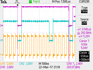
F0005TEK.png [ 76.18 KiB | Viewed 1515 times ]


2. same prog, first write access then jump back and read access
Attachment:
File comment: upper trace RWB - mid trace CS7B - bottom trace PHI2
F0004TEK.png
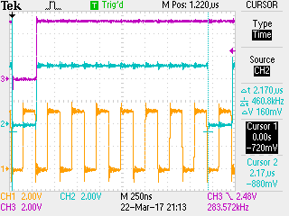
F0004TEK.png [ 76.18 KiB | Viewed 1515 times ]


3. closer look to RWB and CS7B become asserted during PHI2 = 0
Attachment:
File comment: upper trace RWB - mid trace CS7B - bottom trace PHI2
F0006TEK.png
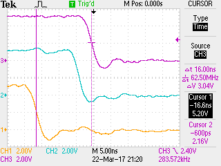
F0006TEK.png [ 76.18 KiB | Viewed 1515 times ]


4. RWB and CS7B were deasserted after PHI2 = 1
Attachment:
File comment: upper trace RWB - mid trace CS7B - bottom trace PHI2
F0007TEK.png
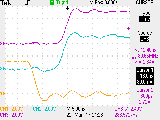
F0007TEK.png [ 76.18 KiB | Viewed 1515 times ]


This looks ways better than what is stated in the datasheet. OK, this way one cannot verify the specs, there are no extreme conditions (temp/voltage/bus load/etc). But at least it gives an idea of whats going on :)


Top
 Profile  
Reply with quote  
PostPosted: Wed Mar 22, 2017 11:02 pm 
Offline
User avatar

Joined: Wed Mar 01, 2017 8:54 pm
Posts: 660
Location: North-Germany
In order to make one post not too lengthy here are 3 more screenshots:

Same conditions, this time software runs in external memory (32KiB on board). The loop reads one byte from long addressed memory, then does a EOR #$FF and writes it back.
Attachment:
File comment: upper trace = D0, medium trace = CS7B, bottom trace = PHI2
F0010TEK.png
F0010TEK.png [ 76.18 KiB | Viewed 1513 times ]

Data ("1") is fetched, inverted, and stored back. But there is no RAM @ DD7722 so next time again a "1" is loaded.

closer look to D0
Attachment:
File comment: upper trace = D0, medium trace = CS7B, bottom trace = PHI2
F0012TEK.png
F0012TEK.png [ 76.18 KiB | Viewed 1513 times ]


Attachment:
File comment: upper trace = D0, medium trace = CS7B, bottom trace = PHI2
F0013TEK.png
F0013TEK.png [ 76.18 KiB | Viewed 1513 times ]


The databus is around 8ns after assertion of PHI2 settled -- so there is plenty time for a RAM to fetch it.

If my 265 isn't an extraordinary superfast exception, running the device with 8MHz or perhaps 10MHz should be possible.


Top
 Profile  
Reply with quote  
PostPosted: Wed Mar 22, 2017 11:46 pm 
Offline

Joined: Sat Dec 13, 2003 3:37 pm
Posts: 1004
Well, from what I can tell.

The W65C816SXB and W65C02SXB boards, i.e. the ones with the discrete MPU and I/O chips, run at 8MHz.

The W65C134SXB and W65C265SXB boards, i.e. the ones with the micro controller with inbuilt peripherals, runs at 3.6864 MHz

The W65C268QBX also runs at 3.6864 MHz.

The discrete MPUs apparently can run up to 14Mhz, but the micro controllers can only run 8MHz.

Curious why their MCU boards don't run at 8MHz.


Top
 Profile  
Reply with quote  
PostPosted: Thu Mar 23, 2017 1:10 am 
Offline
User avatar

Joined: Sun Nov 27, 2011 12:03 pm
Posts: 229
Location: Amsterdam, Netherlands
GaBuZoMeu wrote:
The databus is around 8ns after assertion of PHI2 settled -- so there is plenty time for a RAM to fetch it.

When writing to SRAM, meeting access time is not usually in data setup, but in address setup. I've done a few designs myself with both W65C02 and W65C816, and fast SRAM, and measured the relevant bus timing. In practice address becomes valid roughly 5 ns into the first half cycle and data roughly 5 ns into the second. Imagine address and data as registered at the CPU boundary, clocked on their respective clock edges, and you'd probably be very close to how it's actually implemented.

GaBuZoMeu wrote:
If my 265 isn't an extraordinary superfast exception, running the device with 8MHz or perhaps 10MHz should be possible.

If it's anything like the WDC 65C02 or 65C816, it will run up to around 24 MHz. My designs do. And that's at 3V3.


Top
 Profile  
Reply with quote  
PostPosted: Thu Mar 23, 2017 1:51 am 
Offline
User avatar

Joined: Tue Mar 05, 2013 4:31 am
Posts: 1373
whartung wrote:
Well, from what I can tell.

The W65C816SXB and W65C02SXB boards, i.e. the ones with the discrete MPU and I/O chips, run at 8MHz.

The W65C134SXB and W65C265SXB boards, i.e. the ones with the micro controller with inbuilt peripherals, runs at 3.6864 MHz

The W65C268QBX also runs at 3.6864 MHz.

The discrete MPUs apparently can run up to 14Mhz, but the micro controllers can only run 8MHz.

Curious why their MCU boards don't run at 8MHz.


Page 12 of the datasheet shows the timer values used with various clock speeds to get UART baud rates which are standard. In short, the 3.6864MHz clock allows standard baud rates for the UART which the built-in monitor uses for a console port.

_________________
Regards, KM
https://github.com/floobydust


Top
 Profile  
Reply with quote  
PostPosted: Thu Mar 23, 2017 9:54 pm 
Offline
User avatar

Joined: Wed Mar 01, 2017 8:54 pm
Posts: 660
Location: North-Germany
Well, I open the throttle a bit.

With 11,0592MHz (3x 3,6864MHz) signals are quite acceptable:
Attachment:
File comment: Top: D0; Center: CS7B; Bottom: PHI2
F0008TEK.png
F0008TEK.png [ 76.18 KiB | Viewed 1450 times ]


Next to 4x 3,6864 I used 15,0 MHz:
Attachment:
File comment: Top: D0; Center: CS7B; Bottom: PHI2
F0010TEK.png
F0010TEK.png [ 76.18 KiB | Viewed 1450 times ]


Now the 16..17ns delay PHI2fall to CS7=0 as well as nearly 20ns from PHI2rise to D0=1 becomes pretty prominent.

Next try with 22,1184MHz didn't work - but may be the quartz was unsuitable. It simply won't oscillate.

So far I'm quite confident with these results. Using 11,0592MHz seems to me an acceptable choice.


Top
 Profile  
Reply with quote  
PostPosted: Thu Mar 23, 2017 11:57 pm 
Offline

Joined: Sat Dec 13, 2003 3:37 pm
Posts: 1004
GaBuZoMeu wrote:
So far I'm quite confident with these results. Using 11,0592MHz seems to me an acceptable choice.


On startup the monitor in the embedded ROM tries to determine the clock rate of the CPU, and it looks like it uses that setting to set up the baud rates. It seems to recognize the following clock rates:

;0 = 1.843200MHZ
;1 = 2.457600MHZ
;2 = 3.686400MHZ
;3 = 4.915200MHZ
;4 = 6.144000MHZ

So if you crank up the speed, you'll need to set up the UARTs yourself.

Also, on start up if you have the letters WDC at $00:8000, the monitor, on reset, will JMP to $00:8003. Same with $00:0800-00:0803, it checks that if the first check fails. So if you were to wire up a custom ROM, you'll need something at $00:8000 or $00:0800 to pre-empt the monitor and get control of the CPU, ports, and chip selects.

This board is wired to use the internal ROM, it doesn't look straightforward to be able to disable the internal ROM at start up, since that takes some timing chicanery and the pins you need access to aren't readily available (they're not on either of the headers).


Top
 Profile  
Reply with quote  
PostPosted: Sat Mar 25, 2017 10:20 am 
Offline
User avatar

Joined: Wed Mar 01, 2017 8:54 pm
Posts: 660
Location: North-Germany
I have tried 4,9152MHz and 6,144MHz by removing the original quarz and replace them with others. They start oscillating but somehow the monitor fails to setup the divider values for the uart :( - you get only the usual garbage having false baudrates settings.

I haven't try to figure out what sort of baudrates the monitor establishes (by scoping). Selecting 4800 and 19200 at the terminal side gave no success.


Top
 Profile  
Reply with quote  
PostPosted: Sat Mar 25, 2017 12:37 pm 
Offline
User avatar

Joined: Tue Mar 02, 2004 8:55 am
Posts: 996
Location: Berkshire, UK
From memory I think it defaults to 9600 baud

_________________
Andrew Jacobs
6502 & PIC Stuff - http://www.obelisk.me.uk/
Cross-Platform 6502/65C02/65816 Macro Assembler - http://www.obelisk.me.uk/dev65/
Open Source Projects - https://github.com/andrew-jacobs


Top
 Profile  
Reply with quote  
PostPosted: Sat Mar 25, 2017 6:33 pm 
Offline
User avatar

Joined: Wed Mar 01, 2017 8:54 pm
Posts: 660
Location: North-Germany
BitWise wrote:
From memory I think it defaults to 9600 baud

Correctly, there is a default case in the monitor rom. But the previous attempt to figure out how fast FCLK may be is buggy. Obviously this was never ever verified ...


Top
 Profile  
Reply with quote  
PostPosted: Sat Mar 25, 2017 9:35 pm 
Offline

Joined: Sat Dec 13, 2003 3:37 pm
Posts: 1004
The code for the check is in the monitor listing, it may be worthwhile to dis-assemble that part of the monitor and see if it matches the listing. I don't recall the exact details, but, simply it starts some kind of timer, sets X to $1000, and then DEXes it to zero. At that point it checks the timer value. There's 2 lookup tables, one for a low range, and the other for a high range. It then compares the timer value against those ranges, trying to find which set matches. The end result is X is set with 0-4, and then that is used to look up in another table the defaults to set up the UART.

So, it may be worthwhile to try and hunt down what the monitor is doing, dis-assemble and duplicate it, and see if/how badly off the lookup tables are.


Top
 Profile  
Reply with quote  
PostPosted: Sun Mar 26, 2017 12:42 am 
Offline
User avatar

Joined: Wed Mar 01, 2017 8:54 pm
Posts: 660
Location: North-Germany
You are fully right. I only look at the listing didn't disaasemble the code. But as I tried the "legal" quarz frequencies (above 3,6864MHz) and it wasn't successful, there is a good chance that the listing is up to date.

Looking at the listing there is one bad mistake: the loop (4096x5cycles) is too long. It lasts more than 256 cycles of 32KHz. But they use only the lower byte of T2 for comparison. The lengthy loop causes the possible results to be neither ascending nor descending. Finally the compare is too simple, it would only work with descending values or if they would branch back to the first table if the second compare fails.

But this is not too much a problem. In the very moment one is going to add some more software, one can correct this. ;)


Top
 Profile  
Reply with quote  
PostPosted: Sun Mar 26, 2017 4:26 am 
Offline

Joined: Sat Dec 13, 2003 3:37 pm
Posts: 1004
GaBuZoMeu wrote:
Looking at the listing there is one bad mistake: the loop (4096x5cycles) is too long. It lasts more than 256 cycles of 32KHz. But they use only the lower byte of T2 for comparison.


I don't think that's really a problem, but I know it looks funny as the values have no relationship to each other.

But even though they're only looking at the bottom byte, they actually have a higher resolution solution. They probably found that the upper was too low of a resolution to find what they were looking for.

I mean, you'd no best since you can duplicate the test (by swapping the xtals) and see what they get.

But, in the end, yea, the value ranges they test for in fact have no actual relation to each other. No doubt they were arrived at experimentally.


Top
 Profile  
Reply with quote  
Display posts from previous:  Sort by  
Post new topic Reply to topic  [ 49 posts ]  Go to page Previous  1, 2, 3, 4  Next

All times are UTC


Who is online

Users browsing this forum: No registered users and 7 guests


You cannot post new topics in this forum
You cannot reply to topics in this forum
You cannot edit your posts in this forum
You cannot delete your posts in this forum
You cannot post attachments in this forum

Search for:
Jump to: