6502.org Forum  Projects  Code  Documents  Tools  Forum
It is currently Sun Apr 28, 2024 4:17 am

All times are UTC


Post new topic Reply to topic  [ 57 posts ]  Go to page 1, 2, 3, 4  Next
Author Message
PostPosted: Sat Sep 17, 2016 2:21 pm 
Offline
User avatar

Joined: Mon May 25, 2015 2:25 pm
Posts: 632
Location: Gillies, Ontario, Canada
Fusion-6502 is a project inspired from my giant breadboard project called "Vulcan-74".
The original goal was to simply emulate the hardware on an FPGA so I could make the hardware more portable.
Being on the road a lot, I wanted to have a way to code 6502 assembly that could travel with me.

After some progress, I decided that this project has become something much more, which is why I started a new thread.
All further progress and discussion on Fusion-6502 will be posted to this thread.
Here is the intro from the other thread, describing the hardware....

The target is a Spartn-6 FPGA, and the "donor" board was once a Mojo-FPGA Board. I say donor because I hacked it all to hell. The Mojo board is a great FPGA board, by the way!

I needed a meg of SRAM, so I dead-bugged a pair of 512K SRAMs to the board, and then replaced the oscillator with a 20MHz clock.
The FPGA is clocked at 40MHz, and does some real trickery when it comes to sharing the SRAM with 6502, Video, Sound, and GPU.

The 6502 thinks it is just connected to a super fast 64K SRAM, and the FPGA does all the boot load stuffing and IO magic.
I am also working on some SD Card code to load everything on startup, but for now it is all done via SB cable.

The FPGA version actually has more power than the breadboard version, since it is easy to add features in code.
Some of the extra features include...

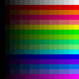
- 4096 color programmable palette that can display 256 colors at once.
- Single cycle 32 bit math accessible by the 6502.
- Graphics functions such as line, box, circle, fill, and text (C64 Font) built in.
- Sprite rotations for every 90 degrees, including mirror image.
- Horizontal and Vertical image sheering for ultra fast Wolfenstien-like ray trace games.
- Built in math stuff like Sin, Cos, Collision Detection, etc.
- Polygon fill routine.

I also plan to emulate my unfinished Sound Engine, which will be like an 8 channel Amiga.

This quick hack turned out so well that I decided to give it an official title... "Fusion-6502".
It's basically a chipset for a real 6502! Sound graphics and IO from a single FPGA.

Ok, here is the obligatory eye candy....

Image
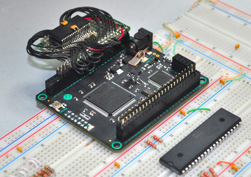
This was once a MOJO Fpga board.

To gain the required 98 IO pins, I desoldered all of the onboard LEDs and made a new IO map.
I also ripped up the oscillator and added a new 20MHz version.
This is doubled internally by the PLL to meet the 40MHz timing for 800x600 VGA.

Image
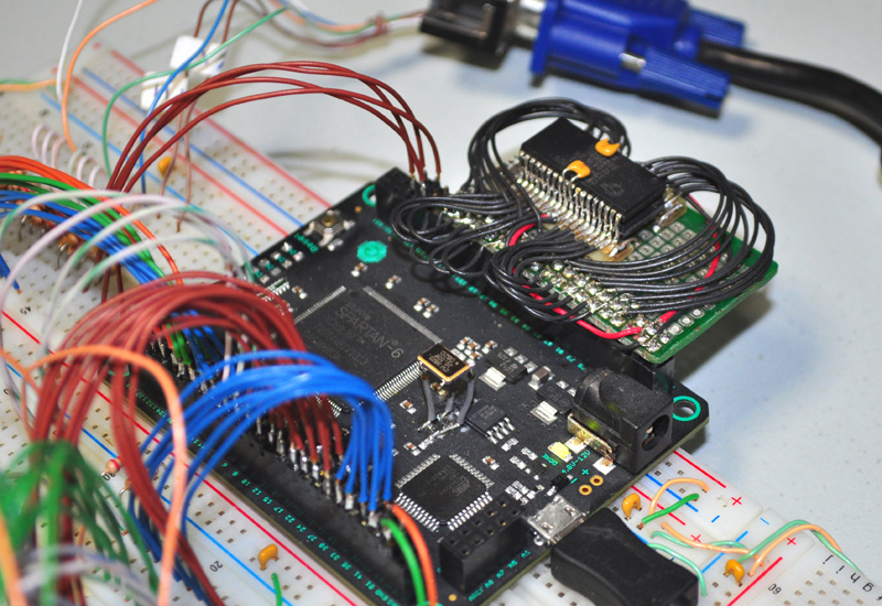
A pair of 512K 10ns SRAMs added.

Everything is shared by the 1 meg of onboard memory, arbitrated by the FPGA.
Zero page and IO live internally in code, but everything else is in SRAM.
Graphics Data, Sound Data, 6502 Code, and dual Video Buffers all take tuns!
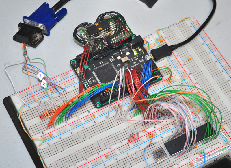
Image
6502 and Video DAC

The 6502 has no idea that it is connected to an FPGA!
I have tested the 6502 up to 8MHz, which is the "legal" top speed for 3.3v operation.
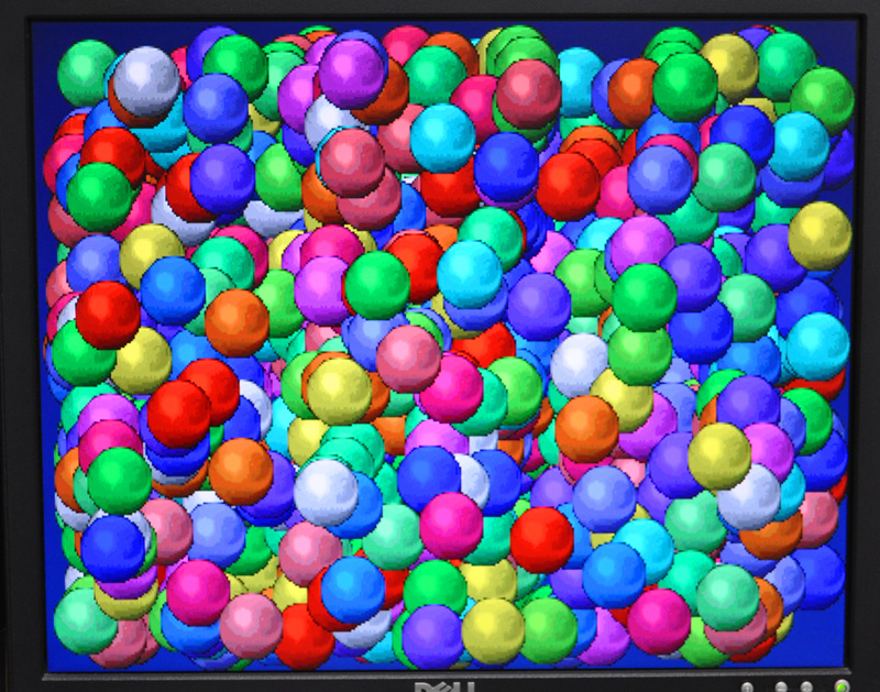
As you can see by the resulting videos, this is plenty fast to womp an Amiga for graphics power!

The Video DAC is 12 bits, for a total of 4096 colors. Only 256 are displayed at once.
To allow for more color control, the palette is fully programmable on the fly.

Image
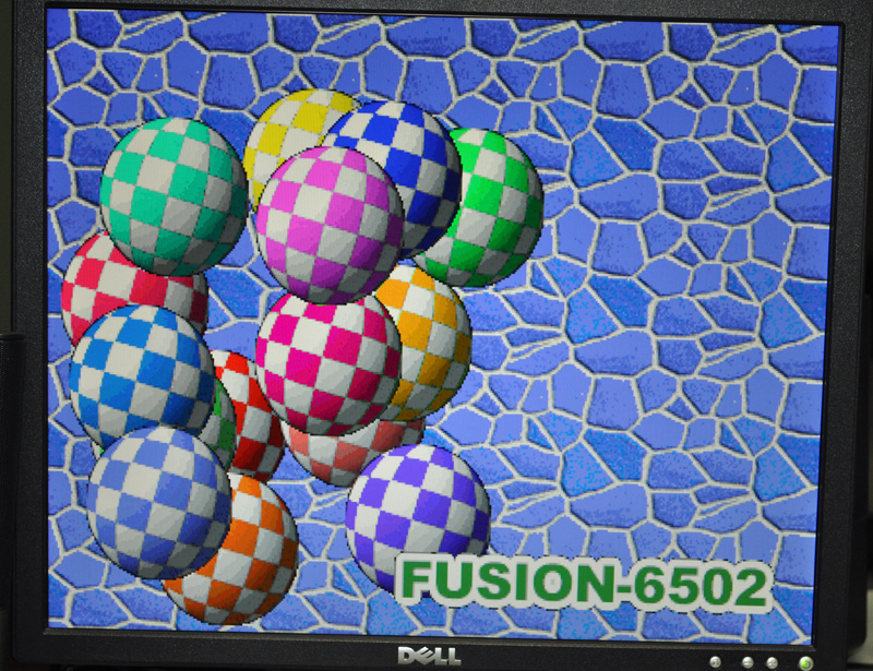
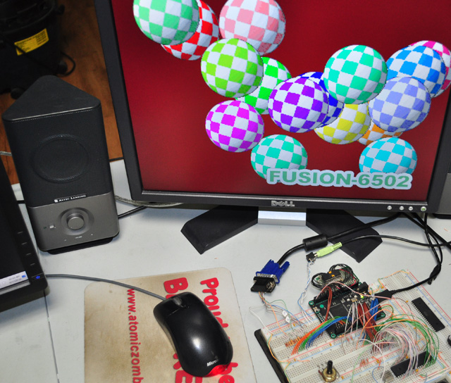
It's those damn checker balls again!!

Yeah, what can I say... I like watching those checker balls fly around the screen!
This time they are multi-colored thanks to the abilty to rotate the color palette on the fly.
I only have to store one 32 color ball sequence, and can rotate the dark panels 16 times.

These ar 80x80 sprites with 256 color depth, and one invisible "alpha" color.
Fusion-6502 can hurl over 30 of these around the screen at 60 frames per second!
For comparison "Boing" on the Amiga only did one ball, and it was only color cycled.

I started this project at 8:00am this morning, but did not complete the Sound System yet.
Not too bad for a day's work, and I will complete the Sound System on the next free rainy day!

Here is a video of it working...

https://youtu.be/CNVghL233FI

Anyone interested in a board for this project? It's a great platform to test 6502 assembly on!
I would probably provide it with everything minus the 65C02, which would drop into a DIP socket.

OK, back to my farm until the next rain or snow day.
Thanks again for this website!

Cheers,
Radical Brad


Last edited by Oneironaut on Thu Mar 16, 2017 5:17 pm, edited 1 time in total.

Top
 Profile  
Reply with quote  
PostPosted: Sat Sep 17, 2016 2:50 pm 
Offline
User avatar

Joined: Mon May 25, 2015 2:25 pm
Posts: 632
Location: Gillies, Ontario, Canada
I have continued to develop Fusion-6502 in a very odd way... using only Notepad!
Every time I have a small break from my job in the city, I just write Verilog code in Notpad.
I then dump the code into Xilinx ISE when I get home and compile it.
Most of the time, the new routines work, as Verilog is actually very easy to use once you know your hardware.

Yesterday, I added functions for 32 bit Addition, Subtraction, Multiplication, and Division.
The 6502 can call these functions in only a few cycles!

All math is done by writing two 16 bit values to the memory mapped IO space in the FPGA.
The result is then read as bytes from the FPGA. The 6502 always thinks it's simply talking to SRAM.

I decided to make all math functions accept a 16 bit value, and the return value will be 32 bits.
So for most math functions, the 6502 might only need to send 2 8 bit values and read one or two bytes back.
It can however send two 16 bit values and read back a full 32 bit value for something like 16x16=32 bit division or multiplication.
The FPGA does it all in a single cycle at 40MHz!

The code required in Verilog was sinfully simple!
I won't pollute this thread with too much Verilog, as my focus is the 6502, but check this snippet out...

Code:
///////////////////////////////////////////////////////////////////////////////////////////////////////////////////////////////////////////////////////////////////
////////// COMMAND 700 : SET MATH INPUT VALUE A.LO
////////// DATA : ADRESS VALUE HI
///////////////////////////////////////////////////////////////////////////////////////////////////////////////////////////////////////////////////////////////////
if (COMMAND == 700 & COMSTEP == 1) begin
MATHA[7:0] <= COMDATA;
COMSTEP <= 255;
end

///////////////////////////////////////////////////////////////////////////////////////////////////////////////////////////////////////////////////////////////////
////////// COMMAND 701 : SET MATH INPUT VALUE A.HI
////////// DATA : ADRESS VALUE HI
///////////////////////////////////////////////////////////////////////////////////////////////////////////////////////////////////////////////////////////////////
if (COMMAND == 701 & COMSTEP == 1) begin
MATHA[15:8] <= COMDATA;
COMSTEP <= 255;
end

///////////////////////////////////////////////////////////////////////////////////////////////////////////////////////////////////////////////////////////////////
////////// COMMAND 702 : SET MATH INPUT VALUE B.LO
////////// DATA : ADRESS VALUE HI
///////////////////////////////////////////////////////////////////////////////////////////////////////////////////////////////////////////////////////////////////
if (COMMAND == 702 & COMSTEP == 1) begin
MATHB[7:0] <= COMDATA;
COMSTEP <= 255;
end

///////////////////////////////////////////////////////////////////////////////////////////////////////////////////////////////////////////////////////////////////
////////// COMMAND 703 : SET MATH INPUT VALUE B.HI
////////// DATA : ADRESS VALUE HI
///////////////////////////////////////////////////////////////////////////////////////////////////////////////////////////////////////////////////////////////////
if (COMMAND == 703 & COMSTEP == 1) begin
MATHB[15:8] <= COMDATA;
COMSTEP <= 255;
end

///////////////////////////////////////////////////////////////////////////////////////////////////////////////////////////////////////////////////////////////////
////////// COMMAND 704 : MATH FUNCTION : C = A + B
////////// DATA : NOT USED
///////////////////////////////////////////////////////////////////////////////////////////////////////////////////////////////////////////////////////////////////
if (COMMAND == 704 & COMSTEP == 1) begin
MATHR <= MATHA + MATHB;
COMSTEP <= 255;
end

///////////////////////////////////////////////////////////////////////////////////////////////////////////////////////////////////////////////////////////////////
////////// COMMAND 705 : MATH FUNCTION : C = A - B
////////// DATA : NOT USED
///////////////////////////////////////////////////////////////////////////////////////////////////////////////////////////////////////////////////////////////////
if (COMMAND == 705 & COMSTEP == 1) begin
MATHR <= MATHA - MATHB;
COMSTEP <= 255;
end

///////////////////////////////////////////////////////////////////////////////////////////////////////////////////////////////////////////////////////////////////
////////// COMMAND 706 : MATH FUNCTION : C = A * B
////////// DATA : NOT USED
///////////////////////////////////////////////////////////////////////////////////////////////////////////////////////////////////////////////////////////////////
if (COMMAND == 706 & COMSTEP == 1) begin
MATHR <= MATHA * MATHB;
COMSTEP <= 255;
end

///////////////////////////////////////////////////////////////////////////////////////////////////////////////////////////////////////////////////////////////////
////////// COMMAND 707 : MATH FUNCTION : C = A / B
////////// DATA : NOT USED
///////////////////////////////////////////////////////////////////////////////////////////////////////////////////////////////////////////////////////////////////
if (COMMAND == 707 & COMSTEP == 1) begin
MATHR <= MATHA / MATHB;
COMSTEP <= 255;
end

///////////////////////////////////////////////////////////////////////////////////////////////////////////////////////////////////////////////////////////////////
////////// COMMAND 708 : READ MATH RESULT BIT 0 OF 3
////////// DATA : NOT USED
///////////////////////////////////////////////////////////////////////////////////////////////////////////////////////////////////////////////////////////////////
if (COMMAND == 708 & COMSTEP == 1) begin
CPUSEND <= MATHR[7:0];
COMSTEP <= 255;
end
///////////////////////////////////////////////////////////////////////////////////////////////////////////////////////////////////////////////////////////////////
////////// COMMAND 709 : READ MATH RESULT BIT 1 OF 3
////////// DATA : NOT USED
///////////////////////////////////////////////////////////////////////////////////////////////////////////////////////////////////////////////////////////////////
if (COMMAND == 709 & COMSTEP == 1) begin
CPUSEND <= MATHR[15:8];
COMSTEP <= 255;
end
///////////////////////////////////////////////////////////////////////////////////////////////////////////////////////////////////////////////////////////////////
////////// COMMAND 710 : READ MATH RESULT BIT 2 OF 3
////////// DATA : NOT USED
///////////////////////////////////////////////////////////////////////////////////////////////////////////////////////////////////////////////////////////////////
if (COMMAND == 710 & COMSTEP == 1) begin
CPUSEND <= MATHR[23:16];
COMSTEP <= 255;
end
///////////////////////////////////////////////////////////////////////////////////////////////////////////////////////////////////////////////////////////////////
////////// COMMAND 711 : READ MATH RESULT BIT 3 OF 3
////////// DATA : NOT USED
///////////////////////////////////////////////////////////////////////////////////////////////////////////////////////////////////////////////////////////////////
if (COMMAND == 711 & COMSTEP == 1) begin
CPUSEND <= MATHR[31:24];
COMSTEP <= 255;
end


The code above shows how each command (read or write) is assigned to the IO space of 512 to 767, just above the hardware stack.
The FPGA intercepts this address, and does what it has to do before at 40MHz, so that the 6502 is not waiting for anything.

The named registers above are part of the IO subsystem, that allow the 6502 to belive that it is talking to 10ns SRAM...

COMMAND : This is the intercepted 16 Bit address from the 6502.
DATA : This is the intercepted 8 Bit Data value from the 6502.
COMSTEP : This is a pipeline for internal FPGA functions. Some need more than 1 cycle like Sprite Commands.
COMSEND : This is the value sent to the bidirectional Data port, which is controlled by the 6502 RW line.
MATHA/B: These are just 16 bit registers in the FPGA used as math input values.
MATHR : This is a 32 bit FPGA register to hold the reulting math value.

So the 6502 would simply do the following in order to calculate the result of something like : 62100 / 889...

- Write the value of LO8(62100) to address 700
- Write the value of HI8(62100) to address 701
- Write the value of LO8(889) to address 702
- Write the value of HI8(889) to address 703

- Write to address 707 to trigger the Division Command

- Read the value (Result Byte 0/1) at address 708
- Read the value (Result Byte 1/1) at address 709
- Read the value (Result Byte 2/1) at address 710
- Read the value (Result Byte 3/1) at address 711

Now this may seem like quite a few steps, but imagine the number of cycles that would be required for 6502 only assembly to do this!
.... hundreds, possibly thousands of machine cycles?


Anyhow, since this project has taken on a life of its own now, I am now considering a few other options.
Adding a Vinculum chip to allow a USB keyboard for input and a USB stick for storage would be nice.
Originally, I planned for only joystick and a 1mb SPI flash to boot, but the USB stick would make cross-dev easy.

The original goal of using a REAL 6502 will not change no matter how advanced the support hardware becomes.
The goal is to enjoy 6502 coding on a real 6502, and the rest is just an enhanced multimedia chip-set.
The 6502 will still only see 64K of program space, and will be running at speeds between 8 MHz and 14 MHz.

Even the final board layout will put the 6502 right in the center of the board, and possibly the rest on the underside.
It is my intent to give the 6502 the home it deserves! The FPGA is just a minion to do its multimedia bidding!

Ok, now that I have started yet another project, I will update when I have time!

Image

Cheers!
Radical Brad


Top
 Profile  
Reply with quote  
PostPosted: Sun Sep 18, 2016 11:15 pm 
Offline
User avatar

Joined: Mon May 25, 2015 2:25 pm
Posts: 632
Location: Gillies, Ontario, Canada
Back in the 80's, after staring at a wavering 12 inch NTSC monitor for 5 hours, I finally made 8 sprites move across the screen on my C64.
They were only 12x21 in size with 4 colors, but it was cool to finally see them come to life.

32 years later, I have made another 6502 powered Sprite Test program.
This time, I managed to move 1000 Sprites of 32x32 size and 256 colors!...

Image
1000 Sprites equates to 1,024,000 8 bit pixels!

Actually, the full number is over 1000, but I can't remember by how much.
I just stopped adding 10 at a time right before the frame rate dropped under 60 FPS.

Here is a video...
https://youtu.be/GrsY4SpFpHs

This test is actually demonstrating the Sprite Palette Color Remapping function inside the FPGA.
What I did was store only a single 32x32 ball sprite using 16 shades of color.
The 6502 then commands the GPU to shift the pallette by 16 steps for each sprite draw.
Since my internal Palette is 16 shades of 16 colors, this works very well...

Image
This is the Default Fusion-6502 Palette

Fusion-6502 has a 12 Bit DAC, so it can display 4096 different colors.
Internally, it only uses 8 bit color, so 256 colors can be displayed at once.
The palette is fully definable as well.

Here is the only Sprite stored in memory...

Image

Fusion GPU has a selectable "Alpha" color, so in the Sprite above, that is color zero (Black).
Since each row of color shades starts with black, this also keeps the Alpha color correct.


I am now fine tuning the way the FPGA talks to the 6502 to get optimal IO bandwidth.
There is a learning curve for me here, as I don't fully know what happens inside the 6502 for each instruction.
The FPGA controls the 6502 clock, and listens for certain addresses, and it must also give back as expected.

Time to dig into the datasheets and books!

Later!
Radical Brad


Top
 Profile  
Reply with quote  
PostPosted: Mon Sep 19, 2016 5:09 pm 
Offline
User avatar

Joined: Mon May 25, 2015 2:25 pm
Posts: 632
Location: Gillies, Ontario, Canada
Had a response from FTDIChip on their amazing Vinculum chip, which is a single chip dual USB host controller solution.
I asked them if the VII would allow simultaneous USB keyboard host and USB stick support, and the short answer was yes.

http://www.ftdichip.com/Products/ICs/VNC2.htm

Now that Fusion-6502 has proven to be a worthy project, I am looking at options to give it real world connectivity.
The goal is to make a fun platform for 6502 assembly, with a focus on games and demos, so I need input (storage & human).
Rather than just a 4 position joystick, I thought that a keyboard would be better.
I will not use a PS2 keyboard, so besides hacking the internal matrix, USB is the only other option.

I also need to get program code and multimedia files into the SRAM (1 Meg so far) on the board.
Originally, I though of just using a single 1mb SPI flash, but that has limitations.
Since I will be coding 6502 assembly on my PC, it would be nice to have a cross compatible storage medium.
A USB stick would be nice, as I could add FAT16/32 support right into the FPGA and let the 6502 open files.

Does any one here have any experience with the Vinculum?
Seems that they offer their own IDE and decent examples.
It looks so easy that I want to speak with someone who has used the chip.

My goal is to add a USB OTG keyboard host and USB drive support.
I do not want to become a USB guru, I just want the basics.
Seems like that's what Vinculum is all about.

If this becomes too complex, then I will probably just do a tutorial on how to hack any keyboard to jack into the matrix.
Any low end PIC or AVR can be used to read a PC keyboard matrix, and spit out bytes.
As for storage, without USB, I would have to fall back to SDCards, which is an ugly solution thee days with SPI being phased out.

My free time will still be going into making the 6502 <-> FPGA port most efficient, and then I will worry about the controller and storage.

Brad


Top
 Profile  
Reply with quote  
PostPosted: Tue Sep 20, 2016 12:53 pm 
Offline
User avatar

Joined: Mon May 25, 2015 2:25 pm
Posts: 632
Location: Gillies, Ontario, Canada
Working on Fusion-6502 during work breaks! Small steps are being made.

In order to aid development, I created a program in Visual Studio that takes the binary output from 6502 Macroassembler and spits out a Verilog ROM file. On powerup, the FPGA then dumps these values into the 64K segment of the external SRAM that the 6502 considers its own.

I also added that 32x32 Ball Sprite into the FPGA as a ROM, and it is dumped to the start of Multimedia Memory on power up.

This will make fine tuning much easier as I test the real 6502, to its limits running at 3.3 volts.
I realized that I was overthinking what happens inside the 6502 for each true clock cycle, and that it really doesn't matter since the FPGA simply holds PHI2 high when it needs to. The 6502 really only does two things; reading and writing to an address. Since the FPGA simulates SRAM to the 6502 and captures any data coming and going between address 512 and 767, the 6502 can simply function normally.

So far, here are all of the working functions inside the Fusion-6502 GPU...


Code:
////////// COMMAND 512 : FLIP VIDEO PAGES ON VSYNC
////////// COMMAND 513 : CLEAR THE ENTIRE VIDEO SCREEN
////////// COMMAND 514 : DRAW PIXEL TO BACK PAGE USING DRAWX1 AND DRAWY1
////////// COMMAND 515 : SET DRAW LOCATION X1.LO
////////// COMMAND 516 : SET DRAW LOCATION X1.HI
////////// COMMAND 517 : SET DRAW LOCATION Y1.LO
////////// COMMAND 518 : SET DRAW LOCATION Y1.HI
////////// COMMAND 519 : SET DRAW LOCATION X2.LO
////////// COMMAND 520 : SET DRAW LOCATION X2.HI
////////// COMMAND 521 : SET DRAW LOCATION Y2.LO
////////// COMMAND 522 : SET DRAW LOCATION Y2.HI
////////// COMMAND 523 : SET SPRITE GRAPHICS ADDRESS LO
////////// COMMAND 524 : SET SPRITE GRAPHICS ADDRESS MD
////////// COMMAND 525 : SET SPRITE GRAPHICS ADDRESS HI
////////// COMMAND 526 : SET SPRITE ALPHA COLOR
////////// COMMAND 527 : DRAW SPRITE FROM SPRITE ADDRESS TO DRAWX1,DRAWY1,DRAWX2,DRAWY2
////////// COMMAND 528 : SET DRAW GRAPHICS ADDRESS LO
////////// COMMAND 529 : SET DRAW GRAPHICS ADDRESS MD
////////// COMMAND 530 : SET DRAW GRAPHICS ADDRESS HI
////////// COMMAND 531 : DRAW PIXEL TO GFXMEM USING DRAW ADDRESS & POST INC
////////// COMMAND 532 : SET SPRITE ALPHA MODE
////////// COMMAND 533 : SET ALTERNATE PALETTE INDEX
////////// COMMAND 534 : SET ALTERNATE PALETTE AT INDEX AND POST INC
////////// COMMAND 535 : DRAW BITMAP FROM GFXADR TO DRAWX1,DRAWY1,DRAWX2,DRAWY2
////////// COMMAND 536 : SET TEXT TEXT COLOR
////////// COMMAND 537 : DRAW TEXT USING DRAWX1,DRAWY1,TEXTCOLOR
////////// COMMAND 538 : SET VGA PALETTE INDEX
////////// COMMAND 539 : SET VGA PALETTE LO
////////// COMMAND 540 : SET VGA PALETTE HI AT INDEX AND POST INC
////////// COMMAND 541 : READ PIXEL FROM GFXMEM USING DRAW ADDRESS & POST INC
////////// COMMAND 600 : SET SOUND FREQUENCY LO
////////// COMMAND 601 : SET SOUND FREQUENCY HI
////////// COMMAND 602 : SET SOUND VOLUME
////////// COMMAND 603 : SET SOUND START ADDRESS LO
////////// COMMAND 604 : SET SOUND START ADDRESS MD
////////// COMMAND 605 : SET SOUND START ADDRESS HI
////////// COMMAND 606 : SET SOUND END ADDRESS LO
////////// COMMAND 607 : SET SOUND END ADDRESS MD
////////// COMMAND 608 : SET SOUND END ADDRESS HI
////////// COMMAND 609 : SET SOUND LOOPS AND PLAY
////////// COMMAND 610 : SET SOUND VOICE NUMBER
////////// COMMAND 700 : SET MATH INPUT VALUE A.LO
////////// COMMAND 701 : SET MATH INPUT VALUE A.HI
////////// COMMAND 702 : SET MATH INPUT VALUE B.LO
////////// COMMAND 703 : SET MATH INPUT VALUE B.HI
////////// COMMAND 704 : MATH FUNCTION : C = A + B
////////// COMMAND 705 : MATH FUNCTION : C = A - B
////////// COMMAND 706 : MATH FUNCTION : C = A * B
////////// COMMAND 707 : MATH FUNCTION : C = A / B
////////// COMMAND 708 : READ MATH RESULT BIT 0 OF 3
////////// COMMAND 709 : READ MATH RESULT BIT 1 OF 3
////////// COMMAND 710 : READ MATH RESULT BIT 2 OF 3
////////// COMMAND 711 : READ MATH RESULT BIT 3 OF 3
////////// COMMAND 712 : MATH FUNCTION : SIN


Commands are in no particular order at this time, and I plan to sort them logically later.

The 1024K of memory strapped to the FPGA is used as follows...

Code:
// ADDRESS : 0000000 TO 0065535 = 064K : 6502 DEDICATED MEMORY
// ADDRESS : 0065536 TO 0185535 = 120K : SCREEN MEMORY PAGE ONE
// ADDRESS : 0185536 TO 0305535 = 120K : SCREEN MEMORY PAGE TWO
// ADDRESS : 0305536 TO 1048575 = 743K : GRAPHICS AND SOUND


The 64K segment dedicated to the 6502 is mapped as follows...

Code:
// ADDRESS : 00000 TO 00255 = 00256B : ZERO PAGE RAM
// ADDRESS : 00256 TO 00511 = 00256B : HARDWARE STACK
// ADDRESS : 00512 TO 00767 = 00256B : CONTROL PORT
// ADDRESS : 00768 TO 65529 = 64762B : PROGRAM MEMORY
// ADDRESS : 65530 TO 65531 = 00002B : NMI VECTOR
// ADDRESS : 65532 TO 65533 = 00002B : RESET VECTOR
// ADDRESS : 65534 TO 65535 = 00002B : BRK VECTOR

// RESET VECTOR SET TO PROGRAM MEMORY @ ADDRESS 00768
// RESET VECTOR VALUES : 65532 = 000 / 65533 = 003


Screen Memory is a set of 120K segments that are mapped directly to the 400x300 video frame.
The GPU is always dispaying one page, while drawing to the other. This is a "Double Buffer"
The 6502 issues the Flip Command (512) to exchange these buffers.
Screen Memory is seen as a rectangular 400 x 300 Bytes.

Graphics and Sound Memory is a serial stream of memory, which is why its address is 24 bits.
Sprites, Samples, and Bitmaps are "streamed" from this memory to some destination X / Y location on the Draw Page.
Using a stream makes more since as it eliminates paging and will allow samples and images to be stored efficiently.

The Command Number is simply the address that the FPGA intercepts.
So when the 6502 writes the value of 15 to address 513, the following happens...

1) The FPGA understands that address 513 is the Command for Clear The Drawing Buffer.
2) The 6502 is frozen in time by the FPGA by holding its clock in the high state.
3) The FPGA now writes the value of 15 (Color White) to the 120,000 bytes that make up the Draw Buffer.
4) When the Command has completed, the FPGA continues to offer the clock back to the 6502.

A Command that issues data back to the 6502 works in a similar manner, and the RW line tells the FPGA the data direction.


Once I have several 6502 assembler programs tested, I will get working on some kind of external memory.
I still like the USB Stick idea, as I can just dump the .65b file from the assembler on the stick and then into the Fusion-6502 port.

I am also considering a "Direct Bridge Mode" where Fusion-6502 acts like a USB stick to the PC, so that I can cross develop 6502 code without having to swap anything back and forth.

Fusion-6502 will also "Stuff" a small Boot Menu GUI into the 6502 program memory on power up so that the user can navigate multiple files on the USB stick and load them. There will be no Load "*",8,1 type of thing happening, but the retro feel will certainly be there!

Currently, the FPGA is clocked at 40MHz, so it issues the 6502 clock divided by 5 for 8 MHz. This keeps to the datasheet spec for 3.3v, but I will certainly be pushing to find the real limits once I know everything is stable. If I feel the need for real speed, I may install level translators and pump the 6502 voltage up to 5 volts.

So much fun.
The 6502 never had such a good home!
After this, I will be trying my HDMI engine in the same FPGA.
I have now filled 47% of the Spartan-6 (XC6SLX9), so there is lots of room to grow.

Cheers,
Radical Brad


Top
 Profile  
Reply with quote  
PostPosted: Tue Sep 20, 2016 5:28 pm 
Offline

Joined: Wed Mar 02, 2016 12:00 pm
Posts: 343
Very neat! :mrgreen:

Do the GPU/6502 access memory in turns or within the same cycle?


Top
 Profile  
Reply with quote  
PostPosted: Tue Sep 20, 2016 6:14 pm 
Offline
User avatar

Joined: Mon May 25, 2015 2:25 pm
Posts: 632
Location: Gillies, Ontario, Canada
Thanks!

The memory sharing is the real magic show in this project.
Here is how I pulled the rabbit out of the hat to get away with a single SRAM...

The state machine is divided into 1056 clocks at 40 MHz to match the 800x600 VGA spec.
During this 1056 clocks, which is one complete horizontal timing period, the following happens...

1) From 0 to 399, the SRAM is read, and pixel data from the Live Buffer is stored to FPGA dual port Block Ram.
2) From 400 to 407, SRAM is read to retrieve 8 audio samples (1 per Voice) based on the frequency counter.
3) At steps 1 and 2, the 6502 and GPU logic is restricted from accessing the SRAM.
4) After clock 407, the 6502 gets a divided (and controlled) clock at 5Mhz.
5) If the GPU detects any access to SRAM 512-767, the GPU will hold back the 6502 and execute that command.
6) The GPU must also be aware of steps 1 and 2 during execution, as most commands read or write SRAM.
7) When the GPU has completed a command, it continues to send the 6502 clock.

Also, after the initial 88 clocks, the VGA logic is sending the data from Block Ram to the screen.
Since the Line buffer is always ahead of the count, this works well.
Also note that Every line is sent twice, as the resolution is 400x300 out of 800x600.
This opens up 1056 - the 8 audio reads for full access by the GPU or 6502.

As you can see by my post showing 1000 sprites moving at 60 FPS, the system is blazingly fast!

For the curios, here is myVerilog code segment that buffers in a line of pixels ahead of the Horizontal draw...


Code:
///////////////////////////////////////////////////////////////////////////////////////////////////////////////////////////////////////////////////////////////////
////////// GET 400 PIXELS FROM SRAM AND STORE TO LINE MEMORY
///////////////////////////////////////////////////////////////////////////////////////////////////////////////////////////////////////////////////////////////////

// RESET LINE MEMORY ADDRESS
if (VCOUNT[0] == 0 & VCOUNT < 600 & HCOUNT == 18) SRAMADR <= ((VCOUNT >> 1) * 400) + LIVEPAGE;

// STORE PIXELS TO LINE MEMORY
if (VCOUNT[0] == 0 & VCOUNT < 600 & HCOUNT > 18 & HCOUNT < 418) begin
LINEMEM[HCOUNT-19] <= SRAMDAT;
SRAMADR <= SRAMADR + 1;
end


///////////////////////////////////////////////////////////////////////////////////////////////////////////////////////////////////////////////////////////////////
////////// SEND 400 PIXELS FROM LINE MEMORY
///////////////////////////////////////////////////////////////////////////////////////////////////////////////////////////////////////////////////////////////////

// SEND COLORS FROM PALETTE
if (VCOUNT < 600 & HCOUNT > 87 & HCOUNT < 888) begin
VGARED <= VGAPAL[LINEMEM[(HCOUNT-88)>>1]][3:0];
VGAGRN <= VGAPAL[LINEMEM[(HCOUNT-88)>>1]][7:4];
VGABLU <= VGAPAL[LINEMEM[(HCOUNT-88)>>1]][11:8];

// END OF HORIZONTAL LINE
end else begin
VGARED <= 0;
VGAGRN <= 0;
VGABLU <= 0;
end


As for the actual Sync and Frame Generator, here is that bit of code.
Also shown is how the SRAM is flagged Safe or Busy for the GPU / 6502 / VGA...


Code:
///////////////////////////////////////////////////////////////////////////////////////////////////////////////////////////////////////////////////////////////////
////////// VGA SYNC AND FRAME GENERATOR
///////////////////////////////////////////////////////////////////////////////////////////////////////////////////////////////////////////////////////////////////

// HORIZONTAL COUNTER FROM 0 TO 1055
if (HCOUNT != 1055) begin
HCOUNT <= HCOUNT + 1;
end else begin
HCOUNT <= 0;

// VERTICAL COUNTER FROM 0 TO 627
if (VCOUNT != 627) begin
VCOUNT <= VCOUNT + 1;
end else begin
VCOUNT <= 0;
end
end

// HORIZONTAL SYNC PULSE ON FROM 928 TO 1055
if (HCOUNT > 927) begin
VGAHS <= 0;
end else begin
VGAHS <= 1;
end

// VERTICAL SYNC PULSE ON FROM 601 TO 604
if (VCOUNT > 600 & VCOUNT < 605) begin
VGAVS <= 0;
end else begin
VGAVS <= 1;
end

// MEMORY ACCESS CONTROL
if (HCOUNT == 0) MEMREADY <= 0;
if ((VCOUNT[0] == 0 & HCOUNT == 419) | (VCOUNT[0] == 1 & HCOUNT == 19)) begin
MEMREADY <= 1;
SRAMOE <= 1;
SRAMWE <= 1;
end


"MEMREADY" is the flag that lets the other subsystems know when they can talk to SRAM.
When MR is "1", GPU and 6502 can share, with GPU being an arbiter.
When MR is "0", The VGA Generator is busy fetching a line and audio samples.

MR is set to "0" 10 steps ahead of the actual access so that complex GPU commands can finish a loop.
An example may be a Sprite command, where each pipeline is 7 cycles. (Read, Locate, Scale, Color, Write, Alpha, Loop).
Having this look ahead means that no GPU function will collide when the VGA generator steals focus.
Hey... this ain't your grandpa's TI-99, so we can't have video colliding with other systems now can we?!

As you can see, Verilog is a very easy language to understand!
If you remember that every instruction executes simultaneously, then it's a breeze!
.... yeah, get your head around that one, with of course the added propagation delay puzzle!
Actually, FPGA / CPLD work is quite fun, and not as difficult as it is made out to be.

Brad


kakemoms wrote:
Very neat! :mrgreen:
Do the GPU/6502 access memory in turns or within the same cycle?


Top
 Profile  
Reply with quote  
PostPosted: Wed Sep 21, 2016 2:29 am 
Offline

Joined: Wed Feb 12, 2014 1:39 am
Posts: 172
Location: Sweden
Awesome!

Will Vulcan-74 still be developed? or have you decided to do everything with the FPGA now?


Top
 Profile  
Reply with quote  
PostPosted: Wed Sep 21, 2016 11:50 am 
Offline
User avatar

Joined: Mon May 25, 2015 2:25 pm
Posts: 632
Location: Gillies, Ontario, Canada
LIV2 wrote:
Awesome!

Will Vulcan-74 still be developed? or have you decided to do everything with the FPGA now?


Yes, Vulcan-74 will continue to evolve.
Fusion-6502 lets me work away from my basement lab.
Since I do 10 hour work days and run a homestead on the weekend, time has been limited!
At least now I can code on my laptop, and bring the little board along with me.

... Can't live without the 6502 assembly fix!

Brad


Top
 Profile  
Reply with quote  
PostPosted: Fri Sep 23, 2016 1:21 am 
Offline
User avatar

Joined: Mon May 25, 2015 2:25 pm
Posts: 632
Location: Gillies, Ontario, Canada
Question for the 65C02 Gurus...

I have a habit of over-thinking a lot of things that are not spelled out with all possibilities.
In the WDC Datasheet, there is this statement regarding Reset...

Code:
The Reset (RESB) input is used to initialize the microprocessor and start program execution. The RESB
signal must be held low for at least two clock cycles after VDD reaches operating voltage.


Now to me "two clock cycles" could mean one of two things...

A) Two actual real clock cycles fed into the PHI2 Pin 37.
B) The duration of two clock cycles of the clock being used.

My FPGA currently assumes (A) to be correct, but if it is in fact (B), then the logic is more simplified.

(B) would mean that any reasonable delay beyond 2 clock cycle durations would be fine.
(A) would mean that we have to count correctly, as the FPGA needs to know when the next 7 cycles happen, as my reset vectors are hand fed to the 6502.


Of course, I will try both ways, but if anyone knows the "real" answer, that would help.

Cheers,
Brad


Top
 Profile  
Reply with quote  
PostPosted: Fri Sep 23, 2016 3:06 am 
Offline
User avatar

Joined: Thu Dec 11, 2008 1:28 pm
Posts: 10793
Location: England
It would certainly be a count, because the idea is to get enough state bits initialised to be sure the machine will continue in a consistent state.


Top
 Profile  
Reply with quote  
PostPosted: Fri Sep 23, 2016 3:22 am 
Offline
User avatar

Joined: Wed Feb 13, 2013 1:38 pm
Posts: 586
Location: Michigan, USA
Hi Brad:

If it helps, here's the PIC code (a "blind" reset sequence) from my little 3-chip design. RAM is disabled to allow the PIC to push instructions, including the reset vector at $FFFC-FFFD, to the 65C02 over the data bus. This is done in preparation for a "blind" loader function which copies a pseudo ROM image from PIC Flash memory to the 64K 65C02 SRAM.

Code:
  /*                                                                *
   *  R65C02 Reset Sequence (decoder off), FFFC = ioloc             *
   *                                                                */
     reset_pin = 0;             // reset lo
     cyc_rd(); cyc_rd();        // 2 clocks
     reset_pin = 1;             // reset hi
     cyc_rd();                  // clock 1
     cyc_rd();                  // clock 2
     cyc_rd();                  // clock 3
     cyc_rd();                  // clock 4
     cyc_rd();                  // clock 5
     cyc_wr(io_lo);             // clock 6, Rd FFFC = ioloc lo
     cyc_wr(io_hi);             // clock 7, Rd FFFD = ioloc hi


Both cyc_rd() and cyc_wr() take the clock pin low and then high.

Have fun. Cheerful regards, Mike


Attachments:
6502 reset.png
6502 reset.png [ 8.08 KiB | Viewed 5897 times ]
Top
 Profile  
Reply with quote  
PostPosted: Sat Sep 24, 2016 2:46 pm 
Offline
User avatar

Joined: Mon May 25, 2015 2:25 pm
Posts: 632
Location: Gillies, Ontario, Canada
Thanks for the info.

I played it safe, and went for a simple holding low of RESB while the FPGA just ran through a counter, sending a few thousand clock cycles to the 6502 at about 1MHz.
From there, the FPGA just lets go of RESB, and the 6502 can then get access to SRAM as it needs.

I didn't want to stick to the "7 cycle" rule, as I am hoping that my project will be compatible with all versions of the 6502 (old, current, and future).

What's ironic, is that I now have move Verilog code writen to control the external 6502 than what would be required to make a 6502 soft core!
But this project has always had only one goal... to support a REAL 6502.
If I wanted a soft core, I would simply write a 32 bit core.

I will report back when I have the 6502 speaking to the FPGA properly.
At this point, I can't get it to respond with the new fine-grain 6 phase clock timing.

This is the code I am testing now, which gives the 6502 a 6.66MHz clock (40MHz / 6)....

Code:
///////////////////////////////////////////////////////////////////////////////////////////////////////////////////////////////////////////////////////////////////
////////// 6502 CLOCK SEQUENCE AND CONTROL
///////////////////////////////////////////////////////////////////////////////////////////////////////////////////////////////////////////////////////////////////

// PHASE 0/5 = HI
if (CKDIV == 0)  begin
CKDIV <= 1;
CPUCK <= 1;
end

// PHASE 0/5 = HI : WRITE TO SRAM
if (CKDIV == 0 & BUFADR < 512 & BUFADR > 767 & BUFRW == 0) begin
SRAMSEND <= BUFDAT;
SRAMADR <= BUFADR;
SRAMWE <= 0;
end

// PHASE 0/5 = HI : CAPTURE COMMAND
if (CKDIV == 0 & BUFADR > 511 & BUFADR < 768 & BUFRW == 0) begin
COMMAND <= BUFADR;
COMDATA <= BUFDAT;
COMSTEP <= 1;
end

// PHASE 0/5 = HI : SET SRAM READ ADDRESS
if (CKDIV == 0 & BUFRW == 1) begin
SRAMADR <= BUFADR;
SRAMOE <= 0;
end

// PHASE 1/5 = HI : SEND DATA TO 6502
if (CKDIV == 1 & BUFRW == 1) begin
CPUSEND <= SRAMDAT;
SRAMWE <= 1;
SRAMOE <= 1;
CKDIV <= 2;
CPUCK <= 1;
end

// PHASE 2/5 = HI
if (CKDIV == 2) begin
CKDIV <= 3;
CPUCK <= 1;
end

// PHASE 3/5 = LO
if (CKDIV == 3) begin
CKDIV <= 4;
CPUCK <= 0;
end

// PHASE 4/5 = LO : WAIT FOR COMMAND COMPLETE AND MEMREADY
if (CKDIV == 4 & COMSTEP == 0 & MEMREADY == 1) begin
CKDIV <= 5;
CPUCK <= 0;
end

// PHASE 5/5 = LO : CAPTURE 6502 STATE
if (CKDIV == 5) begin
BUFADR <= CPUADR;
BUFDAT <= CPUDAT;
BUFRW <= CPURW;
CKDIV <= 0;
CPUCK <= 0;
end


The code above runs after the 6502 has had many clock cycles with RESB low.
The comments above each FPGA cycle describe what should happen.

At this point, the 6502 fails to run code, so it may be a timing issue.
This is where I stay away from coding and work things out on paper!
I am using the Synertek waveforms for reference.

Brad


Top
 Profile  
Reply with quote  
PostPosted: Sat Sep 24, 2016 4:07 pm 
Offline
User avatar

Joined: Mon May 25, 2015 2:25 pm
Posts: 632
Location: Gillies, Ontario, Canada
Update : 6502 is now self aware!

Seems I had a simple mistake in the code that wrote the Reset Vectors into SRAM in the Startup Sequence.
I found this after I added code to fill the entire 64K Program Memory with value 234 (6502 NOP).

Code:
// WRITE 64k NOPS
if (BOOTSTEP == 4 & MEMREADY == 1) begin
PRGCTR <= PRGCTR + 1;
if (PRGCTR == 65535) BOOTSTEP <= 5;
SRAMADR <= PRGCTR;
SRAMSEND <= 234;
SRAMWE <= 0;
end


At this point, the 6502 is humming along nicely at 6.66MHz, powered at 3.3 volts.

Am am now going to try adjusting the 6 phase clock to enhance the speed a bit.
I believe that I can shave this down to a 4 phase clock by capturing the 6502 address at the end of the low phase of PHI2.
If my calculations are correct, then the 6502 should run fine at 10MHz without violating any setup or hold requirements.
8MHz would assume a 50% duty cycle clock, but I have more control than than.

I now have to go clean chimneys and split wood, so the 6502 is going to have to spin NOPs until next week!

Ps...

On a side note, the keen C programmer might look at the Verilog code posted and state.. "hey, assuming PRGCTR is set to zero, you still miss writing to location 0 because the counter is incremented before the address and data are sent"!

Well, for those that have not done HDL, the thing to remember is that EVERY line of code is executed at the same time! So in that block, the address and data are sent at the same time the counter is incremented, so in fact address zero is written first.

Thinking in terms of program flow was the most difficult road block for me when I started on FPGA designs.
Now, I would have to say the HDL is one of the least most challenging of all languages.
The only other "gotcha" is remembering to consider propagation delays, as there is really no such ting as "Instantly" in the real world.
Even in this slow project (40MHz), an extra nanosecond is like a life-time, and will break the design.

My giant 32Mhz breadboard design (Vulcan-74) taught me these rules in a way that synthesis could never have.
... dude, cut another inch off that bus wire, or bit 5 will be half a nanosecond too late into the latch!!

Cheers!
Radical Brad


Top
 Profile  
Reply with quote  
PostPosted: Mon Sep 26, 2016 1:27 am 
Offline
User avatar

Joined: Mon May 25, 2015 2:25 pm
Posts: 632
Location: Gillies, Ontario, Canada
Had an hour to hack around on the project tonight, and managed to test most of the graphics functions under 65C02 control.
So far, everything works perfectly. tested Zero Page, Stack, and as many instructions as I could.

Also managed to bump up the speed from 6.66MHz (40/6) to 8MHz (40/5) by shortening the PHI2 low cycle.
Since the 6502 does not require a 50% duty cycle on the clock, I now have 2 low phases and 3 hi phases.
All of the SRAM access happens in the hi phases, so I just removed one of the lo phases completely.

This now puts my 65C02 right at the maximum clock speed for 3.3v operation.
I think I will leave it like this, as it works perfectly.

The next step will be to get some kind of PC bridge or PC <-> Fusion memory device running.
To enter a 6502 program, this is what I currently have to do...

1) Code a new program in the Macroassembler by Michal Kowalski. (great program, by the way!)
2) Assemble and the save the 64k image as a .65b file.
3) Run my 6502 to Verilog ROM program.
4) Open Notepad and copy the Verilog code.
5) Paste the Verilog code into Xilinx ISE and re-synthesize.
6) Upload the binary BIT file into the FPGA.

This is a tedious process taking about 10 5 minutes each time!

I am considering a few options in order to bridge Fusion-6502 to the outside World...

1) Adding SD card support with FAT16/32 right into the FPGA.
2) Adding a 6502 boot ROM in the FPGA to give an SD Card boot screen with FAT16/32.
3) Adding USB support to the FPGA so that it shows up in windoze as a USB memory stick.
4) Going old school and just using a 1MB serial flash memory is a game cartridge.

I kind of like the idea of having the FPGA stuff a "Boot program" into the 6502 memory space on startup.
The 6502 could then offer the user a simple GUI with a load function to access multiple programs on an SD card.
I will have to learn a bit more about the state of SD these days. I hear that SPI is all but dead, so it may be a bad idea.
There is no way I am going to settle for "just find a 2gb sd card on ebay" kind of disaster after making this thing work so well.

For now, I may just code up a simple USB program in an AVR XMega to bridge the PC to the SRAM so I can load the image right out of the 6502 assembler. I would have the FPGA signal the XMega to dump a serial stream as soon as it started up, and then load the SRAM before letting the 6502 loose.

So many options!
One thing is for sure... it's great to see the 6502 pulling some real graphics on the VGA monitor!
Will post videos when my chainsaw breaks or when I get rained out.

Cheers,
Radical Brad


Top
 Profile  
Reply with quote  
Display posts from previous:  Sort by  
Post new topic Reply to topic  [ 57 posts ]  Go to page 1, 2, 3, 4  Next

All times are UTC


Who is online

Users browsing this forum: No registered users and 18 guests


You cannot post new topics in this forum
You cannot reply to topics in this forum
You cannot edit your posts in this forum
You cannot delete your posts in this forum
You cannot post attachments in this forum

Search for:
Jump to: