Quote:
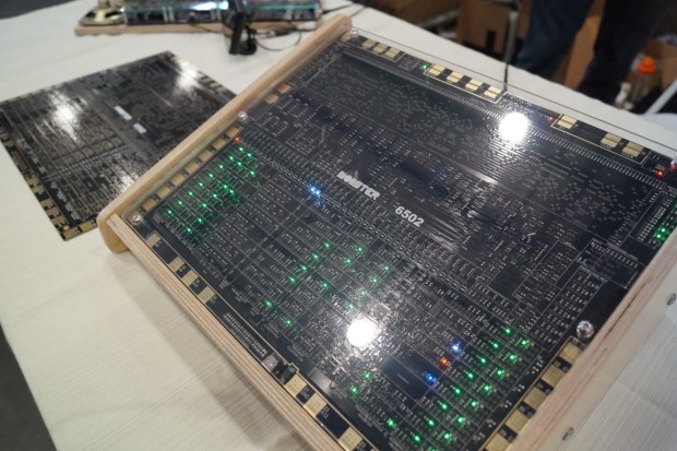
Breaking news! Eric Schlaepfer has just broken cover with his MOnSter 6502 project - using quad MOSFET surface mount transistors he was able to duplicate exactly the NMOS 6502 netlist as used in the simulator at visual6502.org - by using MOSFETs he avoided the pitfall of most low-level recreation attempts, which is coping with the bidirectional switches between the internal busses.
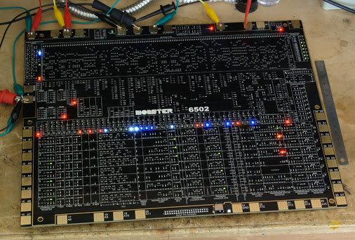
The starting point was to calculate the size of PCB - on estimating that it might be about a square foot, the project was on. There's more project timeline in the blog at
http://tubetime.us/?p=346
and a discussion on Hacker News at
https://news.ycombinator.com/item?id=11703596
Hat tip to +Kam-Yung Soh and +Samuel Falvo II
(We normally post weekly but this is a special occasion!)