6502.org Forum  Projects  Code  Documents  Tools  Forum
It is currently Fri Sep 20, 2024 11:43 am

All times are UTC


Post new topic Reply to topic  [ 4 posts ] 
Author Message
PostPosted: Wed Nov 11, 2015 2:20 pm 
Offline

Joined: Wed Nov 11, 2015 2:07 am
Posts: 1
Hello everyone!

I have been poring over the block diagram of the 6502 and I think I have a general understanding of things, but there are a few questions I still have:

(1) First of all, the various buses that run throughout the processor. I know that the labels on them were not given by the designer so they're kink of arbitrary, but they mostly seem to have names that makes sense: DB is used to transfer data to/from the data bus pins, ADL/ADH connect to the two pieces of the address bus. But SB left me a bit confused. I've decided that because it's connected to the output of the ALU maybe it means sum bus?

(2) Precharge and open drain mosfets. What does that mean? Do they serve a logical function, or are they only involved in providing power and ground (or something like that)?

(3) The pass mosfets between SB and DB (and also SB and ADH and maybe another one I missed), I think I understand. They are not transferring any data between the buses, but joining the buses together so that (while the pass mosfet is enabled) the two buses always have the same value, and will be required to only have one device between the two buses that is enabled?

(4) Is there any documentation on the random control logic? I've studied the instruction decoder, but this only gives arbitrary names to the 130 lines of the bus that connects it to the random control logic. I haven't been able to find any information on how the random control logic converts the 130 inputs to the 50 or so control lines.

(5) Another user on this forum gave a really good cycle by cycle breakdown of what happens when the processor executes LDA $4321. I understand how the clock signal is turned into a two-phase clock, so start and end of the cycle in BigEd's explanation, I assume, refer to phi-1 and phi-2. How does the processor synchronize with the "middle" of the cycle?

Thank you very much for any help :)


Top
 Profile  
Reply with quote  
PostPosted: Wed Nov 11, 2015 3:59 pm 
Offline
User avatar

Joined: Thu Dec 11, 2008 1:28 pm
Posts: 10938
Location: England
Hello, and welcome! It looks like I wrote that story back in 2009, and visual6502 wasn't released until 2010, so I didn't have the benefit of the illumination we got from visual6502 simulation. As you note, I didn't say anything about how the two clock phases are used. I spoke about beginning, middle and end because I think it helps to realise that things happen over time: the PC is not incremented instantaneously, but develops the PC+1 value over time. Some signals we look at come straight from latches right at the beginning of a clock phase, and some signals will be evolving during a clock phase and will only reach their final intended value right before the end of a phase, when a latch closes.

So if I were writing that story again, I might even write twice as many sections, distinguishing between the beginning, middle and end of each phase. (I'm not likely to do this!)

As it turns out, the random control logic includes quite a few latches, and indeed the control line drivers are also clocked, so there's a kind of pipelining going on in between the IR and the datapath, which isn't clear from the block diagram. You can follow it, if you're careful, on visual6502. You should look both at the tabulated signal values and the annotated layout.
http://visual6502.org/JSSim/expert.html ... f&steps=20

SB is the Special Bus - IIRC Donald Hanson actually visited MOS to see the blueprints and to draw up his block diagram, so probably most of the naming is in fact the naming that the designers would have used.

Precharge is used to drive the busses high, so that logic can conditionally drive them low. That turns out to be faster than allowing the logic to drive both ways. It might have some benefit in getting the high level to a higher voltage, I'm not sure. Given that the busses are precharged high, it means that a single pulldown transistor is all that's needed to drive it low if need be, so open drain outputs are all you need. No need for tristate drivers.

You are quite right that pass transistors don't have drive: they have very high or rather low resistance when on or off. So yes, they connect two busses so that, temporarily, they are logically one bus. And yes, the lone driver will be on one or the other, whereas a reader might be on the same half or the other half.


Top
 Profile  
Reply with quote  
PostPosted: Thu Nov 12, 2015 4:04 pm 
Offline
User avatar

Joined: Thu Dec 11, 2008 1:28 pm
Posts: 10938
Location: England
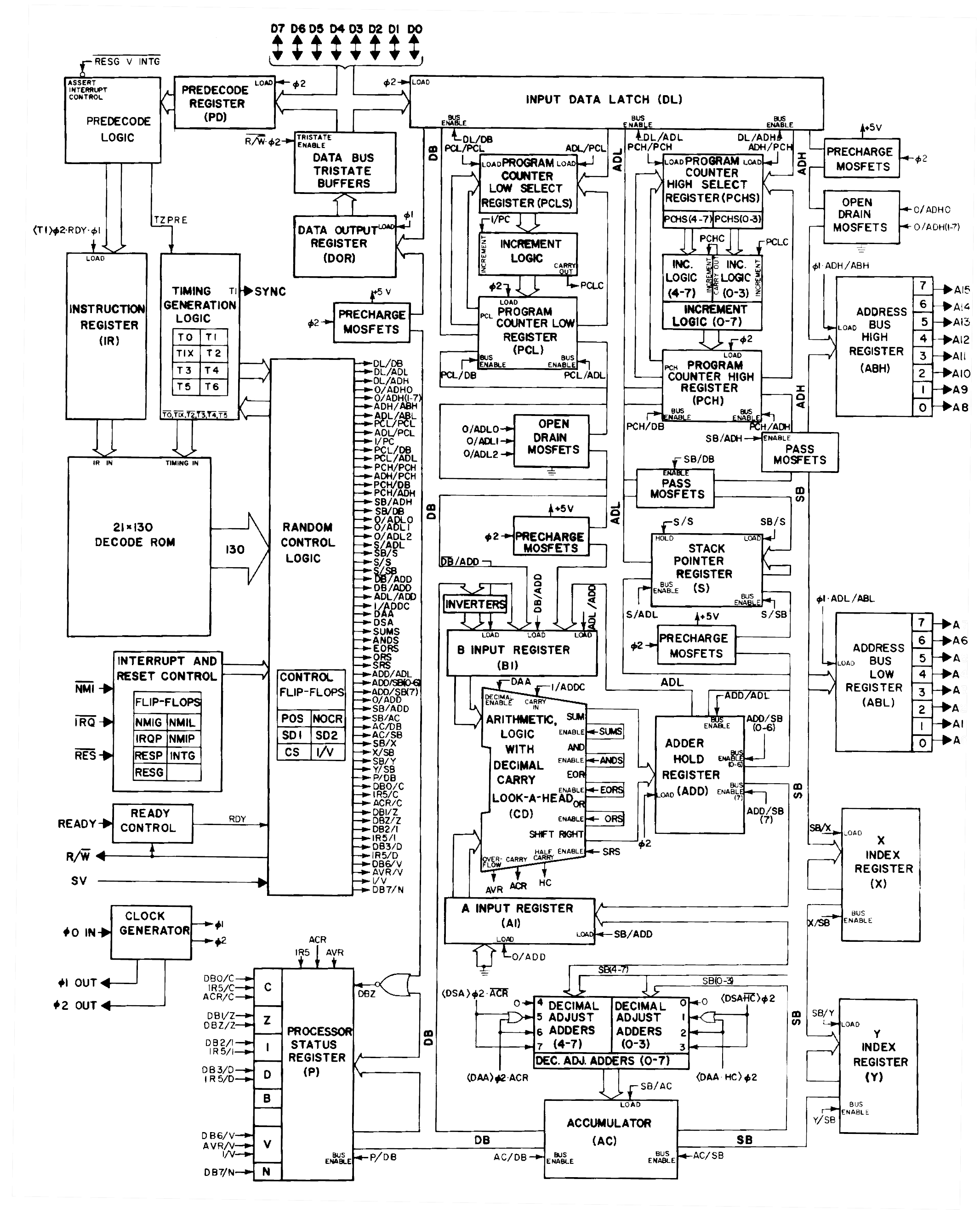
I missed a trick there - it's also very worthwhile to refer to Balazs' giant schematic, for example at
http://www.downloads.reactivemicro.com/ ... ematic.pdf

I looked for a simple worked example of tracing the workings of the random logic, and SB/X is simple. In the visual6502 you'll find this signal is called dpc3_SBX - because it's the 3rd datapath control signal from the left. In Balazs' schematic you'll find the signal is called R1x4 at the point of driving to the datapath, and 1x4 at the points of annotating the 8 transistors in the X register which control the writing of X from SB.

We can see from Balazs' schematic that the 8 pass gates which write to the 8 bits of X from the 8 bits of SB are driven by this one wire SB/X, and that wire is driven by a superbuffer. The wire is precharged with not-cp1, the superbuffer is driven by a pair of inverters, and their input is a latch clocked by cp2. The clock transistor for that latch is in the middle of this area:
http://www.visual6502.org/JSSim/expert. ... &zoom=10.4
and I've highlighted the two wires fore and aft.

If we now track North we find the gate which drives that signal - as Balazs found, it's a 3 input NOR, in the middle here:
http://www.visual6502.org/JSSim/expert. ... &zoom=10.0

Balazs named the three inputs 16,17,18 corresponding to those three columns of the decode PLA. He even labels them:
16: TAX, TSX, LDX #, zero, abs, zero,Y ,abs,Y
17: DEX
18: INX, NOP
In visual6502 we find these three are called
node: 985 op-T0-ldx/tax/tsx
node: 786 op-T+-dex
node: 1664 op-T+-inx
(Most names in visual6502 are from Segher's analysis, or Balazs' names, or names from the block diagram.)

We could in principle read off the pull-downs in the decode PLA to see which instructions and which T-states we expect these signals to be decoding.

Many of the visual6502 signals are not even named, but they do have unique node numbers. So dpc3_SBX is node 1186. You can find this out by clicking on it, and you can find the signal by highlighting it:
http://www.visual6502.org/JSSim/expert. ... d=dpc3_SBX
Actually more convenient is to check the sources where nodes are named, for example:
https://github.com/trebonian/visual6502 ... es.js#L871

It might be more convenient to load up two of the visual6502 source files in your editor. We can get them from the main website, or view them in github. In github we can link to individual lines, so let's do that.
Let's find the transistors which drive dpc3_SBX, and the transistors which drive those, and work backwards.

If we look for 1186 in
https://raw.githubusercontent.com/trebo ... segdefs.js
we find a '-' rather than a '+' - this means the node has no simple pullup to Vdd and therefore it's not the output of a simple logic gate. In fact it's the output of a superbuffer circuit, which has a faster pullup than a normal gate.

We can find the individual transistors in the transdefs file by looking for 1186 as a node number - we find 10 transistors, 8 are the pass gates which perform the write to X, one is the pullup and the other is the pulldown of the superbuffer. Here are those last two:
https://github.com/trebonian/visual6502 ... s.js#L2635
['t2633', 1247, 1186, 558, [1952, 1972, 4378, 4563],[186, 186, 15, 3, 3003] ],
['t2643', 625, 657, 1186, [1975, 1998, 4601, 4625],[23, 23, 24, 1, 571] ],

Here's one of the pass gates:
https://github.com/trebonian/visual6502 ... s.js#L1340
['t1338', 1186, 98, 1150, [2048, 2077, 3599, 3619],[29, 29, 20, 1, 564] ],
The thing to recognise here is that the first terminal, the gate, is the signal we want. Also that there are 8 transistors with this node as gate, which correspond to the 8 bits of X.

OK, I've slightly lost the plot now, so I'll post this - ask me to clarify or expand if you like!


Top
 Profile  
Reply with quote  
PostPosted: Sun Nov 29, 2015 6:32 pm 
Offline
User avatar

Joined: Thu Dec 11, 2008 1:28 pm
Posts: 10938
Location: England
Another reference work which might be useful or interesting, "org" here has annotated a 6502 die image with all the transistors, and also captured schematics for a lot of the chip:

Pointers to what looks like the final results of this reverse-engineering project:
https://commons.wikimedia.org/wiki/File ... S_6502.jpg [Transistor-annotated 6502 die image]
http://wiki.breaknes.com/ [in Russian]


Top
 Profile  
Reply with quote  
Display posts from previous:  Sort by  
Post new topic Reply to topic  [ 4 posts ] 

All times are UTC


Who is online

Users browsing this forum: No registered users and 108 guests


You cannot post new topics in this forum
You cannot reply to topics in this forum
You cannot edit your posts in this forum
You cannot delete your posts in this forum
You cannot post attachments in this forum

Search for:
Jump to: