banedon wrote:
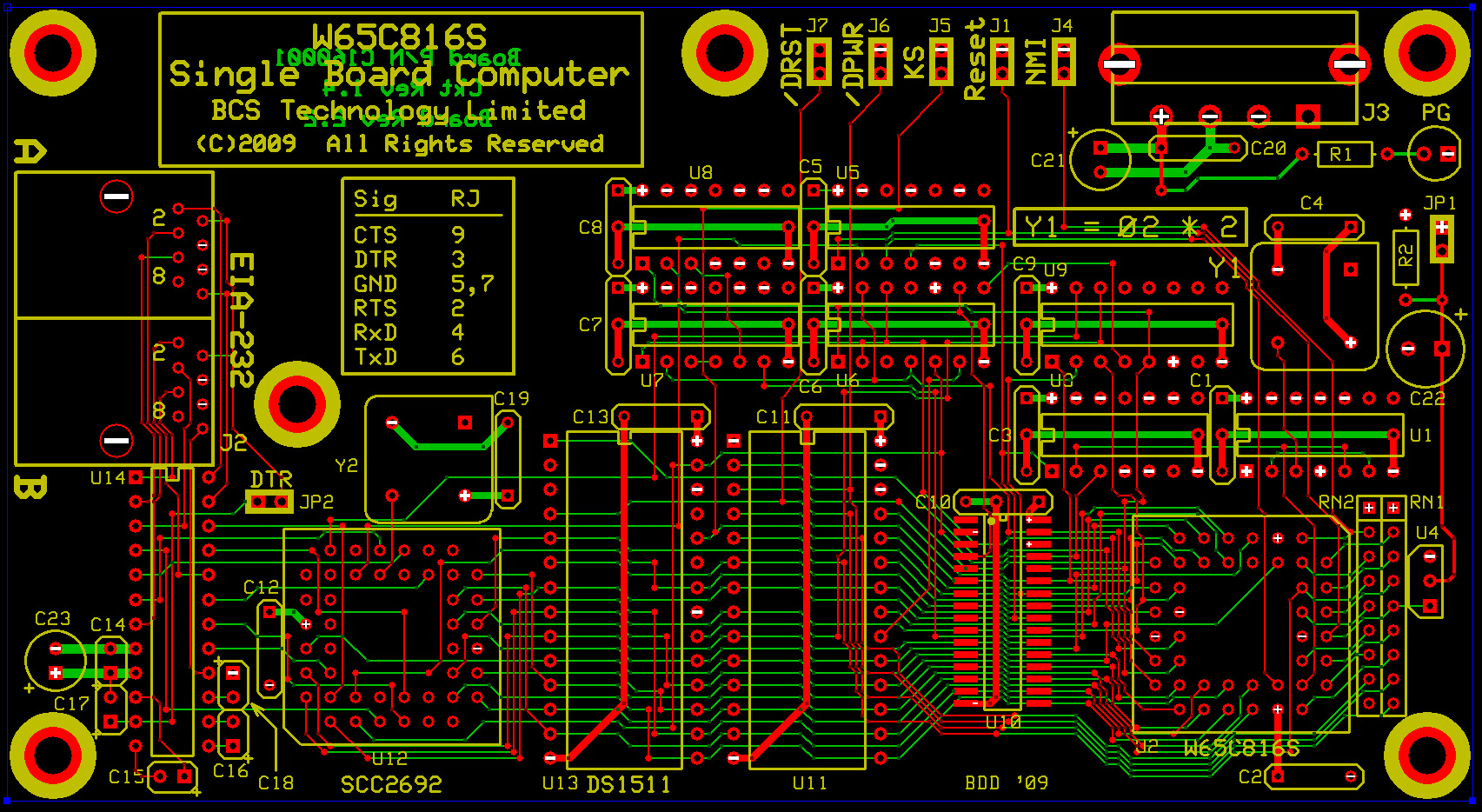
I've asked about this previously and have set up a star ground and power using wire wrap. However, I'm now working on my first PCB based 65C02 design and want to be absolutely sure of how to implement this using a 4 layer board.
The PCB is going to be layered thus:
Top layer - signals
2nd layer - GND plane
3rd layer - Power/+5V plane
Bottom layer - signals
To make the power and GND planes into star one would I then divide those planes into sections something along the lines of this? The brown lines represent breaks in the copper.
My opinion is that such an arrangement has no value and may actually give rise to some issues.
The value of the inner layers as power and ground planes is that they are essentially uninterrupted. Hence the ESR of these layers is vanishingly small, which means that ground bounce and local Vcc fluctuations are largely eliminated. Also, the combination of the two layers acts like a sizable bypass capacitor, which can do quite a bit in keeping circuit noise to a minimum.
In my POC units, I did nothing to change the topology of the inner layers. Here's what the ground layer looks like in EPCB:
Attachment:
File comment: POC V1.1 Ground PLane
 ground_plane.gif [ 63.53 KiB | Viewed 1472 times ]
Other than where holes and via pass through, there are no interruptions. This circuit is dead quiet.
Attachment:
File comment: Power Distribution to Chip
 vcc_distribution.gif [ 38.04 KiB | Viewed 1472 times ]
The above shows how I bring Vcc to devices. The theory is that any noise that is emitted out of the Vcc pin by the device is seen by the device's bypass capacitor before it gets to the inner power plane. The connection between device and capacitor is short and thick, which reduces the ESR to essentially zero. This practice is based upon recommendations by Dr. Howard Johnson, generally acknowledged to be
the guru on this sort of stuff.


