6502.org Forum  Projects  Code  Documents  Tools  Forum
It is currently Sun Apr 28, 2024 11:16 am

All times are UTC


Post new topic Reply to topic  [ 558 posts ]  Go to page Previous  1 ... 11, 12, 13, 14, 15, 16, 17 ... 38  Next
Author Message
 Post subject: Re: TTL 6502 Here I come
PostPosted: Tue Mar 14, 2017 6:56 pm 
Offline
User avatar

Joined: Tue Nov 16, 2010 8:00 am
Posts: 2353
Location: Gouda, The Netherlands
Looking good!


Top
 Profile  
Reply with quote  
 Post subject: Re: TTL 6502 Here I come
PostPosted: Wed Mar 15, 2017 1:12 pm 
Offline
User avatar

Joined: Mon May 25, 2015 2:25 pm
Posts: 632
Location: Gillies, Ontario, Canada
I can't wait to see it all working... it has been great to follow the progression.
When I finish my current project, I intend to do a 7400 based CPU as well, and your build has been inspiring as well as educational.
Thanks for the spark!

Brad


Top
 Profile  
Reply with quote  
 Post subject: Re: TTL 6502 Here I come
PostPosted: Fri Mar 17, 2017 9:26 pm 
Offline
User avatar

Joined: Sun Oct 18, 2015 11:02 pm
Posts: 428
Location: Toronto, ON
Thanks for the encouragement gents! Feels great to be making progress.

Brad, very cool that you are considering a TTL CPU build. Will definitely be interesting to see where you take that!

I've been making up BOMs and thinking a bit about a basic test rig to bring up the CPU. Initially, probably just some RAM and a step clock will do. This cheap and cheerful EPROM programmer works for the microcode ROMs, but I can also use to transfer a code image onto NVRAM via USB - nice and simple. Down the road a bit, I expect I'll need to build an SBC to test more thoroughly; probably something like Daryl's SBC 2. I thought that would make a great first home for the TTL CPU. I might even make it as another "optional" card on the CPU itself, which would make for a nice package - we'll see. Of course, the idea is that eventually the CPU will use a ribbon cable and socket adaptor to plug directly into any NMOS or CMOS 6502 host, including a VIC20 or C64.

As ever, lots of work to do, but I'm now looking forward to some soldering :shock:

Drass

_________________
C74-6502 Website: https://c74project.com


Top
 Profile  
Reply with quote  
 Post subject: Re: TTL 6502 Here I come
PostPosted: Mon Apr 10, 2017 1:43 am 
Offline
User avatar

Joined: Sun Oct 18, 2015 11:02 pm
Posts: 428
Location: Toronto, ON
Once in a while I feel a little "in over my head" on this project - like right now, for instance. Some parts arrived, and ... good Lord! It's easy to forget how truly tiny an 0603 capacitor is, especially after staring at a large screen for months. Getting an iron between bypass cap and IC pad is going to be very interesting in more than a few places. And there are hundreds of parts and thousands of solder points on these boards!

Well, after my heart-rate came down a bit, I got back to work :)
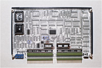
. I printed off scale images of the boards, and, tweezers in hand, I placed a few components - I could easily see various problems. I've circled in red a couple of examples on the pic below, and circled in blue some smaller components that are easy to miss:
Attachment:
Card A Mockup Marked.jpg
Card A Mockup Marked.jpg [ 550.95 KiB | Viewed 1328 times ]
One issue is that some vias are really quite close to adjacent pads. After Dieter alerted me to it, I opted for covering vias with solder mask to prevent solder bridges. Then I noticed I had a few caps placed WITHIN the outlines of ICs! Silly, but I had the silkscreen layer off when I was placing the caps and just missed it in a few instances. I also underestimated the clearance needed around through-hole IC sockets, and the spacing between bypass caps and nearby pads - it's is just too tight in places. After careful inspection, I think I've spotted most of the trouble spots and will get busy sorting them out as best I can.

Oh, and I also ordered the wrong parts for the inter-card connectors (the pins are too short to reach between the cards :roll:). Aside from that, I'm quite happy really. Considering the many things that could be wrong, it's remarkable that so much is ok. As to how to manage the soldering in really tight spots, well, that remains a mystery. Perhaps solder paste and a heat gun might be the answer, but I guess we'll see how the iron works out first.

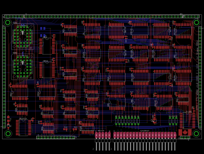
In the meantime, I did a little research on PCB manufacture and discovered "panelizing". Turns out I can put four Eurocards on a single panel and get them made for about the same price as a single card! That's a big deal, and a strong incentive to get the other PCBs done (a good idea anyways just to make sure I don't have any surprises later). Laying out the K24 card was bound to be much easier that the others so I just went for it:
Attachment:
Card C-K24 Brd.png
Card C-K24 Brd.png [ 62.6 KiB | Viewed 1328 times ]
Note the pinout header at bottom for the ADX bus (K24 extended address bus A16..24) and the SPI interface (which follows Garth's SPI-10 spec :D). The K24 microcode has a custom SPI opcode which should enable the TTL CPU to connect directly to an SPI Mode 3 device on this header.

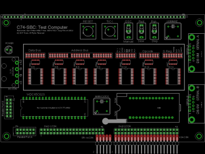
I also decided to try to get a test harness SBC done so I could include it on the PCB panel (the initial testing of the TTL CPU will be with just a memory chip on a breadboard but I'll need an SBC thereafter):
Attachment:
Card D-SBC Brd.png
Card D-SBC Brd.png [ 24.05 KiB | Viewed 1328 times ]
I used Garth's 6502 Primer, Daryl's SBC2 and BDD's POC1 as references here, so the design will look very familiar. The SBC uses a simple variation of Garth's address decoder, an NXP SCC2692 UART per BDD's recommendation, and a WDC65C22 VIA for a nice complement of interrupt sources for testing. I used a 128K RAM chip so the K24 extended address bus can be exercised, and also put the ROM on a ZIF socket to make it easy to re-program. I included a socketed WDC65C02 on the board to let me verify the SBC itself. I can then remove the MPU from it's socket and stack the card on the TLL CPU for testing. Incidentally, I added a wait-state when the SBC accesses peripherals (only when using the FAST clock) so that I can try to run the TTL CPU flat-out and see what happens :mrgreen:. One neat thing is I had some fun implementing the TTL CPU's AUX control signal to switch between FAST and SLOW clocks on the fly. And, of course, I added lots of blinking lights (including some for CPU-internal signals, which will be handy). I'll share the schematics for the SBC shortly.

Ok, that's it for now. Back to those tiny caps :)

Cheers,
Drass

_________________
C74-6502 Website: https://c74project.com


Top
 Profile  
Reply with quote  
 Post subject: Re: TTL 6502 Here I come
PostPosted: Mon Apr 10, 2017 5:07 am 
Offline
User avatar

Joined: Tue Nov 16, 2010 8:00 am
Posts: 2353
Location: Gouda, The Netherlands
Drass wrote:
It's easy to forget how truly tiny an 0603 capacitor is

There's an easy solution for that. Try working with 0402 for a few days, and then 0603 will look like a house brick.

Quote:
I also underestimated the clearance needed around through-hole IC sockets, and the spacing between bypass caps and nearby pads

Put the components in first, and then you can solder the caps on top of the leads. And in really tight places, just leave out the bypass caps.


Top
 Profile  
Reply with quote  
 Post subject: Re: TTL 6502 Here I come
PostPosted: Mon Apr 10, 2017 8:22 pm 
Offline
User avatar

Joined: Wed Mar 01, 2017 8:54 pm
Posts: 660
Location: North-Germany
Drass wrote:
...
I also underestimated the clearance needed around through-hole IC sockets, and the spacing between bypass caps and nearby pads - it's is just too tight in places.
...

Perhaps pin carriers may help you:
https://www.mpe-connector.de/file_db/fa ... et/074.pdf

If your pin holes are wide enough this is also possible:
https://www.mpe-connector.de/file_db/fa ... et/077.pdf

Of course there are more vendors.


Top
 Profile  
Reply with quote  
 Post subject: Re: TTL 6502 Here I come
PostPosted: Tue Apr 11, 2017 6:05 am 
Offline
User avatar

Joined: Fri Nov 09, 2012 5:54 pm
Posts: 1392
Placing components below IC sockets has its pros and cons.

Some years ago, I had a PCB that failed after some hours of operation.

It turned out, that somebody had soldered a 100nF capacitor instead of a pullup resistor.
It was tied to the /RESET input of some 74HC595 chips.

The weak input current of the CMOS inputs slowly charged the capacitor after power_up,
and after some hours of operation the /RESET signal reached logic LOW level.

Just to be able to _see_ that tiny SMD part that caused the trouble
I had to cut off a bit of that precision DIP socket...


Top
 Profile  
Reply with quote  
 Post subject: Re: TTL 6502 Here I come
PostPosted: Thu Apr 13, 2017 1:57 am 
Offline
User avatar

Joined: Sun Oct 18, 2015 11:02 pm
Posts: 428
Location: Toronto, ON
Great suggestions gents, thank you. (although I'm not about to try 0402 caps at this stage of the game :mrgreen:)

I think I've managed to address most of the issues by nudging the caps around a bit. I have as much solder mask now between caps and pads as there is between the pads themselves, and I've tried to moved the caps away from the body of any ICs. Ironically, there was room in most cases, but I was just not considering the physical scale when placing the parts. (If it passed the DRC, that was good enough!) Glad I made those paper mockups. But I don't think I'll make one for the K24 card. Spacing there is quite generous, and there are no new footprints to worry about.

So that leaves the SBC ... here are some draft schematics:
Attachment:
Card D-SBC Sch p1.png
Card D-SBC Sch p1.png [ 34.34 KiB | Viewed 1207 times ]

Attachment:
Card D-SBC Sch p2.png
Card D-SBC Sch p2.png [ 27.29 KiB | Viewed 1207 times ]

Attachment:
Card D-SBC Sch p3.png
Card D-SBC Sch p3.png [ 31.02 KiB | Viewed 1207 times ]

Attachment:
Card D-SBC Sch p4.png
Card D-SBC Sch p4.png [ 24.41 KiB | Viewed 1207 times ]

Attachment:
Card D-SBC Sch p5.png
Card D-SBC Sch p5.png [ 26.04 KiB | Viewed 1207 times ]

As I described, the idea is that the SBC sits on top of the TTL CPU, and connects directly to the pinout headers on the Registers Card. I checked the pin heights and it all fits with the cards 12mm to 13mm apart and a female connector on the underside of the SBC.

The memory map on the SBC is as follows:

$010000 - $01FFFF RAM
$00C000 - $00FFFF ROM
$00A000 - $00BFFF IO - 6522 VIA
$008000 - $009FFF IO - 2692 UART
$000000 - $007FFF RAM

The extra RAM is only be available to the TTL CPU, but I can test everything else with the socketed WDC 65C02. The address decoder is only 1 gate deep for RAM and 3 gates deep for ROM and peripherals, which is nice. I validated the rather convoluted clocking circuit, which includes FAST, SLOW, STEP (Single-instruction), and TICK (single-cycle) - a little much, I agree, but it was fun to do it :). (It was a bit tricky to synchronize everything so no partial cycles are generated, but I think got that sorted out). The TICK push-button does double duty, executing a single cycle in MANUAL mode (using Garth's Pulse generator from the 6502 primer), but also releasing RDY to execute a single instruction when in STEP mode. Incidentally, the "Gate-Switch-Debouncers" are Dieter's idea, and they worked out very nicely given that I had spare gates on the board already!

Of course, I would very much appreciate any thoughts or suggestions on the SBC (or otherwise).

Cheers!

_________________
C74-6502 Website: https://c74project.com


Top
 Profile  
Reply with quote  
 Post subject: Re: TTL 6502 Here I come
PostPosted: Thu Apr 13, 2017 6:08 am 
Offline
User avatar

Joined: Fri Nov 09, 2012 5:54 pm
Posts: 1392
Now some comments on your SBC schematics:

;---

On the W65C02, BE is high_active, not low_active like in your schematics.
You connected BE with a pull_down resistor to GND, what would disable the bus of the W65C02 by default.

Please check.

;---

IC5A, a 7414 inverter, is wired up as a switch debouncer.
Sorry, this won't work.
You either need to use a non_inverting gate there, or to put two inverters in a row.

// Might be possible to turn that spare 7474 flipflop into a RS flipflop and to use it as a debouncer.

Please check.

;---

IC7C, the OR gate that generates /RAM.SEL, looks wrong. IMHO this should be an AND gate.
/816BNKH is high, when the CPU accesses $00xxxx.
An OR gate there would select the RAM for $010000..$017FFF, $020000..$027FFF and so on.
But the RAM won't be selected for $000000..$007FFF !

Please check.

Edit: R13, that pulldown resistor for the /816BNKH signal...
would be better to make this a pullup resistor.

Please check this, too.

;---

Now for the LEDs: 7*8 = 56 LEDs.
If they all are on, and if we could expect something like 10mA per LED, this would be 560mA in total.
Would be good to add a switch (or a jumper) for disabling all the LEDs.
Just tie the /G inputs of all the LED drivers together, and add a pullup resistor and a switch\jumper to GND.

// When I had built my experimental TTL 65xx peripherals, I did something like this because I was using
// only a humble 2A voltage regulator, which sometimes wasn't up to the task...

Please check.

;---

Feels like we are almost there.
Go, Drass, go. :)


Top
 Profile  
Reply with quote  
 Post subject: Re: TTL 6502 Here I come
PostPosted: Thu Apr 13, 2017 1:05 pm 
Offline
User avatar

Joined: Fri Dec 11, 2009 3:50 pm
Posts: 3346
Location: Ontario, Canada
ttlworks wrote:
Feels like we are almost there.
Go, Drass, go. :)

Yes, indeed! :)

BTW Dieter mentioned 10 mA per LED, but with modern, high-brightness LED's that's probably quite a lot more than necessary. You might want to use a socket for the resistor array so you can easily change the value.

cheers,
Jeff


Attachments:
excerpt.png
excerpt.png [ 6.36 KiB | Viewed 1159 times ]

_________________
In 1988 my 65C02 got six new registers and 44 new full-speed instructions!
https://laughtonelectronics.com/Arcana/ ... mmary.html
Top
 Profile  
Reply with quote  
 Post subject: Re: TTL 6502 Here I come
PostPosted: Sat Apr 15, 2017 4:34 pm 
Offline
User avatar

Joined: Sun Oct 18, 2015 11:02 pm
Posts: 428
Location: Toronto, ON
Thanks for these comments! Very helpful.

ttlworks wrote:
On the W65C02, BE is high_active
Some misconceptions die hard - Garth pointed this out as well in response to my very first post on this thread! ... :oops:

Quote:
IC5A, a 7414 inverter, is wired up as a switch debouncer. Sorry, this won't work.
Looks like I made a "bouncer" instead of a debouncer :roll:

Quote:
IC7C, the OR gate that generates /RAM.SEL, looks wrong. IMHO this should be an AND gate.
Agreed. Happily, there is a spare AND gate on the board. The OR can go to the debouncer.

Quote:
Edit: R13, that pulldown resistor for the /816BNKH signal...
Great catch! Boy, that's a confusing name for that signal: "/816 Bank HIGH" is LOW when the Bank is HIGH. Positive logic "816BNK0" is probably better.

Quote:
tie the /G inputs of all the LED drivers together, and add a pullup resistor and a switch\jumper to GND.
Good idea. I suspect I will also appreciate being able to turn off the LED panel when not in use!

Dr Jefyll wrote:
You might want to use a socket for the resistor array so you can easily change the value.
Good point ... but rather than sockets, I think I'll try the LEDs out on a test board before settling on a value for the final PCB.

Quote:
Go, Drass, go. :)
This always makes me smile ... many thanks for the help and encouragement! We're almost there :)

Cheers.

_________________
C74-6502 Website: https://c74project.com


Top
 Profile  
Reply with quote  
 Post subject: Re: TTL 6502 Here I come
PostPosted: Tue Apr 18, 2017 7:12 am 
Offline
User avatar

Joined: Fri Nov 09, 2012 5:54 pm
Posts: 1392
Drass wrote:
Positive logic "816BNK0" is probably better.

I agree.

Drass wrote:
This always makes me smile ... many thanks for the help and encouragement!

You are welcome. To me, it sure is a new and exciting experience to be just "the project manager". :)


While taking another look at your schematics, I noticed a pulldown resistor (R10) for the /816MODE signal.
If K24 won't be installed, /816MODE would be low, and I think it's supposed to be high instead...
because the "816 mode" simply won't work without the K24 PCB.

Please check polarity and pullup\pulldown for this signal.

Hmm... since we are at it, please check the AUX signal, too...
We reserved that AUX signal for switching between slow and fast CPU clock by software later,
and for maintaining C64 compatibility the CPU is supposed to end up in "slow mode" after a hardware reset.
The reason is, that an unmodified C64 kernal might have problems to communicate with a 1541 floppy drive when the CPU is in "fast mode".

BTW: you are using a 128kB RAM, the SBC doesn't seem to make use of A23..A17.
So if you should be running out of PCB space, replacing the resistor network <24-DWN with a pulldown resistor
for A16 only might be an option.


Top
 Profile  
Reply with quote  
 Post subject: Re: TTL 6502 Here I come
PostPosted: Tue Apr 18, 2017 7:19 am 
Offline
User avatar

Joined: Fri Nov 09, 2012 5:54 pm
Posts: 1392
Felt a need to clarify, how my switch debouncer works.

Attachment:
debounce.png
debounce.png [ 5.73 KiB | Viewed 1037 times ]


If a SPDT switch bounces, it either bounces between low and open, or between high and open.

If the switch is open, the resistor works either as a pullup or a pulldown for the input of the gate,
to make the non_inverting logic gate keep its logic level at the output.

To change the logic level at the gate output, some current has to flow through the resistor.

470 Ohm sure is a little bit low, but it increases reliability of the circuit,
and current only flows for a short moment when the output of the logic gate changes.

74HC\74AC would be best for this application, since the logic level threshold is half the supply voltage.
74HCT\74ACT might work too, but at a logic level threshold of ca. 1.3V the noise immunity probably would be less good.

74LS won't work too well in this application, requiring a lower resistor value bacause of the 1..2mA input current
of a TTL LS gate when pulling the input low...
LS logic level threshold is ca. 1.3V, and the output voltage of the LS gate sure would be a little bit more than 0V.

Nice thing is, that one could debounce 8 SPDT switches with a 74HC245 or 74HC541 plus 8 resistors.
No Schmitt-Trigger required.

;---

BTW:
Actually, the circuit is derived from a form of "low_power" active bus termination.
Imagine to have the non_inverting logic gate tied with the input to a data bus line,
and a termination resistor between input and output of the gate...

While looking at Alsi's SBC schematics some time ago, it felt like there had to be a better way of debouncing switches,
and this thought had circled around in my backhead for a while.
It took me some time to realize that this sort of active bus termination could be used as a switch debouncer,
so the idea came a bit too late for Alsi's project, sorry.


Top
 Profile  
Reply with quote  
 Post subject: Re: TTL 6502 Here I come
PostPosted: Thu Apr 20, 2017 1:55 am 
Offline
User avatar

Joined: Sun Oct 18, 2015 11:02 pm
Posts: 428
Location: Toronto, ON
Quote:
If K24 won't be installed, /816MODE would be low, and I think it's supposed to be high instead...
/816MODE is not used by the SBC so it's not critical one way or the other. Actually, it might be interesting to come up with a creatve use for this signal: /816MODE is low when the 65816 microcode is selected. Perhaps the SBC can reconfigure the memory map on the fly whenever the 65816 instruction set is active? Or maybe some sort of "privileged" mode operation? Not sure.

Quote:
please check the AUX signal, too.
The AUX bit is cleared on RESET by the K24 hardware. The SBC as currently set up will therefore come up in SLOW mode. Of course, logic external to the CPU is free to interpret AUX anyway it chooses, for clock management or otherwise ...

Quote:
So if you should be running out of PCB space, replacing the resistor network <24-DWN with a pulldown resistor
for A16 only might be an option.
I'll be laying out the SBC shortly so I'll keep this in mind. Thanks for mentioning it.

_________________
C74-6502 Website: https://c74project.com


Top
 Profile  
Reply with quote  
 Post subject: Re: TTL 6502 Here I come
PostPosted: Mon May 01, 2017 1:48 am 
Offline
User avatar

Joined: Sun Oct 18, 2015 11:02 pm
Posts: 428
Location: Toronto, ON
I made a little "pre-manufacturing checklist" for the PCBs, which included a final "visual check" of the schematics. I have to confess it seemed almost pedantic to be checking schematics again at this late stage, but, wouldn't you know it, I found a problem on the ALU Board! :shock: Somehow I managed to reverse a couple of pins on a 74AC257. Looking back at an older schematic, I can confirm absolutely that the connections were made correctly before. And yet, inexplicably, here they are - wrong in the version I routed! Argh! :twisted: It took quite some effort to re-work the relevant tracks, but of course it sure beats having to redo a board for such a silly error. I'm bracing for some heavy debugging once the CPU is built.

On another note, I had a chance to route the SBC:
Attachment:
Card D-SBC Brd.png
Card D-SBC Brd.png [ 68.88 KiB | Viewed 899 times ]
Comparatively, there was lots of space on this board. I put the glue and I/O ICs on the back, and left the upper portion of the pcb open for through-hole switches and pushbuttons. I'm still pondering some late changes, but either way, a paper mockup sure seems like a good idea on this one - just to check all the new footprints. Incidentally, I found a way to print a nice "assembly guide" for each board from Eagle to help during soldering. Here is the ALU & CU Card top-side:
Attachment:
Card B-ALU & CU Assembly.png
Card B-ALU & CU Assembly.png [ 24.5 KiB | Viewed 899 times ]

With the boards getting closer now, I spent some time looking into manufacturing and panelization. It looks like pcbway.com will put all four cards into a single V-Scored panel - that would be great! They support 4 mil tracks, 4 mil spacing and 2mm drills, which actually exceeds the requirements of these boards. I've yet to confirm all the specs, but it seems they might work out. I would be curious to know if anyone here has used them in the past, or whether another manufacturer might be better in this instance.

Speaking of panels, there are a number of scripts and other solutions out there for merging multiple gerbers together - all of which I've yet to investigate fully. I'll report back once I've had a good look. Unfortunately, my version of Eagle restricts the pcb dimensions, so I do need to find an alternative. The fallback, of course, is to get the boards made separately (although at a significantly higher price). We'll see.

Cheers for now!

_________________
C74-6502 Website: https://c74project.com


Top
 Profile  
Reply with quote  
Display posts from previous:  Sort by  
Post new topic Reply to topic  [ 558 posts ]  Go to page Previous  1 ... 11, 12, 13, 14, 15, 16, 17 ... 38  Next

All times are UTC


Who is online

Users browsing this forum: No registered users and 34 guests


You cannot post new topics in this forum
You cannot reply to topics in this forum
You cannot edit your posts in this forum
You cannot delete your posts in this forum
You cannot post attachments in this forum

Search for:
Jump to: