6502.org Forum  Projects  Code  Documents  Tools  Forum
It is currently Thu May 02, 2024 2:19 pm

All times are UTC


Post new topic Reply to topic  [ 558 posts ]  Go to page Previous  1, 2, 3, 4, 5, 6, 7, 8 ... 38  Next
Author Message
 Post subject: Re: TTL 6502 Here I come
PostPosted: Mon Nov 09, 2015 10:41 pm 
Offline
User avatar

Joined: Sun Oct 18, 2015 11:02 pm
Posts: 428
Location: Toronto, ON
Arlet wrote:
It's still authentic because the original 6502 designers didn't implement illegal opcodes either. They just happened to do something.
I like that perspective ... replicate what was implemented on purpose but not necessarily the accidental byproducts. Nice summary.

_________________
C74-6502 Website: https://c74project.com


Top
 Profile  
Reply with quote  
 Post subject: Re: TTL 6502 Here I come
PostPosted: Sat Nov 14, 2015 5:33 am 
Offline
User avatar

Joined: Sun Oct 18, 2015 11:02 pm
Posts: 428
Location: Toronto, ON
Firstly, thanks to all for all the thoughtful suggestions I have been receiving via PMs. Folks have been incredibly generous with their time and knowledge and I am benefiting from a wonderful fast-paced education. Please feel free to comment directly on the thread or PM me if that is more comfortable. Either way, I'll try to get all the information posted as we go.

It's been a busy week with little time for the project, so I hope to get caught up this weekend. There are lot's of improvements still to make on the ALU schematics, but I wanted to post the Registers schematic which now includes some great refinements. I am really enjoying learning about these optimizations so I hope they are of value to others as well.

  • As suggested by Dr Jefyll: I removed 74541 buffers connecting the S and T registers to the R and A Busses. Instead, the registers are duplicated so two copies of each exist, one dedicated to each of the buses in turn. This reduces the package count and the propagation delay through the circuit at the same time. Love that :)
  • As suggested by Dr Jefyll: I replaced the 74574 used for IR with a 74273. The latter sports a Clear input signal and so I could dispense with the additional 74541 used to generate a zero value. The INT signal is now connected directly to the Asynchronous Clear pin and the effect is equivalent. In order to protect against glitches, the INT signal had to be routed through a latch like other write signals. That is done along with other logic on the ALU card.
  • As suggested by ttlworks: The latching of write signals was awkward in that I was triggering the latch on the leading-edge of phase2 so the WR signals still had to be gated with the clock (to delay them until the trailing-endge of phase2). Instead, I now latch the signals with a 74273 (with the Async Clear signal) on the trailing edge of phase2 and clear the latch on the leading edge of phase2 to prepare it for the next cycle. This delivers the WR signals to the registers at the right time and glitch-free as well. This is one of those "what was I thinking" moments when you look back and realize how awkward a previous solution was. It's very satisfying to clean it up. A final detail is that I had to invert the polarity of the WR signals so they were all active high. The net result is gating is no longer required at all and I can finally dispense with the 10 NOR gates used for that purpose.
  • I also used the spare 74139 decoder (the pair of INC.MX) to replaced a bunch of gates in front of the ADH and ADHS 74541 buffers. This cleans things up a bit and again eliminates the more unnecessary gates.

I'll also mention that the invalid INC16 Carry Look Ahead logic for 16 bit decrement operations did not escape notice. 16 bit decrement operations in fact do not work correctly. As it turns out, this is ok because all decrement operations required by the microcode are only 8 bits (e.g. when decrementing SP) and the invalid look-ahead carry is safely ignored in that case.

Beyond that, I would still like to eliminate the CONST0 74541 used to generate a zero value on the R Bus. I've decided to postpone doing this until the interrupt processing sequences are finalized since they use many of the constants and other optimizations may arise in the process.

One other potential improvement I am exploring concerns the MUXes in front of PCL/DPL and PCH/DPH and looking for ways to reduce the package count further. One suggestion was to try using a 74LS298 muxes which have a 4 bit register built-in. I'll study up on the weekend and take a closer look at this.

Once again, I'm loving the learning process and very appreciative of all the help.

The new version of the schematic is attached.

Cheers!


Attachments:
Card A-Registers.png
Card A-Registers.png [ 300.82 KiB | Viewed 3580 times ]

_________________
C74-6502 Website: https://c74project.com
Top
 Profile  
Reply with quote  
 Post subject: Re: TTL 6502 Here I come
PostPosted: Sat Nov 14, 2015 8:57 am 
Offline
User avatar

Joined: Thu Dec 11, 2008 1:28 pm
Posts: 10793
Location: England
It's great when things get simpler and better at the same time!


Top
 Profile  
Reply with quote  
 Post subject: Re: TTL 6502 Here I come
PostPosted: Sat Nov 14, 2015 4:25 pm 
Offline
User avatar

Joined: Sun Jun 30, 2013 10:26 pm
Posts: 1927
Location: Sacramento, CA, USA
I have never met Jeff and Dieter in person, but they seem to be great guys, in addition to their awesome hardware chops!

Best wishes,

Mike B.


Top
 Profile  
Reply with quote  
 Post subject: Re: TTL 6502 Here I come
PostPosted: Sun Nov 15, 2015 11:11 pm 
Offline
User avatar

Joined: Sun Oct 18, 2015 11:02 pm
Posts: 428
Location: Toronto, ON
barrym95838 wrote:
I have never met Jeff and Dieter in person, but they seem to be great guys, in addition to their awesome hardware chops!

Best wishes,

Mike B.

As the beneficiary of a lot of that goodwill and skill, I have to agree wholeheartedly!

One quick question while I'm here: I've been spending some time redoing the mechanism for handling interrupts and just want to confirm the behaviour of the B flag. I have implemented the following:
http://visual6502.org/wiki/index.php?title=6502_BRK_and_B_bit
Quote:
First technical point: the B flag position in the status register is not a bit in the status register: it is unaffected by PLP and RTI. However, the 6502 does push the register with either a 1 or 0. The intention is to distinguish a BRK from an IRQ, which is needed because these two share the same vector. Brad Taylor says:
software instructions BRK & PHP will push the B flag as being 1.
hardware interrupts IRQ & NMI will push the B flag as being 0.

The question revolves around what PHP should do. Testing a couple of emulators, I see PHP push 1 for the B flag when used within the BRK service routine but 0 otherwise. On the other hand, so far as I can tell, the Visual 6502 pushes a 1 for the B flag on a PHP outside a BRK. The Wiki page indicates there are some "bugs" with this as well so I'm somewhat at a loss as to what the correct behaviour is. I suspect for all practical purposes the rules on the Wiki are accurate. Please let me know if that's not the case.

Thanks!

_________________
C74-6502 Website: https://c74project.com


Top
 Profile  
Reply with quote  
 Post subject: Re: TTL 6502 Here I come
PostPosted: Mon Nov 16, 2015 12:37 am 
Offline
User avatar

Joined: Sun Jun 30, 2013 10:26 pm
Posts: 1927
Location: Sacramento, CA, USA
As far as I can tell, PHP always pushes 1s for bits 4 and 5. I don't think the 6502 has any way of "knowing" that it's within a BRK service routine ... that's the firmware's job.

Mike B.


Top
 Profile  
Reply with quote  
 Post subject: Re: TTL 6502 Here I come
PostPosted: Mon Nov 16, 2015 4:27 am 
Offline
User avatar

Joined: Sun Oct 18, 2015 11:02 pm
Posts: 428
Location: Toronto, ON
Thanks Mike. That makes sense. I'll stick to that implementation.

Well, what a weekend! Substantial revisions to the ALU, complete overhaul of interrupt handling, several efficiency improvements and lots of general clean-up. I believe the changes have made for a very material performance improvement and certainly for a much simpler implementation. Very exciting! Unfortunately I did not get a chance to review adequately before the end of the weekend. I am reluctant to post a new rev given this state of affairs. The week will be very busy otherwise so it will be until next weekend before I get much more done. In the meantime, best regards to all here.

Cheers!

_________________
C74-6502 Website: https://c74project.com


Top
 Profile  
Reply with quote  
 Post subject: Re: TTL 6502 Here I come
PostPosted: Tue Nov 24, 2015 4:37 am 
Offline
User avatar

Joined: Sun Oct 18, 2015 11:02 pm
Posts: 428
Location: Toronto, ON
Another productive weekend!

I’m very excited about where things are on the project. Most of the work at this stage is on refining the working model, and I could not be happier with the improvements. The package count is dropping and the circuits are getting simpler and faster at the same time - awesome!

A rich-source of improvements came as a result of over-hauling the interrupt handling mechanism. Dieter convinced me that I should abandon the approach I was using and revert to the more traditional method of a single microcode sequence to handle all interrupts - RESET, NMI, IRQ and BRK. The differences between these are in fact minor: (1) the address of the jump vector, (2) the fact that RESET inhibits writes to stack memory and, (3) the fact that BRK advances the Program Counter and sets the B flag when pushing P onto the stack. I originally thought that creating separate microcode sequences to handle these differences would be easiest, but in fact this turned out to be not the case at all. Having made the switch, I was able to remove all kinds of special circuitry and things became quite uniform - including that pesky Constant Generator which now could deliver the right value directly to the low-byte of the address bus based on the “currently active interrupt”. And doing that meant that I no longer needed to load IR from the W bus at all and could therefore drop a pair of MUXes used only for that purpose.

All-in-all, these changes well worth the effort and the new rev of the Registers schematic is much better for them. But the really exciting news is that I can finally share the ALU schematic as well !!! And so, after much work and testing, I am very pleased to post the Card B: ALU & CU schematic below:
Attachment:
Card B-ALU & CU.png
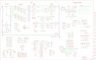
Card B-ALU & CU.png [ 366.92 KiB | Viewed 3460 times ]

As I mentioned, the ALU borrows heavily from Dieter Mueller's (ttlworks) Multiplexer ALU (http://6502.org/users/dieter/a1/a1_6.htm). I have come to admire this design a lot, and I especially like it because I found it just about when I was at a loss as to how to get a practical ALU built. Just like my TTL sequencer, a straight ahead gates based ALU would have been totally unwieldy and slow. This is one is very elegant, in my view. The overall structure is of a Logical Unit (LU) followed by an Adder and a Shifter.

In terms of how I've implemented here, the ALU has inputs A and B coming into it from the R Bus and the Data Bus respectively. B is latched on every cycle simply to split a memory read and a subsequent ALU operation over two cycles. The B input may alternatively by generated by the Sign Extension circuit, which saves the sign bit of a previous branch offset as it is loaded from memory to calculate the high-byte of a branch target address if a page-boundary is crossed.

The Logical Unit (LU) which is fed by the inputs and is comprised of 8 dual-multiplexers (74153s) which implement a lookup table for A and B - one multiplexer dedicated for each pair of bits in A and B. The function of the LU is driven by an LUOP consisting of four bits input to the data pins of the multiplexers. The net effect is that a given LUOP can cause a multiplexer to output a “1”, a “0”, the value of the A input, the value of the B input, Not A, Not B, A OR B, A AND B as well as A XOR B. Linking 8 multiplexers together therefore yields an 8 bit Logical Unit.

The LU is followed by a pair of adders which double up as a subtractor circuit when fed “A” and “NOT B” from the LU. The result of the adder then goes to a Shifter for right-shift operations (left-shift is accomplished by having the LU produce “A” on both inputs to the adder to add the value to itself). Each component can act as a pass-through under the control of various control lines to select the desired ALU operation (or combination thereof).

The BCD adjustment circuit taps the result of the adders and uses a 74151 multiplexer to detect values in excess of 0 - 9 which require adjustment. A pair of BCD adders then add 6 or 10 to perform the adjustment itself depending on whether we are adding or subtracting (10 being the two’s complement of 6). BCD Latch is used to latch an intermediate result and thereby spread the BCD operation over two cycles.

Rounding out the ALU are a number of flag “detection” and “selection” circuits to calculate the appropriate values for the “C”, “Z”, “V” and “N” flags. These take the result from the ALU (including from the B input directly in the case of a BIT operation) or in some cases a value directly from the Opcode (e.g., SEC, CLC - flag value is in bit 5 of the Opcode while bits 6 and 7 select which flag is affected). Finally, the P register takes the output of these flag circuits and latches them according to individual write-enable signals for each instruction.

As in the Registers Card, all the control logic is driven by a pair of ROMs which output signals into several decoders as follows:

A.MX is the simplest of these and is used only manage the A input of the ALU (“0”, A, B).

C.MX selects the Carry to use for various operations (IC being an Internal Carry used for address calculation) as well as controlling the Shifter and Sign-Extension circuits (LSR, ROR, ADS - Add Sign Ext, ADSIC - Add Sign-Ext using the Internal Carry).

The SF.MX decoder enables the write signals for the various flags in the P register, including writing to all of them during a PLP instruction. SF.MX can also directly implement setting the I flag (SEI) and clearing the D flag (CLD), although the latter is no longer used by the microcode. In addition, the OPCODE option tells the circuitry to set the appropriate flag based on the opcode itself (as described above). Finally, this decoder also enables the ALU itself (ALU.EN) and the BCD adjustment circuit (BCD.EN). When both these are disabled, data can bypass the ALU entirely, going directly from Data Bus to W Bus (ALU.BYPASS - used typically for register loads and transfers).

The NX.MX decoder drives the microcode sequencer and State Register (Q). As I’ve mentioned before, the State (Q) is used as the lower three bits of the address to the control ROMs to index into one of eight potential micro-instructions for every CPU instruction. Generally Q simply increments by 1 on each cycle and is set to 0 to begin the fetch-execute cycle. The microcode itself contains minimal logic facilities, with all functions handled in three NX.MX bits as follows:
Code:
0 - NEXT: Increment Q by 1
1 - END: Reset Q to zero on the next cycle. Ends the current instruction and will fetch a new opcode on the next cycle.
2 - END.C: for branches - set Q to 0 if no page boundary is crossed, otherwise increment Q by 1 to adjust ADH
3 - END.BTF: for branches - set Q to zero if the Branch Test Fails (branch not taken), otherwise increment Q by 1 to do the branch
4 - END1.DF: for decimal mode - set Q to 0 if the D flag is false, otherwise increment Q by 1 to perform a BCD operation
5 - END1: set Q = 1 to skip the fetch-opcode cycle for the next instruction when the opcode has been pre-fetched
6 - SKIP.ICC: skip the next micro-instruction if the Internal Carry is clear. Will skip unnecessary ADH calculations.

Most of the circuitry in NX.MX works to determine when the Q register should be set to 0 (the relevant signal is labeled /RESETQ in the schematic and is input to the /CLR pin of the Q 74161 counter). NX.MX decoder also derives the SKIP.TO.1 signal used for END1 and END1.DF, the SKIP.ICC signal, the BCD1 signal during the first cycle of a BCD operation and the INH.PF Inhibit Pre-Fetch signal to indicate if an interrupt is pending or one is active in cycles 0 and 1 of the interrupt sequence (INH.PF inhibits the incrementing of the Program Counter in those circumstances and will also inhibit a SKIP.TO.1 operation to ensure an interrupt is triggered in state Q=0).

The Interrupt Detection circuit to the right of and below the State Register (Q) is primarily concerned with setting the INT flag (Interrupt in progress), the /RST.INP flag (RESET In Progress) and the /NMI.INP flag (NMI In Progress). INT triggers the /IR.CLR signal to set the Instruction Register to zero (one of Dr. Jefyll’s suggestions) which in effect executes an implied BRK instruction. The /RST.INP and /NMI.INP flags then control the behaviour of the interrupt microcode sequence for each interrupt type (including selecting the correct interrupt vector address). These "In-Progress" flags are cleared by the /RESETQ signal which marks the end of every interrupt service sequence.

And that, I’m happy to say, is about it for the overall design. These two cards Registers and ALU & CU together comprise the bulk of the design. A lot of finicky boolean logic to get the decoders working right, but to be expected I think given the complexity of the instruction set. It’s true that the decoders could be radically simplified by extending the microcode to a wider control word, but this would contravene one of the specific design goals of the project - namely to keep the use of ROMs to a minimum. I know of a couple of optimizations I’ve yet to complete, and without a doubt there will be others yet to be discovered, but I dare say the design is starting to feel more complete at this stage. I have tested these circuits as best I can using Logisim and can say that by and large they are working - very pleased about that!

This continues to be an amazing learning experience - probably more like a crash course at this stage - and I’m loving picking up all the knowledge folks are so generously sharing. Many thanks to all once again. It feels great to get both these schematics posted and I’m looking forward to all the feedback.

My best to everyone,
Drass

_________________
C74-6502 Website: https://c74project.com


Top
 Profile  
Reply with quote  
 Post subject: Re: TTL 6502 Here I come
PostPosted: Fri Nov 27, 2015 7:45 pm 
Offline
User avatar

Joined: Fri Oct 30, 2015 9:49 pm
Posts: 54
Location: San Antonio, TX
Very interesting...

This is a great way of learning the inner workings on the CPU...


Top
 Profile  
Reply with quote  
 Post subject: Re: TTL 6502 Here I come
PostPosted: Fri Nov 27, 2015 10:19 pm 
Offline
User avatar

Joined: Sun Oct 18, 2015 11:02 pm
Posts: 428
Location: Toronto, ON
Alamorobotics wrote:
Very interesting...

This is a great way of learning the inner workings on the CPU...

Thanks Alamorobotics. Not sure I realized how deep the deep-end was when I jumped in ... just gotta keep swimming now. :) Getting ready for another weekend marathon.
Cheers!

_________________
C74-6502 Website: https://c74project.com


Top
 Profile  
Reply with quote  
 Post subject: Re: TTL 6502 Here I come
PostPosted: Mon Dec 28, 2015 5:02 pm 
Offline
User avatar

Joined: Sun Oct 18, 2015 11:02 pm
Posts: 428
Location: Toronto, ON
I thought I would do a brief update to let everyone know this project is still very much alive and well. It’s hard to believe it’s been a month since my last post. It won't come as a surprise to anyone that I severely under-estimated the effort involved in getting the original Logisim model onto a set of PCB boards ... quite a journey. Nevertheless, it's been great to work with and learn from ttlworks and Dr Jefyll. Their feedback has been invaluable and the overall effect is very clearly evident in a much cleaner design, more “authentic” 6502 behaviour, fewer ICs, and a substantial improvement in performance.

Attached are the latest schematics, which are nearing completion :wink:. Expectation is that this processor will run at 4MHz with HC logic and at 7MHz with AC logic - far beyond the original 1MHz target. All the current circuits have been verified in Logisim, which adds some degree of confidence that all this will work once laid out on a board - that part remains still a bit of magic I'm yet to get to. And lots of work remains before that in any case. Next up is to sort-out the interconnection between CPU boards and external bus structure and timing. I only have place-holders for signals up to this point so we'll see how that goes.

That’s all for now.

Best,
Drass


Attachments:
Card B-ALU & CU.png
Card B-ALU & CU.png [ 368.23 KiB | Viewed 3328 times ]
Card A-Registers.png
Card A-Registers.png [ 335.59 KiB | Viewed 3328 times ]

_________________
C74-6502 Website: https://c74project.com
Top
 Profile  
Reply with quote  
 Post subject: Re: TTL 6502 Here I come
PostPosted: Thu Feb 11, 2016 3:48 am 
Offline
User avatar

Joined: Sun Oct 18, 2015 11:02 pm
Posts: 428
Location: Toronto, ON
Hello folks,

Time flies (incredibly, it's been more than a month since my last post) ... but another milestone along the journey. With the schematics fairly stable now, attention has shifted to mechanical issues ... that is, for example, the fact that I want to fit this design on two Eurocard PCBs if at all possible. That pretty much has meant SMD parts, and so I've started a layout using SOIC packages. Having never managed anything more challenging than a simple pad-per-hole proto-board before, I am proceeding on faith here. As usual, deep-end first :)

I'm happy to report that the design is now fully cycle-exact with the NMOS 6502, including not requiring an extra cycle for decimal mode operations. When running in that mode, the processor generates only a valid C flag after an ADC or SBC instruction while the other flags are left undefined (and likely will be have a different value from what the NMOS 6502 will generate). I felt that was ok, since the NMOS 6502 does not claim to have "valid" results for these flags in any case. However, just for completeness, the processor will also have a jumper to set it into a two-cycle mode, where the BCD adjustment will take an extra cycle, and all flags will be set correctly as a result - like the 65C02 does. I thought this was a nice compromise between being authentic and practical.

Among other simplifications (and liberties taken) is one worth mentioning - the fact that /RES is treated like other interrupts in that the current instruction is allowed to finish before the RESET is recognized. Initially, I had made /RES take effect immediately, but in fact the whole thing could be simplified if writes to memory were disabled and the current instruction was allowed to complete. Candidly, I'm not sure how the NMOS 6502 handles this. The Rockwell 65C02 data sheet indicates that /RES being held low for two clock cycles will "cease microprocessing activity, followed by initialization after the positive edge of /RES". In my case, /RES being held low will simply disable writes to memory. The processor will initiate the reset sequence at the next SYNC cycle following the positive-edge of /RES. From what I can tell, allowing the processor to continue seems relatively harmless, but I'd be curious to know of any pitfalls. (I say relatively because merely reading certain addresses may in fact have a destructive effect on I/O devices, for example - but since a full RESET inevitably will follow, perhaps that's ok?).

So, that's it for now. Many thanks to ttlworks and Dr Jefyll for their many answers to my many questions. I would have never made it this far otherwise. It's on to layout and we'll have to see how that turns out ... in the meantime, Logisim has been running the Klaus test harness for about a week and a half now. I do hope it passes :)

Best regards,
Drass

_________________
C74-6502 Website: https://c74project.com


Top
 Profile  
Reply with quote  
 Post subject: Re: TTL 6502 Here I come
PostPosted: Fri Feb 12, 2016 11:19 pm 
Offline
User avatar

Joined: Sun Oct 18, 2015 11:02 pm
Posts: 428
Location: Toronto, ON
I just realized I never posted the schematics for the 6510 port. The objective here is to plug this processor into a C64 and of course that means it needs to be a 6510, rather than a 6502. The main difference being a 6 bit on-board I/O port. The port has a Data Direction Register (DDR) at address $0000 and the data port itself at address $0001.

The 6510 port in this case is built as an external peripheral - that is, it hangs off the processor's address and data buses just like any other external peripheral would but happens to reside "on-board" the CPU. This is an arbitrary distinction for a discrete design, but we do have to expose a different pinout for the 6510, so some special treatment was needed after all.

Attached is the schematic. You will see that in fact the circuit intercepts the 6502 bus lines and a separate header produces the 6510 pinout. If the port is not selected, a 74'245 allows signals to pass through untouched. Still not sure how exactly this will translate into a physical layout, but I hope the schematics are reasonably clear ... a couple of comparators to detect $0000 and $0001 and some individual buffers to implement the Data Direction Register functionality. Internally, it's an 8 bit port, with pull-downs resistors on bit 6 and 7. Bits 0-5 are exposed through the 6510 pinout. The port input lines are sampled on the rising-edge of PHI2 while writing to the DDR and port itself is on the falling-edge of PHI2. There are some series resistors on the headers, but that is still very much a work in progress.

So, that's it for now. With some luck, my next update will include some description of layout.

Best,
Drass


Attachments:
Card C-6510 Port.png
Card C-6510 Port.png [ 159.41 KiB | Viewed 3207 times ]

_________________
C74-6502 Website: https://c74project.com
Top
 Profile  
Reply with quote  
 Post subject: Layout - a start
PostPosted: Sun Feb 28, 2016 7:29 am 
Offline
User avatar

Joined: Sun Oct 18, 2015 11:02 pm
Posts: 428
Location: Toronto, ON
Hi Folks,

I'm super-excited to have finally started into the layout proper! As expected, I'm using SOIC parts and beginning with the registers card (Card A) ... and it's a dense one! Dieter (ttlworks) convinced me that the 6510 port and interface headers could be incorporated into this one board if components were placed on both sides of the card. It's definitely crowded, but so far think it will work. I thought I would share this as a work-in-progress to illustrate - lots of work yet to be done so please excuse any glitches at this stage. A few things might be worth pointing out:

  • There are two headers at the bottom, one for the 6510 pinout (flat pins pointing) and another for the 6520 pinout (vertical pins). All this was once on separate cards with two different adaptors and the 6510 port, but now it's all in here! Select the pinout you want and go! There is a solder jumper to enable the 6510 port. When disabled, the processor behaves like a 6502 with the correct pinout.
  • IDC ribbon connectors plug into the "pinout" headers and to an adaptor pcb which in turn plugs into a 6502 or 6510 socket on the motherboard. These are 80 pin connectors to allow for one ground connection per signal on the ribbon and there are series resistors on each connection to tame reflections.
  • There are a couple of DIP ICs in sockets as part of this interface. This is so "T" variant parts (e.g. HCT parts) can be used for TTL level input signals but replaced with regular parts otherwise. The larger IC can be even dispensed with altogether and jumpers installed instead in certain circumstances. The idea here is to support three different configurations: (a) when interfacing with a Commodore C64, for example, the "T" variant parts are used (e.g. HCT) and the 6510 port is enabled, (b) for a VIC20, "T" parts are used as well but the 6510 port is disabled, and (c) when interfacing with a CMOS based SBC, non "T" parts can be used and the larger IC optionally removed altogether and replaced with jumpers. This is probably a bit over the top, but decided to try to incorporate it all so the board could be "tuned" to each circumstance. It's all optional in any case, so no harm done in that respect.
  • On the lower left, there is a provision for powering the processor from a separate power supply if necessary (rather than from the host computer). There is solder jumper to select the power source.
  • Connectors on the top and left edges are inter-board connectors to Card B. So far it looks like I will be able to fir the entire design as a two Eurocard sandwich, which is great.

This a four layer board, with GND and VCC planes in internal layers, and so far I've managed to stay on the outer two layers but for a couple of short traces. I'm hoping to keep it that way and have solid planes to work with. Time will tell how dicey all this will get. Once I'm done placing vias (and I expect there will be lots of them), I'll want to arrange them so as to avoid chopping up the ground plane too badly ... but that's something for a later day.

Here is a pic of how things are looking so far:
Attachment:
Card A-Registers Brd.png
Card A-Registers Brd.png [ 45.4 KiB | Viewed 3134 times ]

And here is a pic showing the top layer removed to better show the components on the underside of the board.
Attachment:
Card A-Registers Brd bottom.png
Card A-Registers Brd bottom.png [ 33.14 KiB | Viewed 3134 times ]

That's it for now. The layout will keep me busy for quite some time yet, I expect.

My best to everyone,
Drass

_________________
C74-6502 Website: https://c74project.com


Top
 Profile  
Reply with quote  
 Post subject: Re: TTL 6502 Here I come
PostPosted: Fri Mar 04, 2016 4:37 am 
Offline
User avatar

Joined: Sun Oct 18, 2015 11:02 pm
Posts: 428
Location: Toronto, ON
Things are getting pretty crowded on the board ...
Attachment:
Card A-Registers Brd.png
Card A-Registers Brd.png [ 100.56 KiB | Viewed 3073 times ]
And I'm having to resort to traces on the VCC plane. Not the end of the world, but there is lots of routing yet to be done. Having components on both sides of the board makes for some very dense areas. Certainly, there are lots of vias already and many more likely will be needed. I'm trying to keep critical signals on single layers but not sure that will be possible in the end. We'll see ...

Cheers,
Drass

_________________
C74-6502 Website: https://c74project.com


Top
 Profile  
Reply with quote  
Display posts from previous:  Sort by  
Post new topic Reply to topic  [ 558 posts ]  Go to page Previous  1, 2, 3, 4, 5, 6, 7, 8 ... 38  Next

All times are UTC


Who is online

Users browsing this forum: dmsc, Google [Bot] and 14 guests


You cannot post new topics in this forum
You cannot reply to topics in this forum
You cannot edit your posts in this forum
You cannot delete your posts in this forum
You cannot post attachments in this forum

Search for:
Jump to: