6502.org Forum  Projects  Code  Documents  Tools  Forum
It is currently Tue Apr 23, 2024 9:23 pm

All times are UTC


Post new topic Reply to topic  [ 558 posts ]  Go to page Previous  1 ... 22, 23, 24, 25, 26, 27, 28 ... 38  Next
Author Message
 Post subject: Re: TTL 6502 Here I come
PostPosted: Sun Nov 19, 2017 10:38 pm 
Offline
User avatar

Joined: Sun Oct 18, 2015 11:02 pm
Posts: 428
Location: Toronto, ON
Ax2013 wrote:
Typically you set Address first, then CE and OE. Then ROMs work as planned (with MCU for example). In this setup, OE and CE are always enabled so it is not natural that addresses are changed on the fly. ... I was expecting spikes but not that strong.
Very interesting Axel. Thanks for sharing it. Makes me wish I had an oscilloscope so I could check this kind of thing for myself.

I could make a change in the next revision to output-enable those ROMs for only the second half of the cycle, once the address has settled. Not sure if it's necessary, but it certainly seems more tidy.

_________________
C74-6502 Website: https://c74project.com


Top
 Profile  
Reply with quote  
 Post subject: Re: TTL 6502 Here I come
PostPosted: Sun Nov 19, 2017 10:39 pm 
Offline
User avatar

Joined: Sun Oct 18, 2015 11:02 pm
Posts: 428
Location: Toronto, ON
Ax2013 wrote:
Hmmm doing some math here... Just wondering how many (xtal) clock phases are there in one opcode (eeprom microcode) phase? 20MHz has 2 x 25ns interval and EEPROM in the circuit diagram has 45ns access time.

Axel.
It's one clock-cycle per machine-cycle for this CPU, like on a 6502 MPU - that means one micro-instruction per cycle. However, the microcode is pre-fetched, and needed only at the end of the cycle. We therefore have the full 50ns to fetch the data - 45ns access time and 5ns for the 74AC163 to count up. Very tight but it should work!

_________________
C74-6502 Website: https://c74project.com


Top
 Profile  
Reply with quote  
 Post subject: Re: TTL 6502 Here I come
PostPosted: Mon Nov 20, 2017 2:31 am 
Offline
User avatar

Joined: Sun Oct 18, 2015 11:02 pm
Posts: 428
Location: Toronto, ON
I did further testing on the CPU over the weekend and managed to catch a few gremlins hidden in the brush. I now recall having to settle for very narrow tests in Logisim after the pipeline mods were made (regression tests had become prohibitively slow by then at an effective clock-rate of 100Hz). Even so, relatively few problems surfaced and I'm excited to share the results ...

Tests Performed:
  • Klaus Dormann's 6502 Test Suite using NMOS 6502 and 65C02 microcode - Passed
  • Klaus Dormann's 65C02 Test Suite using 65C02 microcode - Passed except for bugs noted below
  • Bruce Clark's NMOS Decimal Mode Test Suite - Passed
  • Drass' 'Unforseen' Opcodes Tests (UFOs) - Passed except for bugs noted below
  • IRQ pin - Blinky Light regular interrupt. Tests WAI opcode as well - Passed
  • /NMI, /SO, /VP, /ML, RDY pins - Passed

Tests yet to perform:
  • Bruce Clark's CMOS Decimal Mode Test Suite
  • 6510 Port Tests

Bug log:
  1. 65C02 Microcode - ADC (ind),Y: addressing broken.
    Fix --> 65C02 microcode/Opcode 71/line 2, change B := *DPt to B := *DP. Tested in Logisim. Passed.
  2. Card B - NOP1 (Single-Cycle NOP): CPU gets stuck if the following opcode is a single byte opcode.
    Caused by a FetchOpcode micro-instruction left in the MIR after the NOP1 is executed (we are actually expecting the normal FetchOperand second cycle). Can be fixed by triggering a switch to MIR2 (MIR.SW) after every FetchOpcode. (A FetchOperand Micro-instruction resides in MIR2 by default). This fix also bviates the special case to trigger a FetchOperand after a BranchExit.
    Fix --> Add /FETCHOP to 3-AND IC35 to force MIR.SW after every FetchOpcode, and Remove /BranchExit from Q.REG logic. Tested in Logisim. Passed.
  3. 65C02 Microcode - STP: Ignores following RESET.
    STP opcode requires a SYNC cycle to detect a reset. STP also exists in the 65816 microcode and as the KIL opcode in the NMOS 6502 microcode.
    Fix --> All Microcode/STP function/Line 2, change STP to "STP; IR := *PC; PC +=1". Tested in Logisim. Passed.
  4. Card B - Reset Detection: Missed button presses
    The CPU will ignore the reset if PHI1 goes high within 20ns of /RES going high.
    Fix --> insert a 74AC74 flip-flop clocked by PHI1 at the output of IC3A /RES NAND gate. Not yet tested.
  5. Power-on Sequence Fails
    Intermittent. Needs to be investigated.
  6. 6502 Microcode (UFO) - LXA: loads wrong byte into A and X
    Fix --> Micro-instruction "X := B" should enable the ALU: change from "30 02 C0" to "30 02 C8"
  7. 6502 UFOs - AXS, TAS, AHX:
    Needs investigation

And that's it so far! :D

Well, I'm thrilled, and that little CPU has performed like a champ! Most of these things are microde fixes, and the couple of hardware patches needed are quite manageable. I still have to run a few more functional tests, but it's really coming along ... very exciting to be making this progress. :mrgreen:

Cheers for now,
Drass

_________________
C74-6502 Website: https://c74project.com


Top
 Profile  
Reply with quote  
 Post subject: Re: TTL 6502 Here I come
PostPosted: Mon Nov 20, 2017 5:25 am 
Offline

Joined: Thu Jul 27, 2017 7:48 pm
Posts: 68
Drass wrote:
45ns access time and 5ns for the 74AC163 to count up. Very tight but it should work!


Very tight indeed! Very interested to see how it works in practice.
For me, the scope is almost mandatory for such applications. I even considered building a simple logic analyzer when starting TTL CPU but didn't need that after all.

Axel.


Last edited by Ax2013 on Mon Nov 20, 2017 7:22 pm, edited 1 time in total.

Top
 Profile  
Reply with quote  
 Post subject: Re: TTL 6502 Here I come
PostPosted: Mon Nov 20, 2017 9:00 am 
Offline

Joined: Thu Jul 27, 2017 7:48 pm
Posts: 68
Drass wrote:
I could make a change in the next revision to output-enable those ROMs for only the second half of the cycle, once the address has settled. Not sure if it's necessary, but it certainly seems more tidy.


I don't think it is necessary. There might be some behavior during address is setting.. or not. Is it affecting your application... we'll see. Without a scope, this is an academical discussion anyway. And I was specifically curious what happens in practice.
Putting output to the 3rd mode leaves input pins floating. This might have side effects.

Axel.


Top
 Profile  
Reply with quote  
 Post subject: Re: TTL 6502 Here I come
PostPosted: Thu Nov 23, 2017 6:58 am 
Offline
User avatar

Joined: Fri Nov 09, 2012 5:54 pm
Posts: 1392
Drass wrote:
5. Power-on Sequence Fails

IMHO the source of this problem most likely could be the MIR.SW flipflop IC32 (74LVC1G74 D_flipflop) on the ALU&CU PCB.

From the schematics, isn't tied to /RES.
So we don't know for sure if it's cleared or set at power_on.
If its in the wrong state at power_on, there is a chance that it somehow disrupts the RESET microcode sequence.

Please check.


Top
 Profile  
Reply with quote  
 Post subject: Re: TTL 6502 Here I come
PostPosted: Fri Nov 24, 2017 3:47 pm 
Offline
User avatar

Joined: Sun Oct 18, 2015 11:02 pm
Posts: 428
Location: Toronto, ON
Thanks for the pointer. I’ll take a closer look at that (maybe this weekend).

The idea here was that the various control flip-flops inside the CPU (including MIR.SW) would get a chance to assume a valid state while /RES is held low on startup. The SBC has a Maxim DS1813 which holds /RES low for 150ms on power-up. The CPU disables memory writes but otherwise runs “normally” during that time, so that should set all the internal registers to a consistent state. At least that’s the theory - obviously something has gone awry. Curious to see what happened. :)

_________________
C74-6502 Website: https://c74project.com


Top
 Profile  
Reply with quote  
 Post subject: Re: TTL 6502 Here I come
PostPosted: Sat Nov 25, 2017 3:39 pm 
Offline
User avatar

Joined: Sun Oct 18, 2015 11:02 pm
Posts: 428
Location: Toronto, ON
And now, time for a little fun: introducing the C74 Socket Adapter! ;)
  • A convenient way to connect the TTL CPU to any 6502-based computer
  • Configurable VDD and GND pins to support NMOS 6502, 6510 and CMOS 65C02 pinouts
  • Dual 40-pin headers provide ample grounding for high-frequency applications
  • Designed especially for the C74 project with guidance from dr Jefyll

Here is the little critter:
Attachment:
C74-Socket 1.jpg
C74-Socket 1.jpg [ 63.04 KiB | Viewed 1448 times ]

Sure makes the TTL CPU look like a proper insert-replacement on the SBC! :)
Attachment:
C74-Socket 2.jpg
C74-Socket 2.jpg [ 125.89 KiB | Viewed 1448 times ]

I also took the time finally to heed dr Jefyll advice and connect the CPU boards together in overlapped fashion. The inter-card connections along the middle of the assembly are now as short as possible but still allow access the boards for debugging. Below is a better look at the arrangement:
Attachment:
C74-Socket 3.jpg
C74-Socket 3.jpg [ 110.11 KiB | Viewed 1448 times ]

It turns out that making these changes, and replacing a flaky reset button, seem to have fixed the intermittent power-up and reset problems I was having. Ah, yes, construction issues bite again! (thank you Jeff!) :)

Ok, now on to the other bugs ... 8)

_________________
C74-6502 Website: https://c74project.com


Top
 Profile  
Reply with quote  
 Post subject: Re: TTL 6502 Here I come
PostPosted: Sun Nov 26, 2017 9:39 am 
Offline
User avatar

Joined: Thu Dec 11, 2008 1:28 pm
Posts: 10793
Location: England
Very nice - thanks for the photos!


Top
 Profile  
Reply with quote  
 Post subject: Re: TTL 6502 Here I come
PostPosted: Mon Nov 27, 2017 2:31 am 
Offline
User avatar

Joined: Sun Oct 18, 2015 11:02 pm
Posts: 428
Location: Toronto, ON
Well, I couldn't be happier with the state of affairs. Here's the Sunday night report:

Fix Log

  • 65C02 NOP1 (Single-Cycle NOP): PCB Logic - fixed, verified.
  • 6502 UFOs AXS, TAS, AHX: Poor solder joints - fixed, verified.
  • Reset issues: Poor construction - fixed, verified.
  • 65C02 ADC (ind),Y: Microcode - fixed, verified.
  • 65C02 STP: Microcode - fixed, verified.
  • 6502 UFO LXA: Microcode - fixed, verified.
  • STA (ind),Y always takes 6 cycles: Microcode - fixed, verified.

Having put the CPU through its paces and fixed the known bugs, I can safely say I'm astonished. Only one hardware logic error came up -- 'C02 single-cycle NOPs. The fix required lifting a pin on one of those tiny SOT23 packages and patching around it, but was otherwise straight forward. Beyond that, the problems stemmed from simple transcription errors or poor construction and grounding. Some good lessons there, but all in all, I'm very pleased indeed.

A significant caveat to this being a faithful recreation did surface in the form of CMOS Decimal Mode SBC operations -- it turns out that invalid BCD input values produce different results on the NMOS 6502 vs. the 65C02. Bruce Clark describes these differences briefly here, but I have to confess to not fully grasping the effects until the test suite revealed them (for example, "0 - 11" generates 89 on both processors, but "0 - $b" generates $9F on the 6502 and $8F on the 65C02). It's probably a minor trangression in the scheme of things, but it was enough to cause the CPU to fail the CMOS variant of Bruce Clark's Decimal Mode test suite.

Nevertheless, I'm calling it: the functional tests are now complete and the CPU gets a passing grade! (Yes, indeed, what we have here, folks, is a genuine, bonafide TTL 6502! And it's a beauty! :D ... So good! ... so good.)

Next up is the 6510 port, serial I/O and running Basic on the SBC; and of course speed tests. Fingers remain firmly crossed on the 20MHz question, but I can offer this harbinger now: the IRQ-Blinky Light test ran reliably at 12MHz :shock: -- getting closer ... 8)

I'd like to build V2 of the SBC before going too much further. It's important now to remove any potential problems with flaky wait-states or unqualified reads on the SBC. I can also verify in passing whether the spurious read during indexed-absolute addressing persists once things are cleaned up.

Cheers for now,
Drass

_________________
C74-6502 Website: https://c74project.com


Top
 Profile  
Reply with quote  
 Post subject: Re: TTL 6502 Here I come
PostPosted: Mon Nov 27, 2017 1:20 pm 
Offline
User avatar

Joined: Fri Nov 09, 2012 5:54 pm
Posts: 1392
Congratulations: 12MHz, and the bug list went fixed.


IMHO the CPU would be mainly running NMOS 6502 machine code later.

So I think that little difference between NMOS 6502 and 65C02 when it comes to decimal SBC with invalid BCD input numbers
isn't too critical. (Just mention this little difference in the CPU datasheet later.)

Designing a fast NMOS 6502 BCD correction circuitry took us some weeks, and I'm afraid that trying to modify it for having
a 100% 65C02 BCD compatible mode of operation would take us some more weeks... while generating some _other_ bugs.

It would be wise to leave the BCD correction in the CPU as it is, and to make designing 65C02 compatible BCD arithmetic circuitry
a "homework assignment for the experienced reader".


Let's hope, that the BASIC interpreter will be working as intended on the CPU.
Hardware debugging sure is more fun when having RS232 and a monitor program.
Looking forward to see, how the K24 PCB turns out.
Go, Drass, go. :)


Top
 Profile  
Reply with quote  
 Post subject: Re: TTL 6502 Here I come
PostPosted: Mon Nov 27, 2017 9:30 pm 
Offline
User avatar

Joined: Sun Oct 18, 2015 11:02 pm
Posts: 428
Location: Toronto, ON
ttlworks wrote:
I'm afraid that trying to modify it for having a 100% 65C02 BCD compatible mode of operation would take us some more weeks... while generating some _other_ bugs.
Not to mention the fact that the NMOS BCD logic path takes 46ns already and there is precious little PCB real estate left-- no room to maneuver in either direction! :(

_________________
C74-6502 Website: https://c74project.com


Top
 Profile  
Reply with quote  
 Post subject: Re: TTL 6502 Here I come
PostPosted: Mon Dec 04, 2017 3:59 am 
Offline
User avatar

Joined: Sun Oct 18, 2015 11:02 pm
Posts: 428
Location: Toronto, ON
During last week's tests, the CPU ran reliably at 12MHz, but failed at 16MHz. Given that jumpers are still very much in use between the PCBs, it's easy to assume poor grounding is the culprit at the higher speed, or perhaps that 12MHz might be the ceiling on performance. I wanted to find out. But first I needed to deal with the fact that 16MHz was going to be impossible while running the code from ROM (at least until V2 of the SBC is built).

Easy enough. The CPU can copy the "blinky-light" loop to RAM using the SBC's half-speed SLOW clock before jumping to it. Then the 16MHz FAST clock can be manually engaged to run the remainder of test from RAM. I calculated bit 0 of the VIA Port would flicker at roughly 890KHz if things were working correctly (the blinky loop is just 9 cycles, so 18 cycles for a full "blink", at 16MHz / 18 = 888.88KHz blink-rate). But alas, the CPU only sputtered and locked-up when I ran the test -- no blinking at all. Ok, so something else was gumming up the works.

I then remembered that there are two gates in series on the CPU's internal clock pin, one implements RDY and the other the 2-cycle-BCD internal wait-state. That's all well and good, but two gates translates into a 10ns delay after the fall of PHI2 before the CPU can start to work! Including these two gates, the minimum half-cycle is a full 33ns, or a top speed of only 15MHz -- there's no way this was going to work under those circumstances!

Thankfully, the CPU includes a Zero Delay Buffer ("ZDB" - datasheet attached below) to deal with exactly this problem. The idea here, I learned from dr Jefyll, is to synchronize the internal clock after the gates with the input clock before the gates, such that the edges of the two signals are co-incident. The ZDB does just that by way of an additional brief delay it calculates automatically. Of course the downstream logic can't tell one cycle from the next, so the gate delays are eliminated altogether and the CPU responds 10ns more quickly than it otherwise would! (I know, magic right?). Here is the circuit in question:
Attachment:
Card A-Registers Sch p3.png
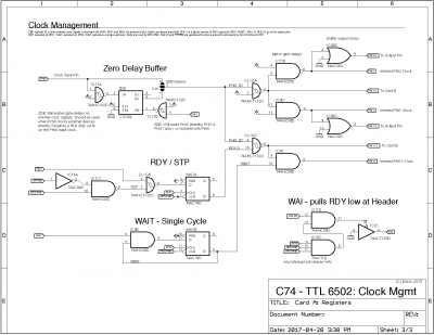
Card A-Registers Sch p3.png [ 23.03 KiB | Viewed 1193 times ]

Now the ZDB requires that the input clock-rate be no lower than 5MHz, so single-stepping the CPU for debugging is impossible when the ZDB is engaged. I had therefore placed it behind a solder-jumnper so it could be safely disabled until needed. And clearly, it was now very much needed! So, I soldered the jumper closed and hooked up my cheapy-ebay frequency counter to read bit 0 of the VIA port. I paused for a moment to look at the frequency readout before flipping to the FAST clock, and then:
Attachment:
Freq 888.jpg
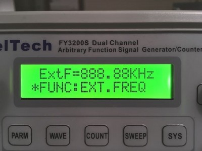
Freq 888.jpg [ 38.51 KiB | Viewed 1193 times ]
Bang on, unbelievable! :shock:

The fan on the power-supply was churning away and the display showed 600mA at 5V. Man, oh man, that TTL CPU was hammering the VIA port at 16MHz!!! Amazing ... :)

On other news, I was able to confirm that the 6510 port works, as does the 6502+NOPs alternate microcode. It seems further patches to the PCBs might be less likely at this stage of testing (I hope), so it's finally come time to stack the CPU boards together. Unfortunately, the inter-card connectors I used don't actually fit together. :roll: The new ones I ordered have arrived, so it's likely I will spend next weekend wrestling with the boards to replace the connectors.

Cheers for now,
Drass

EDIT: removed the mention that the ZDB requires a 50% duty-cycle. I must have been confused about the requirement.


Attachments:
CY2302_ZDB.pdf [1.16 MiB]
Downloaded 74 times

_________________
C74-6502 Website: https://c74project.com


Last edited by Drass on Tue Dec 05, 2017 3:39 am, edited 1 time in total.
Top
 Profile  
Reply with quote  
 Post subject: Re: TTL 6502 Here I come
PostPosted: Mon Dec 04, 2017 5:14 am 
Offline

Joined: Thu Jul 27, 2017 7:48 pm
Posts: 68
:-)


Top
 Profile  
Reply with quote  
 Post subject: Re: TTL 6502 Here I come
PostPosted: Mon Dec 04, 2017 9:24 am 
Offline
User avatar

Joined: Fri Nov 09, 2012 5:54 pm
Posts: 1392
After doing some math, it looks like the difference between NMOS 6502 and 65C02 decimal SBC is:

In the 65C02, if the carry output of the Bit 3..0 ALU adder is 0, causing a BCD correction for Bit 3..0,
and the carry output of the Bit 3..0 correction adder (adding $A) is 0 too, Bit 7..4 have to be decremented.

;---

For the TTL CPU, this means that we would have to modify the constant generator for the Bit 7..4 BCD correction adder.
Instead of generating just $0, +$6, -6 (= +$0A), we now would need: $0, +$6, -1 (= +$F), -6 (= +$0A), -7 (= +$09).

Since BCD arithmetic takes two cycles on the 65C02, adding a little delay to the 65C02 specific signal paths won't be much of a problem,
we just need to take care not to add any delays to the NMOS specific signal paths because they seem the be critical for maximum CPU speed.

IMHO modifying the BCD circuitry would require to have 2*74CBT3253 for BCD.SEL.HI, plus a three input NOR gate, plus an inverter.
IIRC there is a spare inverter plus some spare OR gates on the ALU&CU PCB, the three input NOR maybe could be "substituted" by two OR gates.
But I'm not sure if there is enough free space on that PCB for adding another chip, and modifying the PCB layout certainly won't be fun.

Some crude C code attached for proving my concept. (I'm not much of a coder.)
I only have checked for the results of decimal SBC, not for the flag evaluation of decimal BCD.
ADC completely untested, take care.


Attachments:
BCD_TEST.C [4.2 KiB]
Downloaded 59 times
Top
 Profile  
Reply with quote  
Display posts from previous:  Sort by  
Post new topic Reply to topic  [ 558 posts ]  Go to page Previous  1 ... 22, 23, 24, 25, 26, 27, 28 ... 38  Next

All times are UTC


Who is online

Users browsing this forum: No registered users and 10 guests


You cannot post new topics in this forum
You cannot reply to topics in this forum
You cannot edit your posts in this forum
You cannot delete your posts in this forum
You cannot post attachments in this forum

Search for:
Jump to: