6502.org Forum  Projects  Code  Documents  Tools  Forum
It is currently Fri Apr 26, 2024 6:54 am

All times are UTC


Post new topic Reply to topic  [ 10 posts ] 
Author Message
 Post subject: ROMulus the 1st
PostPosted: Tue Sep 15, 2015 7:40 am 
Offline
User avatar

Joined: Sun Oct 13, 2013 2:58 pm
Posts: 485
Location: Switzerland
After a series of tests and proof of concepts I finally put all the pieces together and built the first version with all features together on a breadboard. "ROMulus the 1st", named after the fact that it is my first fully functional ROM less SBC.

Attachment:
File comment: Overview of the breadboard
IMG_0348.JPG
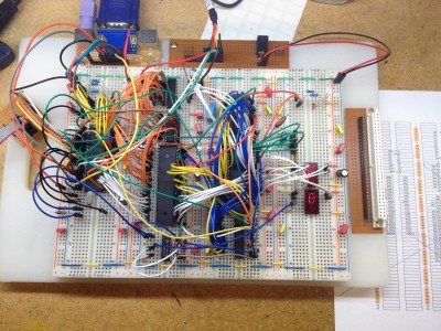
IMG_0348.JPG [ 3.26 MiB | Viewed 1983 times ]


It has the following features

    W65C816 processor, not because it is needed but because it's the only CMOS version I currently have, a CMOS version is mandatory
    AS7C1024-20PC 128kbyte SRAM although only 64kbyte are used
    VGA text display (supporting 24x40 and 24x80 characters) using a 4k Dual-Port RAM (IDT7134)
    PS/2 keyboard
    The ROM Image is loaded to the RAM using the IML/blink-load method

The VGA signal is generated using a ATMega1284P. The MCU uses a 22.1184MHz baud-rate crystal. This is also the VGA pixel clock. The VGA timing uses the 640*480@60Hz standard, but with only 560 pixels. A 74HC166 is used as the parallel to serial shift register to create the pixels and a 74HC573 is used as I/O port expansion.

Attachment:
File comment: VGA Display
IMG_0355.JPG
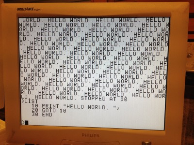
IMG_0355.JPG [ 3.63 MiB | Viewed 1983 times ]


The 22.1184MHz was selected to

    support higher baud-rates (115200baud) for the XModem upload function
    support 7-bit wide character ROMs of legacy systems that have patterns which look good only with 7-bits per character
    only slightly overclock the MCU

The same MCU also implements the PS/2 keyboard interface. For this the second USART is used in synchronous mode in order to avoid polling or interrupts that could disturb the VGA signal generation. Also the same MCU is used to implement the IML/blind-load feature to initialise the RAM with the ROM Image. For this a 74HC574 has been added that together with the GAL22V10 build the byte buffer that acts as "bootstrap-ROM" during initialisation.

The ATMega1284P has a huge flash (128kbyte) which has room for many more. Currently it contains the code, the CGROM(s) and a 12kbyte 6502 ROM Image which together only occupy 20% of the flash.

The glue logic uses a GAL22V10 and a 74AC00. The GAL implements the key wait flag and the address decoder. The 74AC00 is responsible for the Master-Read and the Master-Write signal (read and write enable signals qualified with PHI2). At the moment the memory map uses the old Apple II scheme and looks like the following

    $0000..$BFFF RAM
    $C000..$C00F Keyboard Buffer holding the ASCII code in Bits 0..6 and the key wait flag in D7
    $C010..$C01F Clear the key wait flag
    $C020..$C0FF General IO
    $C100..$CFFF RAM for IO support routines, write protected after initialisation
    $D000..$FFFF RAM for the ROM Image, write protected after initialisation

I used the Apple II scheme so I could be using the original Apple II ROM (D0,E0, E8, F0, F8 ROMs) giving me time to concentrate on the MCU code first until everything worked. As all the address decoding takes place in the GAL22V10 the memory map can be easily adopted to the final needs without changing the wiring.

The same MCU is also generating the PHI2 clock. During the initialisation it "manually" controls the state of PHI2 to load the ROM image. PHI2 is using OC2B of Timer 2 and once the image is loaded I connect the PIN to the Timer to create the system clock. The maximum system clock that can be created in this way is half the MCU clock rate. I currently run the system at the maximum of 11MHz and it's stable.

The MCU also provides a user interface via RS-232 that allows to perform the most basic system controls.

    Reset the 65xx system
    Start and Stop PHI2, PHI2 can be set to 11/(N+1)MHz, where N=0..127
    Show the system status (VPB, RES, IML, PHI2 when in manual mode)
    Download a 6502 image via XModem to the RAM
    Load a ROM image in the MCU flash to the RAM
    Control IML (Initialisation Mode)
    Ouput a value to the keyboard buffer
    Single cycle PHI2

You can set an initial command so you do not need a terminal to start up the system.

Next will be the clean-up. First I will create some decent documentation. Then the MCU code needs an urgent restructuring and house-keeping. When this is done I'll start with ROMulus the 2nd that will have on-board ACIA, VIA and compact flash interface. Also it will use a CPLD instead of the GAL so everything can be defined in software and downloaded to the board.

Cheers

Peter


Top
 Profile  
Reply with quote  
 Post subject: Re: ROMulus the 1st
PostPosted: Tue Sep 15, 2015 7:44 am 
Offline
User avatar

Joined: Thu Dec 11, 2008 1:28 pm
Posts: 10793
Location: England
Great work! Does the MCU only need to provide a single byte of data during load, counting cycles and performing a series of (for example) LDA immediate; STA absolute instructions? Or does it control the address bus?


Top
 Profile  
Reply with quote  
 Post subject: Re: ROMulus the 1st
PostPosted: Tue Sep 15, 2015 7:58 am 
Offline
User avatar

Joined: Sun Oct 13, 2013 2:58 pm
Posts: 485
Location: Switzerland
Thanks. The MCU only feeds bytes and during this time controls PHI2. It blindly counts cycles. After reset it creates cycles until the 65C816 requests the reset vector address then it starts to feed the bytes of the following instructions

Code:
      *=$300
LOOP   LDA   #data
      STA   address
      JMP   LOOP


it actually starts with the address section of the JMP instruction which is used as reset vector as well. The only signal the MCU needs to provide are the boot status signal for the memory decoder (I called it IML), PHI2, RES. For Bits D0..6 I use a 74ACT574 as the byte buffer which is loaded by the MCU with the byte and read by the 6502, bit D7 is implemented in the GAL as it serves two function, first it acts as D7 of the byte buffer (IML=High) and later it acts as the key wait flag for the ASCII PS/2 keyboard interface. To save pins on the MCU you could as well use a 74HCT595 intead the 74HCT574, speed is not an issue during initialisation.


Last edited by cbscpe on Tue Sep 15, 2015 10:11 am, edited 1 time in total.

Top
 Profile  
Reply with quote  
 Post subject: Re: ROMulus the 1st
PostPosted: Tue Sep 15, 2015 8:26 am 
Offline
User avatar

Joined: Thu Dec 11, 2008 1:28 pm
Posts: 10793
Location: England
Thanks!


Top
 Profile  
Reply with quote  
 Post subject: Re: ROMulus the 1st
PostPosted: Wed Sep 16, 2015 6:19 pm 
Offline
User avatar

Joined: Sun Oct 13, 2013 2:58 pm
Posts: 485
Location: Switzerland
So here is the first set of documents I have created. First the schematic in two sheets

Attachment:
File comment: Schematic 1st Page
Romulus1st-1-2.png
Romulus1st-1-2.png [ 50.86 KiB | Viewed 1927 times ]


Attachment:
File comment: Schematic 2nd Page
Romulus1st-2-2.png
Romulus1st-2-2.png [ 35.13 KiB | Viewed 1927 times ]


And the WinCUPL design file of the GAL

Code:
Name     romlessv1 ;
PartNo   00 ;
Date     06.09.2015 ;
Revision 01 ;
Designer cbscpe ;
Company  privat ;
Assembly None ;
Location CH ;
Device   g22v10 ;

/* *************** INPUT PINS *********************/
PIN    1 =  KEY                    ; /*  Set key wait clock             */
PIN    2 =  A15                    ; /*                                 */
PIN    3 =  A14                    ; /*                                 */
PIN    4 =  A13                    ; /*                                 */
PIN    5 =  A12                    ; /*                                 */
PIN    6 =  A11                    ; /*                                 */
PIN    7 =  A10                    ; /*                                 */
PIN    8 =  A9                     ; /*                                 */
PIN    9 =  A8                     ; /*                                 */
PIN   10 =  A7                     ; /*                                 */
PIN   11 =  A6                     ; /*                                 */
PIN   13 =  RW                     ; /*                                 */
PIN   14 =  PHI2                   ; /*                                 */

/* *************** OUTPUT PINS *********************/
PIN   15 = !IOA                    ; /*  $C08x, 2x, Bx, 4x, Dx-Fx       */
PIN   16 = !EXT                    ; /*  External Range, e.g. Video RAM */
PIN   17 = !IOB                    ; /*  Select for 65xx peripherals    */
PIN   18 = !RAM                    ; /*                                 */
PIN   19 = !BYTE                   ; /*  Boot / Key Buffer              */
PIN   20 =  KW                     ; /*  Key Wait Flag                  */
PIN   21 =  IML                    ; /*  boot mode Initial Machine Load */
PIN   22 =  A4                     ; /*                                 */
PIN   23 =  A5                     ; /*                                 */

FIELD   ADDRESS = [A15..0];

KW.ar  =  ADDRESS:[C010..C01F] &  PHI2;

KW.d   = !IML
   #  IML & PHI2;

KW.sp   = 'h'00;

KW.oe   =  BYTE;

EXT   =  ADDRESS:[0400..0BFF] & !IML
   #  ADDRESS:[0000..0FFF] &  IML  & !RW;

IOA   =  ADDRESS:[C080..C08F] & !IML
   #  ADDRESS:[C020..C02F] & !IML
   #  ADDRESS:[C0B0..C0BF] & !IML
   #  ADDRESS:[C040..C04F] & !IML
   #  ADDRESS:[C0D0..C0FF] & !IML;

IOB   =  ADDRESS:[C090..C09F] & !IML
   #  ADDRESS:[C0A0..C0AF] & !IML
   #  ADDRESS:[C0C0..C0CF] & !IML
   #  ADDRESS:[C080..C0FF] &  IML  & !RW;

BYTE   =                          IML  &  RW  &  PHI2
   #  ADDRESS:[C000..C01F] & !IML  &  RW  &  PHI2;

RAM   =                          IML  & !RW
   #  ADDRESS:[0000..03FF] & !IML
   #  ADDRESS:[0C00..BFFF] & !IML
   #  ADDRESS:[C100..FFFF] & !IML  &  RW;


Cheers

Peter


Top
 Profile  
Reply with quote  
 Post subject: Re: ROMulus the 1st
PostPosted: Wed Sep 16, 2015 8:20 pm 
Offline
User avatar

Joined: Wed Feb 13, 2013 1:38 pm
Posts: 586
Location: Michigan, USA
Nice work, Peter... Looks great...


Top
 Profile  
Reply with quote  
 Post subject: Re: ROMulus the 1st
PostPosted: Sun Sep 27, 2015 2:49 pm 
Offline
User avatar

Joined: Mon May 25, 2015 2:25 pm
Posts: 632
Location: Gillies, Ontario, Canada
Always great to see a tangle of wires generating crisp video!
Kudos on your project, and I like the name.

Brad


Top
 Profile  
Reply with quote  
 Post subject: Re: ROMulus the 1st
PostPosted: Sun Sep 27, 2015 3:37 pm 
Offline
User avatar

Joined: Fri Aug 30, 2002 9:02 pm
Posts: 1681
Location: Sacramento, CA
Great job Peter!

One question about the schematics, on sheet 1, is the parallel input to the shift register supposed to be VA0..6,11? I was expecting to find VD0..7.

I'll look forward to watching your progress!!

Daryl

_________________
Please visit my website -> https://sbc.rictor.org/


Top
 Profile  
Reply with quote  
 Post subject: Re: ROMulus the 1st
PostPosted: Sun Sep 27, 2015 7:47 pm 
Offline
User avatar

Joined: Sun Oct 13, 2013 2:58 pm
Posts: 485
Location: Switzerland
Michael wrote:
Nice work, Peter... Looks great...


Thanks

Oneironaut wrote:
Always great to see a tangle of wires generating crisp video!
Kudos on your project, and I like the name.


Yeah I'm really proud of my VGA solution, I even have version with low and high res graphic, not as much pixels and colours as yours but I have a very low chip count.

8BIT wrote:
Great job Peter!

One question about the schematics, on sheet 1, is the parallel input to the shift register supposed to be VA0..6,11? I was expecting to find VD0..7.


That's correct. This is on purpose. One issue I have is that the 80-column display only leaves 7 cycles per character and that I only can update 8-bits of the video RAM address. So I need to pack all address bits that might change in a row into the lower 8 address bits. The mapping you see is used when the VGA controller is used in my Apple IIe clone. The Apple II normally packs 3 character rows with 40 characters each into one linearly addressable memory block of 128bytes (3 x 40 leaving 8 bits per block unused). Thats why I have VA0..6 in the low-byte and I only need to change VA0..6 when I build the video display. VA11 is then added to the lower address byte so I can toggle the highest address bits for every other character when I mimic the Apple IIe 80-column mode and still only need to change one byte of address bits. The 6502 in Apple IIe mode then connects A0..A10 to address lines A0R to A10R of the DPRAM and A11R of the DPRAM would then connect to the Main/Aux RAM selector signal.


Cheers

Peter


Top
 Profile  
Reply with quote  
 Post subject: Re: ROMulus the 1st
PostPosted: Mon Sep 28, 2015 12:32 pm 
Offline
User avatar

Joined: Sun Oct 13, 2013 2:58 pm
Posts: 485
Location: Switzerland
Hi,

cleanup of code has made some progress so that I can now upload a version for your entertainment before I go on vacations for some weeks. I'll have internet but no development environment, so there will be no progress during my holidays :lol:
Attachment:
File comment: Archive of AVR Studio Project Folder
ROMulus1st.zip [74.36 KiB]
Downloaded 102 times

As usual all my stuff uses assembler. Have fun!

Cheers

Peter


Top
 Profile  
Reply with quote  
Display posts from previous:  Sort by  
Post new topic Reply to topic  [ 10 posts ] 

All times are UTC


Who is online

Users browsing this forum: No registered users and 28 guests


You cannot post new topics in this forum
You cannot reply to topics in this forum
You cannot edit your posts in this forum
You cannot delete your posts in this forum
You cannot post attachments in this forum

Search for:
Jump to: