6502.org Forum  Projects  Code  Documents  Tools  Forum
It is currently Wed Apr 24, 2024 4:23 am

All times are UTC


Post new topic Reply to topic  [ 25 posts ]  Go to page Previous  1, 2
Author Message
PostPosted: Fri Aug 21, 2015 3:53 pm 
Offline
User avatar

Joined: Thu May 28, 2009 9:46 pm
Posts: 8140
Location: Midwestern USA
cbscpe wrote:
I'm still not convinced, because this
BigDumbDinosaur wrote:
Tor wrote:
My guess is that when BDD said "verboten" it is in relation to setting up a protected execution environment (as BDD wrote later in the paragraph).

Correct. Whatever term is used to describe these instructions, they would either be instructions that should never be executed (STP immediately comes to mind) or should not be executed when the system is operating in user mode.

will result in a highly complex system. In my opinion the out of the box 6502/816 is not suited for a protected OS. In addition this would not only require inhibiting privileged instructions but also some sort of memory protection scheme, which, especially for the stack, will be very tricky. Without a dedicated supervisor mode stack pointer it is in my opinion near to impossible. If you are interested in building a protected OS you should rather look at other "legacy" architectures which are as well fun to play around with. For this I have my DCJ11A based SBC.

The development of a protected operating environment with the 65C816 is something discussed in detail in my POC V2 series of posts, starting here.

_________________
x86?  We ain't got no x86.  We don't NEED no stinking x86!


Top
 Profile  
Reply with quote  
PostPosted: Fri Aug 21, 2015 4:51 pm 
Offline
User avatar

Joined: Sun Oct 13, 2013 2:58 pm
Posts: 485
Location: Switzerland
I know and I have already read through most of it. It was very interesting, but you certainly must agree this will be a rather complex system.


Top
 Profile  
Reply with quote  
PostPosted: Sat Aug 22, 2015 1:36 am 
Offline
User avatar

Joined: Thu May 28, 2009 9:46 pm
Posts: 8140
Location: Midwestern USA
cbscpe wrote:
I know and I have already read through most of it. It was very interesting, but you certainly must agree this will be a rather complex system.

Yes, it will be complicated. However, where's the challenge in the simple stuff? :lol:

POC V2 will not have enough hardware resources to do what I envision but I think there will have enough to at least try out the kernel/user mode and bank $00 remapping concepts. If I can make that part of it fly then a major hurdle has been leaped in getting a protected environment up and running. POC V3 will have a much larger CPLD, as well as much more RAM, so it might have what is needed to do the job.

Speaking of POC V2, I reworked its PCB layout to accommodate a JTAG port—I'll be posting my changes in the next day or two. Having a JTAG port should allow me to program the CPLD without having to wait on Atmel for the needed adapter, since the adapter's ship date has been pushed back yet again. :twisted:

_________________
x86?  We ain't got no x86.  We don't NEED no stinking x86!


Top
 Profile  
Reply with quote  
PostPosted: Sat Aug 22, 2015 7:54 am 
Offline
User avatar

Joined: Thu Dec 11, 2008 1:28 pm
Posts: 10793
Location: England
OK, so one of you is interested in simple systems and the other in the opposite. The aim of the thread is to collect a correct and understandable summary of the 816's pins. (I doubt that the summary can also be simple.)


Top
 Profile  
Reply with quote  
PostPosted: Sat Aug 22, 2015 1:36 pm 
Offline

Joined: Mon Jan 07, 2013 2:42 pm
Posts: 576
Location: Just outside Berlin, Germany
Dr Jefyll wrote:
I know you're being somewhat humorous here, Scot, just as you were when you mentioned "trickery" in regard to the VPB output.


Yes, that was flippery on my part. Life would be a lot easier without those two pins ... but I do recognize that they bring Good Things (TM) to the table in some circumstances.


Top
 Profile  
Reply with quote  
PostPosted: Sat Aug 22, 2015 7:38 pm 
Offline
User avatar

Joined: Sun Oct 13, 2013 2:58 pm
Posts: 485
Location: Switzerland
I admit I'm more in search for "simple" systems. But what are my simple systems. "Simple" as defined for me is a working system with as much functionality and with as few ICs and connections as possible. So my challenge is to remove as many circuits as possible but keep the features. My systems will not make use of VPA and VDA as I can work around that. They also do not make use of ML, E, M/X, VPB and BE. So far my software also does not support ABORT, but that's another story. However the "simple" systems often require a good understanding of all PINs. Therefore a discussion about the mystery pin is very helpful.

As I understand, VPA and VDA have been included in the W65C816 mainly to support cache memory. At least that's what the data sheet tells you. Also I do not agree with the statement in the original post and BDDs comment, that the address bus is in an undefined state. It is very well defined and documented, Table 5-7 in the the data sheet dated from Sep 13th 2010 gives an exhaustive description. If you cannot accept these addresses then you need VPA and/or VDA, when you can accept these addresses in your system, e.g. as they do not any harm, then you don't need them.

And thanks to the "trickery" I recently got aware of the difference of Pin1 VPB of WDC and non-WDC 65C02 processors :oops: and I think it is worth to mention that VPB is asserted as well when reading the reset vector.


Top
 Profile  
Reply with quote  
PostPosted: Mon Aug 31, 2015 6:38 am 
Offline
User avatar

Joined: Fri Dec 11, 2009 3:50 pm
Posts: 3346
Location: Ontario, Canada
It's been a while since I actually looked at what the WDC doc says for VDA and VPA, and now I see they've omitted some helpful details and included some unhelpful ones. Therefore I present the following table from Section 2.26 on page 17 of the datasheet... and, immediately below it, a regurgitated and hopefully clarified rehash! :) This is based on examination of Table 5-7 on page 38. Although I didn't exhaustively check all 7 pages, :shock: I'm confident this is reliable. Comments and corrections welcome.
Attachment:
VDA-VPA legend.gif
VDA-VPA legend.gif [ 28.58 KiB | Viewed 2429 times ]
As Peter already noted, a dummy cycle results in a so-called "invalid" address, not a random or undefined address. The following is a (partial?) list of the categories of invalid addresses:
  1. an unused PC@ access (re-fetch of the last instruction byte)
  2. an unused SP@ access
  3. fetch of a byte just written by MVP or MVN
  4. the modify cycle of a read-modify-write operation
  5. an indexed address which is or may be $100 too low due to a page crossing which isn't yet accounted for

See here for two sorted lists noting all the dummy cycles in Table 5-7.


cbscpe wrote:
once I used VDA connected to the active high enable input of a 74HCT138 decoder
Assuming the decoder has such an input and it's unused, this is a terrific, zero-cost option when used in the right context. VDA doesn't go high during the fetch of instruction operands, which means instruction operands can't be fetched by any device which gets its chip select from a decoder connected this way. Therefore the scheme is inappropriate if the decoder provides chip selects for memory chips from which code is expected to execute. But it will work fine as long as the decoder only provides chip selects for IO devices, and I expect that's what Peter intended.

BigDumbDinosaur wrote:
Use of VDA and VPA is as simple as connecting them to an OR (or NOR) gate, which is all that is needed to qualify bus cycles.
Not sure of the intended context here, but the OR gate adds prop delay and may have other, more minor costs as well. It should be omitted in cases where its output merely enables an IO-only decoder like that mentioned above. It should also be omitted when alternative protection can easily be had, for example as explained later re 6522. In the absence of a better alternative, the OR gate can justify itself as a decoder enable in the not uncommon cases where a single decoder provides chip selects for both memory and IO. The OR ensures devices getting their chip select from the decoder will be able to fetch instruction operands.

Happily, both schemes (ie; with or without the OR gate) translate VDA=VPA=0 into no response -- and built-in lack of response to dummy cycles is one way to protect designs which include IO devices sensitive to extraneous reads (example: 6522). It's not the only way, and furthermore not all designs include such devices.

Speaking of 6522, it's worth remembering that chip has two chip-select inputs, one being active-high. If the latter is unused then it can be attached directly to VDA in the same way as Peter's decoder. Of course that's only a partial solution if the system includes other IO devices also sensitive to destructive reads.

I make these comments with the assumption it's of no consequence whether or not IO devices are able to respond to code fetches. There are designs which routinely fetch opcodes and/or operands from an IO device, but in the 65xx family it's almost unheard of.

-- Jeff

_________________
In 1988 my 65C02 got six new registers and 44 new full-speed instructions!
https://laughtonelectronics.com/Arcana/ ... mmary.html


Top
 Profile  
Reply with quote  
PostPosted: Wed Sep 02, 2015 4:28 pm 
Offline

Joined: Mon Mar 25, 2013 4:43 pm
Posts: 15
Location: Arizona
Scot, great post and very timely for a project I am working on. Thanks!


Top
 Profile  
Reply with quote  
PostPosted: Sat Sep 05, 2015 2:48 am 
Offline
User avatar

Joined: Fri Dec 11, 2009 3:50 pm
Posts: 3346
Location: Ontario, Canada
scotws wrote:
Dr. Jefyll offers a second description [of VPA/VDA] at viewtopic.php?f=1&t=2882&start=15#p35929
Scot, that description needed a rewrite, which I humbly present below.

With 65xx processors, about 20% of the clock cycles require no memory access. Certain instructions cause the CPU to pause while it completes an internal operation of some kind. These cycles are predictable and documented -- for example in Table 5-7 of the W65C816S datasheet. Every CPU clock cycle is also a bus cycle, and, for the 20% in question, the bus cycle is a dummy -- there is no useful reason to access memory. You'd think memory ought to be turned off during a dummy bus cycle, but the complement of control pins on the 6502 & 65c02 is so simple that memory can only be commanded to Read or Write -- it's actually impossible to tell memory to do nothing! Therefore what must happen during the dummy cycle is either a write that has no effect or a read that has no effect. Usually it's a read, and the CPU just ignores the data that was fetched. This is a reasonable substitute for doing nothing because reading from memory doesn't change what's stored there -- reading memory has no effect. (I suspect reads may affect some EEPROMs, but only in the context of the quirky procedures used for programming. The no-effect write is rare, AFAIK only occurring on the modify cycle of a Read-Modify-Write instruction for 6502 and '816 in Emulation mode. It's no-effect because the data written is the same as that just fetched.)

-- The plot thickens! -- :D

I/O devices get their commands in the same way memory does; the only distinction is address. Depending on the address presented by the CPU during a dummy bus cycle, it's possible an I/O device will be touched. Our default assumption is that writes produce an effect and reads do not, but in fact some I/O devices 
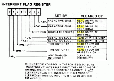
are affected by reads (dummy or otherwise). By design, they attach extra activity to a read. For example, reading the Interrupt Flag Register of a 6522 not only returns the device's interrupt flag status to the CPU; it also clears those flags. Because flag status is erased this is called a "destructive read" -- the 6522 IFR is said to be "read sensitive." It's convenient to have the interrupt flags automatically cleared after a read, but only if you coded the read explicitly -- not when it gets slipped in behind your back!

Other I/O devices -- generally not from the 65xx or 68xx families -- may be read-sensitive in a different way. They require an idle period between accesses. For example, a read followed too closely by another read (or write) might cause the device to become confused. Presumably you've studied the datasheet, and if such a specification exists then your code will be written to provide the necessary delay between accesses. Your plans will be spoiled if a rogue read occurs in the midst of some legitimate accesses.

-- Managing VDA. Managing without VDA. --

The 65816 and 65c816 CPUs do have the necessary pins to command memory-I/O to do nothing. There are various ways these pins (VPA and VDA) can be connected, but the key point is to ensure read-sensitive devices can't be activated when VDA is low. Preventing activation usually means withholding the device's chip-select somehow. Alternatively, non-65xx/68xx I/O devices use read-enable and write-enable inputs called /RD and /WR or something similar, and withholding the signals to those pins is another way to prevent activation. (Withholding /WR is probably unnecessary. AFAIK all dummy cycles are reads except the M of an RMW when in Emulation mode.)

VDA can be very helpful, but attaching the necessary circuitry isn't always an attractive option, and most 65xx CPUs don't feature a VDA pin anyway. The alternative is to ensure that addresses produced during dummy cycles don't coincide with addresses that map to sensitive I/O devices. We can control where I/O devices appear because the address map is a function of our hardware design. And we can control which dummy addresses (aka invalid addresses) appear -- they depend on our coding practices and on the choice of CPU. Here are three problem scenarios and their possible remedies:

Code:
TRB   I-O_Device    ;this device requires an idle period between accesses
Read-Modify-Write instructions such as INC and TRB result in three successive cycles during which the address bus bears the address of the device, and the device must activate at least for the 1st and 3rd of these cycles -- the read and the write. The 2nd cycle is a dummy, during which the CPU internally performs the "modify." During the dummy cycle the CPU's R/W pin will indicate either a read (65c02), a write (6502) or either a read or write, depending whether Emulation mode prevails ('816). If VDA is used then the device won't activate and R/W means nothing. The dummy cycle gives the device a one-cycle pause... which might be long enough to serve as an idle period between the cycle 1 and 3 accesses. If VDA isn't used then the 2nd cycle will be an actual read or write (which is probably not alright, given the activity in 1 and 3). You might be tempted to simply avoid using R-M-W with a device like this! Just remember that even a closely-spaced LDA and STA (ie, not R-M-W) could violate the spec, depending on the value cited.

Code:
STA   Block_Of_I-O_Devices,X   ;the intended device requires an idle period between accesses
This example uses absolute,X address mode, which is one of the indexed address modes which, due to a possible page crossing, can result in a dummy cycle immediately before the intended access. When this kind of dummy cycle appears on 6502 or '816 the address bus will bear either:
  • a partially-processed address which, because carry is 0, needs no further processing and is okay as-is, OR...
  • a partially-processed address which, because carry is 1, is $100 too low and needs its high-byte incremented.
    (I mean carry from the low-bye of the index addition. The carry has not yet propagated into the high byte to produce the page crossing that's required.)

The problem illustrated in the code example happens when there's no page crossing and a dummy cycle is present anyway. (LDA will never do this, but STA can.) The correct address will be present during the dummy cycle and during the intended access which immediately follows -- IOW a double access, which can violate the device's spec requiring an idle period between accesses.

One possible remedy is to use 65c02, which is documented as placing PC on the address bus when indexing is about to produce a page crossing. This prevents device activation because PC says where your instruction bytes are being fetched from, and that'll be an address that maps to memory, not I/O. VDA is another possible remedy.

If VDA can't be used then we could simply avoid using indexed addressing -- but that's wimpy, and costs functionality. :oops: A better solution is to re-code the indexed addressing in a way that guarantees a page crossing! :mrgreen: For example use an address ending in $FF as your base address, with an index that's always >= 1. This will eliminate the double access because the address during the dummy cycle will be $100 below the device. (Specifically, the low-byte of the address during the dummy will be the sum of the low-bytes of the index and the base address. The high-byte will be simply the high-byte of the base address -- no carry included yet.)

Code:
STA   Memory_Array,X      ;a 6522 or other read-sensitive I/O device is located $100 below the intended target in memory
Here's another example that involves indexed addressing and 6502 or '816. In this case a problem results when a page crossing does occur. The partially-formed address during the dummy cycle can touch the I/O device that happens to lie $100 below the intended target. 65c02 is one possible remedy since, as noted, it places PC on the address bus during dummy cycles related to page crossing. VDA is another possible remedy, as it directly prevents device activation during the dummy cycle. Two other solutions exist. We could mentally check ourselves every single time we code some indexed addressing. :roll: But a more palatable and less error-prone solution is to arrange the memory map so the 6522 has at least $100 of unpopulated space above it -- a sort of "no-fly zone"! Leaving the region unpopulated lessens the chance you'll accidentally code an indexed access into what's stored there. :)


I think that covers all the main points. I should mention that dummy cycles can arise from other causes, and VDA protects against them all. But IMO the "other causes" protection is hardly needed since the addresses involved are virtually guaranteed to map to memory, not I/O. (The addresses come from the stack pointer or are addresses pertaining to a MVP or MVN operation.)

Unfortunately our understanding of dummy-cycle behavior relies very heavily on manufacturers' documentation, which may include errors, omit details or lack clarity. For that reason and others, it's possible you'll fall victim to a read-sensitivity problem someday, so it pays to remember the symptoms should they arise. For example the interrupt-flag thing will seemingly cause interrupts (or at least the flag status) to disappear, and that will be an utterly baffling problem to troubleshoot if you've forgotten about the read sensitivity of the 6522's IFR. (ORA, ORB, SR, T1L and T2L are also read-sensitive in some respects but, as with IFR, you'll suffer no consequences unless you're actually using the associated function. And the 6522 is still a very useful chip even without these functions.)
Attachment:
6522 IFR.gif
6522 IFR.gif [ 83.3 KiB | Viewed 2366 times ]


Finally, another reason you might face destructive-read symptoms is a programming trick that replaces a forward BRA such as $80 $02 (ie; skip the following two bytes) with $CD (a CMP absolute opcode, whose intended purpose is merely to absorb the following two bytes as its operand). When the CMP absolute executes it generates a read cycle which may touch an I/O device. The cycle is NOT a dummy, and VDA circuitry won't neutralize it.

-- Jeff

_________________
In 1988 my 65C02 got six new registers and 44 new full-speed instructions!
https://laughtonelectronics.com/Arcana/ ... mmary.html


Top
 Profile  
Reply with quote  
PostPosted: Mon Sep 07, 2015 8:21 am 
Offline

Joined: Mon Jan 07, 2013 2:42 pm
Posts: 576
Location: Just outside Berlin, Germany
Dr Jefyll wrote:
Scot, that description needed a rewrite, which I humbly present below.
Wow. Thank you, exchanged the link, and learned a lot in the process as well. Thank you!


Top
 Profile  
Reply with quote  
Display posts from previous:  Sort by  
Post new topic Reply to topic  [ 25 posts ]  Go to page Previous  1, 2

All times are UTC


Who is online

Users browsing this forum: No registered users and 14 guests


You cannot post new topics in this forum
You cannot reply to topics in this forum
You cannot edit your posts in this forum
You cannot delete your posts in this forum
You cannot post attachments in this forum

Search for:
Jump to: