6502.org Forum  Projects  Code  Documents  Tools  Forum
It is currently Sat May 04, 2024 11:09 pm

All times are UTC


Post new topic Reply to topic  [ 40 posts ]  Go to page 1, 2, 3  Next
Author Message
 Post subject: The J64C (version 0)
PostPosted: Mon Jul 12, 2021 11:28 pm 
Offline

Joined: Sun Jul 11, 2021 9:12 am
Posts: 137
Hi Guys!

Thanks for welcoming me to your community, back over in my question thread. The responses have been truly amazing and I am quickly feeling that this is a great little community!

You'll find that my project is pretty bare bones at the moment as I am a complete newbie to the W65C02 CPU. But growing up as a kid with the Commodore 64 in the 80's has made me very fond of the 6502/10.

My lofty goals are to make a full computer with VGA output. Before you say "Oh god, here we go :? " don't stress, I'm in no rush and am in it for the long haul. And besides, I have already built the functional VGA board. :lol: I started this project in what people would consider to be reverse order.

Attachment:
a3.jpg
a3.jpg [ 137.31 KiB | Viewed 1140 times ]


Now we have that out of the way. I have started the CPU side of things by being very minimalistic, mainly because I am new to this side of things and will be very much experimenting with timings etc, until I get a firm understanding of what keeps the W65C02 happy. If it's happy, I'm happy! :D

This is the bare bones circuit that I have started with, that I will expand upon.

Attachment:
a1.png
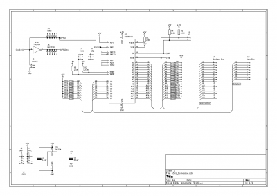
a1.png [ 80.82 KiB | Viewed 1140 times ]


The reason for the inverter there, is related to the 'BE' usage question, where I wanted to be able to invert the clock and put the CPU in to high-Z on the lower cycle. As I have found, it's not as simple as just doing that (did have some success though yesterday) so the inverter can be ignored.

I created a stripboard, with heaps of header pins so I can connect other boards (like RAM etc.). I am pretty OCD with my stripboards. I tend to put the effort into going straight to stripboards as I am yet to find a breadboard that works reliably, they always seem to be a constant fight to get decent connections.

Attachment:
a0.jpg
a0.jpg [ 71.3 KiB | Viewed 1140 times ]


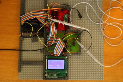
I have also made my own logic analyser, which I am monitoring the data and address bus with, and also acts as the clock to the 6502. Here's a pic of when I put it together after receiving the boards back from PCBWay after designing them. In the pic, I was just testing all of the I/O's to make sure it worked as planned, which it did! 8)

Attachment:
a4.jpg
a4.jpg [ 65.87 KiB | Viewed 1140 times ]


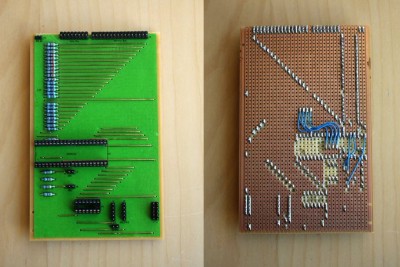
The CPU gets it's ROM/RAM from another board I made which I call "FlashRAM 128". I needed a nice and easy way to be able to get programs to run on the 6502. It has a Raspberry Pi Pico, which pre-populates the RAM with whatever I want on it. It also holds the CPU in high-z, then resets it.

Here it is pre-loading the RAM on the aforementioned VGA card during early testing. The FlashRAM is the red board the VGA is two blue boards hooked together.

Attachment:
a5.jpg
a5.jpg [ 119.17 KiB | Viewed 1140 times ]


The 'FlashRAM' can either house a 128KB ram chip or can talk to external directly RAM.

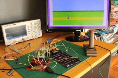
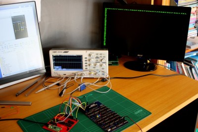
So here it is in its present form, all interconnected. I am dumping the program directly on to the VGA RAM board (holding the rest of the VGA boards circuit in high-z, so the CPU has exclusive use right now) and it is all happy running a simple program at around 2 Hz.

Attachment:
a6.jpg
a6.jpg [ 252.59 KiB | Viewed 1140 times ]


Attachment:
a7.jpg
a7.jpg [ 10.43 KiB | Viewed 1140 times ]


I know I'm not going to win any speed records with the current setup, it's purely to gain confidence and understanding of how the 6502 ticks.

So there you go! A fairly long winded first post. But hopefully this will give a bit of an insight as to where I'm coming from. Not afraid to get my hands dirty and not afraid to put my hand up when I don't know something. Hehe!

All feedback and questions are welcome. :D


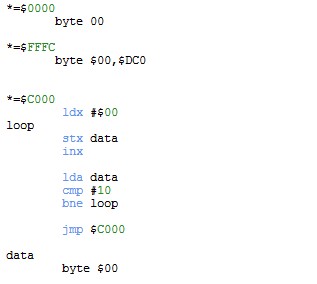
(Typo in the reset vector - should read $C0 not $DC0. I mustn't have hit save last night when I corrected that)


Top
 Profile  
Reply with quote  
 Post subject: Re: The J64C (version 0)
PostPosted: Tue Jul 13, 2021 5:40 am 
Offline
User avatar

Joined: Thu May 28, 2009 9:46 pm
Posts: 8173
Location: Midwestern USA
Minor note: A0-A15 and RWB are outputs, not inputs. Pullup resistors on those lines are unnecessary and while their presence won't hurt anything (assuming they are of sufficient resistance), I recommend you remove them, as they constitute parasitic loading when one of those outputs is at logic 0. The 65C02 drives its outputs from rail to rail and needs no help in putting out a solid CMOS logic 1.

Regarding clock generation, I'll reiterate what I said in your other topic. The clock rise/fall time must be very fast. WDC specifies 5ns or faster. You can cheat to some extent, but if you stray too far from their specs there's no telling what will happen. Exactly what are you using as a clock source?

Lastly, the 74LS04 is unsuitable for your application. That should be a CMOS device, e.g., a 74HC04.

_________________
x86?  We ain't got no x86.  We don't NEED no stinking x86!


Top
 Profile  
Reply with quote  
 Post subject: Re: The J64C (version 0)
PostPosted: Tue Jul 13, 2021 5:58 am 
Offline

Joined: Sun Jul 11, 2021 9:12 am
Posts: 137
Hi BDD, thanks for the tips.

I mentioned in the thread that the clock source is presently a Raspberry Pi Pico, which I am also using to monitor and report back what is on the data and address lines. I measured the rise and fall times and they are both around 4.5ns.

With the 74LS04, I also mentioned that it has been removed from the circuit entirely and can be ignored from the schematic.

I certainly wasn't aware of not requiring pull-ups on the address lines. I'll look at removing those. FWIW - My diagram says 2.0K on all of the resistors. But I opted with 3.3K in the end. I think it was Garth's primer that made me go for higher values in the end. I didn't want to inadvertently load things down too much.


Top
 Profile  
Reply with quote  
 Post subject: Re: The J64C (version 0)
PostPosted: Tue Jul 13, 2021 6:24 am 
Offline
User avatar

Joined: Thu May 28, 2009 9:46 pm
Posts: 8173
Location: Midwestern USA
J64C wrote:
I certainly wasn't aware of not requiring pull-ups on the address lines. I'll look at removing those. FWIW - My diagram says 2.0K on all of the resistors. But I opted with 3.3K in the end. I think it was Garth's primer that made me go for higher values in the end. I didn't want to inadvertently load things down too much.

Anything that is exclusively an output on the 65C02 needs no pullup and as I earlier said, adding one merely adds to the current flow when the output is at logic 0. All control inputs must be pulled up to Vcc or positively driven in both directions, with the lone exception of RDY. RDY should never be directly driven by another device's output—series resistance, or a pullup resistor in concert with a Schottky diode should be used to avoid contention should RDY be driven low by the MPU while something is trying to drive it high.

_________________
x86?  We ain't got no x86.  We don't NEED no stinking x86!


Top
 Profile  
Reply with quote  
 Post subject: Re: The J64C (version 0)
PostPosted: Tue Jul 13, 2021 6:39 am 
Offline

Joined: Sun Jul 11, 2021 9:12 am
Posts: 137
Awesome! Many thanks for the clarification. Even makes the circuit much simpler as a result.


Top
 Profile  
Reply with quote  
 Post subject: Re: The J64C (version 0)
PostPosted: Tue Jul 13, 2021 10:47 pm 
Offline

Joined: Sun Jul 11, 2021 9:12 am
Posts: 137
I've updated the core of the project, removing the unused IC and capacitor, also removed the bus pull-ups as per BDD's suggestion. Changed the values of the resistors to 3.3K to reflect what I have in the prototype board. I'll leave the data line pull-ups in the circuit diagram for now and look at the possibility of removing them as the project matures.
Attachment:
core.png
core.png [ 64.09 KiB | Viewed 1063 times ]


Top
 Profile  
Reply with quote  
 Post subject: Re: The J64C (version 0)
PostPosted: Wed Jul 14, 2021 1:38 am 
Offline

Joined: Sun Jul 11, 2021 9:12 am
Posts: 137
BigDumbDinosaur wrote:
Lastly, the 74LS04 is unsuitable for your application. That should be a CMOS device, e.g., a 74HC04.[/color]


Is this because of the logic levels?


Top
 Profile  
Reply with quote  
 Post subject: Re: The J64C (version 0)
PostPosted: Wed Jul 14, 2021 7:28 am 
Offline
User avatar

Joined: Thu May 28, 2009 9:46 pm
Posts: 8173
Location: Midwestern USA
J64C wrote:
BigDumbDinosaur wrote:
Lastly, the 74LS04 is unsuitable for your application. That should be a CMOS device, e.g., a 74HC04.

Is this because of the logic levels?

Correct.

74LS logic has a guaranteed logic 1 output of 2.4 volts when operating on 5 volts. The output may be higher if loading is very light (3.4 volts maximum in theory), but that is not guaranteed and cannot be relied upon. A CMOS device (that is, 74xC) expects an input level of at least 3.5 volts to recognize a logic 1.

In cases where a CMOS device's inputs must interface with a 74LS device's outputs the CMOS device should be 74xCT, which has TTL-compatible inputs.

Aside from logic level differences, 74LS devices have relatively weak outputs, which limits how much loading they can tolerate. CMOS devices generally drive rail-to-rail and better handle loading.

_________________
x86?  We ain't got no x86.  We don't NEED no stinking x86!


Top
 Profile  
Reply with quote  
 Post subject: Re: The J64C (version 0)
PostPosted: Wed Jul 14, 2021 7:44 am 
Offline

Joined: Sun Jul 11, 2021 9:12 am
Posts: 137
Thanks for the detailed reply.

So going by the manual (and assuming 5v as he source), an acceptable logic high is 3.5v to 5.3v and low is -0.3v to 1.5v.
Attachment:
question.png
question.png [ 29.88 KiB | Viewed 1031 times ]

That gives a pretty nice leeway compared to TTL. I can certainly see why TTL is not a very good choice when interfacing it directly to the W65C02.


Top
 Profile  
Reply with quote  
 Post subject: Re: The J64C (version 0)
PostPosted: Wed Jul 14, 2021 8:19 am 
Offline
User avatar

Joined: Fri Aug 30, 2002 1:09 am
Posts: 8432
Location: Southern California
J64C wrote:
So going by the manual (and assuming 5v as he source), an acceptable logic high is 3.5v to 5.3v and low is -0.3v to 1.5v.

I suspect that the space between 1.5 and 3.5V may get interpreted correctly in many cases, ie, that above and below 2.5V is interpreted as 1 or 0 respectively, but slowing the response time such that it no longer meets the timing specs. The only way to know for sure it to test it ourselves, since the data sheet doesn't say. Otherwise, yeah, just follow the spec to stay out of trouble. :) The reality is usually better than the specs; but if we start depending on it being better, we're kind of on our own. It may work fine; it's just not guaranteed.

Going outside the rails by .3V is approximately where the static-protection diodes start conducting. Although they can give some protection against static, they are indeed tiny (so as to minimize input capacitance), and would probably be blown out (and turned into a short) if the conduction time and duty cycle isn't really low. Some overshoot following a rising or falling edge, resulting from less-than-perfect construction, probably won't damage the part. I've never damaged anything from overshoot.

I definitely advocate for 74HC (or HCT) over 74LS. 74AC (or ACT) and certain other 74___ families will be more suitable when you start turning up the speed, but may require better construction to avoid AC-performance problems. Just stay away from CD4000 series, as it is painfully slow at 5V. Save that for when you need logic functions at 12V.

It's always good to ask; but sometimes we just have to resort to that nebulous term, "good engineering practice," which means we take it everything we know, and recognize that there are factors we don't know or can't model, and come up with our best guess, and go for it.

_________________
http://WilsonMinesCo.com/ lots of 6502 resources
The "second front page" is http://wilsonminesco.com/links.html .
What's an additional VIA among friends, anyhow?


Top
 Profile  
Reply with quote  
 Post subject: Re: The J64C (version 0)
PostPosted: Wed Jul 14, 2021 9:34 am 
Offline

Joined: Sun Jul 11, 2021 9:12 am
Posts: 137
GARTHWILSON wrote:
It's always good to ask; but sometimes we just have to resort to that nebulous term, "good engineering practice," which means we take it everything we know, and recognize that there are factors we don't know or can't model, and come up with our best guess, and go for it.


It's funny that you mention that, because I been doing some tests of my own this evening (I'm very much a try things in practise kind of person) and found some interesting results.

I was looking at making a better clock circuit by feeding a ~25 MHz oscillator can in to a 74HC4040, so I can use that as a clock divider. Maybe even cascading two of them so I can keep halving the clock all the way down to around 1Hz at the extreme low end.

Running all of this initially from a bread board (which I'm not a huge fan of at the best of times) gave me this lovely wave form, at one of the 74HC4040's outputs.

Attachment:
00.png
00.png [ 12.7 KiB | Viewed 1016 times ]


Needless to say I was mortified by the result.


So I thought I'd do some experimenting. Starting by placing the components close together using standard hook up wires.

The result was much better.

Attachment:
aaa.jpg
aaa.jpg [ 200.4 KiB | Viewed 1016 times ]


Which then got me thinking. What if I take Garths advice and take the shortest path?

Attachment:
bbb.jpg
bbb.jpg [ 213.23 KiB | Viewed 1016 times ]


Even better! Now let's see what happens if we add icing to the cake by adding a 0.1uF capacitor (shortest path again) across the supply pins?

Attachment:
ccc.jpg
ccc.jpg [ 207.3 KiB | Viewed 1016 times ]


Even better again!

So it just goes to show you, placement is absolutely key! Not that I ever doubted you. But it's a very interesting exercise to see the different before your own eyes!


Top
 Profile  
Reply with quote  
 Post subject: Re: The J64C (version 0)
PostPosted: Wed Jul 14, 2021 9:40 am 
Offline
User avatar

Joined: Fri Aug 30, 2002 1:09 am
Posts: 8432
Location: Southern California
Next would be to complete the triangles of the blue and orange wires. :)

_________________
http://WilsonMinesCo.com/ lots of 6502 resources
The "second front page" is http://wilsonminesco.com/links.html .
What's an additional VIA among friends, anyhow?


Top
 Profile  
Reply with quote  
 Post subject: Re: The J64C (version 0)
PostPosted: Wed Jul 14, 2021 10:10 am 
Offline

Joined: Sun Jul 11, 2021 9:12 am
Posts: 137
Very true! Or I could even ditch the breadboard power rails and go direct. I might try that out in the morning, out of interest. All packed up for the night here (in Australia).


Top
 Profile  
Reply with quote  
 Post subject: Re: The J64C (version 0)
PostPosted: Thu Jul 15, 2021 1:29 am 
Offline

Joined: Sun Jul 11, 2021 9:12 am
Posts: 137
Abstract side question.

If a HC CMOS (assuming 5V power source) sees a logic low as 0V to 2.1V and a logic high as 2.4V to 5V, that would make the rise time here 0.32nS wouldn't it?
Attachment:
quiz.png
quiz.png [ 11.37 KiB | Viewed 965 times ]

You'd calculate the time between the 'valid' states for the device type wouldn't you? Obviously taking consideration of the type of the next device in the chains capabilities.


Top
 Profile  
Reply with quote  
 Post subject: Re: The J64C (version 0)
PostPosted: Thu Jul 15, 2021 1:38 am 
Offline
User avatar

Joined: Fri Aug 30, 2002 1:09 am
Posts: 8432
Location: Southern California
It looks more like about 3ns. Rise time is generally considered to be from 10% to 90%.

_________________
http://WilsonMinesCo.com/ lots of 6502 resources
The "second front page" is http://wilsonminesco.com/links.html .
What's an additional VIA among friends, anyhow?


Top
 Profile  
Reply with quote  
Display posts from previous:  Sort by  
Post new topic Reply to topic  [ 40 posts ]  Go to page 1, 2, 3  Next

All times are UTC


Who is online

Users browsing this forum: No registered users and 12 guests


You cannot post new topics in this forum
You cannot reply to topics in this forum
You cannot edit your posts in this forum
You cannot delete your posts in this forum
You cannot post attachments in this forum

Search for:
Jump to: